Electroluminescence from h-BN by using
Al
2O
3/h-BN multiple heterostructure
S
EUNGH
EEL
EE,
1H
OKYEONGJ
EONG,
1D
ONGY
EONGK
IM,
1S
EUNG-Y
OUNGS
EO,
1,2C
HEOLHEEH
AN,
1,2O
DONGOF
RANCISN
GOMEO
KELLO,
1J
EN-I
UL
O,
3Y
U-C
HAINP
ENG,
3C
HAN-H
YOUNGO
H,
4G
YEONGW
ONL
EE,
4J
ONG-I
NS
HIM,
4B
ING-M
INGC
HENG,
3K
YUNGS
ONG,
5S
I-Y
ONGC
HOI,
1M
OON-H
OJ
O,
1,2ANDJ
ONGK
YUK
IM1,*1Department of Materials Science and Engineering, Pohang University of Science and Technology, Pohang 37673, South Korea
2Center for Artificial Low Dimensional Electronic Systems, Institute for Basic Science (IBS), Pohang 37673, South Korea
3National Synchrotron Radiation Research Center, Hsinchu 30076, Taiwan
4Department of Electronics and Communication Engineering, Hanyang University ERICA, Ansan 15588, South Korea
5Materials Modeling and Characterization Department, Korea Institute of Materials Science (KIMS), Changwon, 51508, South Korea
Abstract: Two-dimensional (2-D) hexagonal boron nitride (h-BN) has attracted considerable
attention for deep ultraviolet optoelectronics and visible single photon sources, however, realization of an electrically-driven light emitter remains challenging due to its wide bandgap nature. Here, we report electrically-driven visible light emission with a red-shift under increasing electric field from a few layer h-BN by employing a five-period Al2O3/h-BN
multiple heterostructure and a graphene top electrode. Investigation of electrical properties reveals that the Al2O3 layers act as potential barriers confining injected carriers within the
h-BN wells, while suppressing the electrostatic breakdown by trap-assisted tunneling, to increase the probability of radiative recombination. The result highlights a promising potential of such multiple heterostructure as a practical and efficient platform for electrically-driven light emitters based on wide bandgap two-dimensional materials.
© 2019 Optical Society of America under the terms of the OSA Open Access Publishing Agreement 1. Introduction
Two-dimensional (2D) materials including graphene, hexagonal boron nitride (h-BN) and transition metal dichalcogenides (TMDs) are crystallized in atomically thin-layered structures held together by strong in-plane covalent bonds and weak out-of-plane van der Waals bonds. The 2D material systems have been under intensive investigation for applications in many fields such as electronics [1], optoelectronics [2,3], photocatalytic [4] and sensing applications [5] owing to their unique and fascinating physical properties [6]. Among the family of 2D materials, h-BN, consisting of sp2-bonded boron and nitrogen atoms, has been proposed as a
promising luminescent material for deep ultraviolet (DUV) optoelectronic devices since it exhibits the wide bandgap of approximately 6 eV [7–10].
The emission of photons from h-BN has been studied by utilizing cathodoluminescence (CL) and photoluminescence (PL) spectroscopies. Watanabe et al. [7,11] reported a sharp luminescence peak at 5.77 eV (215 nm) attributed to the direct exciton recombination in the h-BN single crystal and luminescence peaks at 5.63 (220) and 5.46 eV (227 nm) appear as a result of the recombination of trapped excitons at structural defects. On the other hand, Cassabois et
al. [10] reported that phonon-assisted optical transitions are responsible for the observed PL
emission peaks from h-BN having indirect bandgap of 5.995 eV. A quantitative study of the
#365214
CL in h-BN revealed the internal quantum yield of 15%, comparable to that of direct bandgap ZnO, enabled by the strong coupling of excitons with phonons in h-BN [12]. In addition, there have been several studies on the deep-level transitions in ultraviolet (UV) range as well as near-band-edge emission. According to Jiang et al. [13,14], the broad peaks covering from 3.7 to 4.1 eV are ascribed to the donor-acceptor pair transition involving nitrogen vacancy donor states and deep level acceptor states resulting from substitutional carbon impurities on nitrogen sites. Based on the investigations of the luminescence properties, there have been efforts to develop light emitters by utilizing h-BN as an active layer. h-BN has been demonstrated as a fascinating room temperature PL single photon source in visible range (500−700 nm) [15–19], in which the nature of the single photon emission center is unclear though it is likely associated with the deep-level atomic defects such as the nitrogen-anti-site defect (NBVN) [20]. On the
other hand, h-BN-based UV CL devices equipped with field-emission cold cathodes have been developed as an alternative to conventional lamps [21,22]. However, the high operating voltage (120-900 V) for field emission [23] and low compatibility with conventional micro-fabrication limit their integrated photonic and optoelectronic applications.
Electrically-driven electroluminescence (EL) light sources would be much more advantageous than PL- and CL-based sources in terms of efficiency, integrability and scalability [24]. While h-BN layers have been typically used as passive dielectric materials for TMD-based (opto)electronic devices, it is challenging to realize an electrically-driven light emitter with h-BN active layer due to its wide bandgap nature. The difficulties in doping, and hence, in the formation of a stable p-n junction and ohmic contacts [25] limit the injection of electrons and holes. In addition, the low mobility-life time products for electrons and holes in h-BN (~5.8 × 10⁻⁸ and ~6.1 × 10⁻⁹ cm2 V−1, respectively [26]) decline the transport of charges
as well as the formation of excitons, further limiting EL from h-BN.
In this study, we present electrically-driven visible light emission from the EL device consisting of a 5-period Al2O3/h-BN multiple heterostructure. While similar PL spectra in DUV
and visible wavelength ranges were observed both from the h-BN-only structure and the Al2O3/h-BN heterostructure, visible EL emission with a red-shift under increasing electric field
was observed only from the heterostructure device. Based on the electrical properties of the devices, it is believed that the 3 nm-thick Al2O3 layers act as potential barriers for an effective
confinement of injected carriers within the 9 nm-thick h-BN wells, enhancing the probability of radiative recombination while avoiding the electrostatic breakdown through defect states in the h-BN active layer.
2. Experimental details
2.1 Device fabrication
The 5-period Al2O3/h-BN multiple heterostructure was fabricated on a patterned Pt bottom
electrode by repeating the deposition of a 3-nm-thick Al2O3 at 300 °C by atomic layer
deposition (ALD) followed by the transfer of a ~9 nm-thick multilayer h-BN, grown by chemical vapor deposition (CVD) method on the copper foil (from Graphene Supermarket), using polymethyl methacrylate (PMMA) supported wet transfer technique. After the deposition of the 6th Al
2O3, a graphene (CVD-grown monolayer graphene from Graphene Square Inc.) top
electrode was transferred onto the stack by using the wet transfer method as well, followed by Ti/Au (5/100 nm) deposition for electrical contacts to the top graphene electrodes.
2.2 Microscopic, electrical and optical characterizations
A JEM-ARM2100F scanning transmission electron microscope (STEM) operated at 60 kV with up to 5th order aberration-correction was employed to investigate the cross-sectional image
of the vertical devices. The samples were prepared by dual beam focused ion beam (FIB) (FEI, Helios Nano-Lab 600) milling with final milling done at 0.5 kV to minimize sample damage. Core level X-ray photoelectron spectroscopy (XPS) measurements of ALD-deposited Al2O3
were performed using a Perkin-Elmer PHI 5400 ESCA spectrometer. Optical characterization including absorbance and PL in DUV range were carried out by using the synchrotron radiation at the BL03A high flux VUV beam line at National Synchrotron Radiation Research Center, Taiwan at 10 K. In this work, a monochromator (iHR 320, HORIBA) equipped with a diffraction grating of 1800 lines mm−1 and slit size of 1
×
1 mm2 and a photomultiplier tube(PMT, Hamamatsu R943-02) were used and the entrance and exit slit widths were set at 300 and 5,000 μm, respectively. To measure PL in visible range, the samples were excited with a continuous wave 532 nm laser, focused through a × 10 objective and attenuated by an ND filter 9. The PL was collected by a monochromater (Acton SP2300) equipped with a charge coupled detector (CCD, PIXIS 100). For EL and electrical measurements, the devices were mounted on identical stage to visible PL setup. Electrical injection was performed using an Agilent B2902A source meter, and EL signals were collected by averaging five acquisitions with integration time of 5 seconds using Acton SP2300 monochromater equipped with PIXIS 100 CCD.
3. Results and discussion
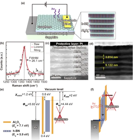
3.1 Fabrication of the Al2O3/h-BN multiple heterostructure
The EL device based on a 5-period Al2O3/h-BN multiple heterostructure was fabricated on a
platinum (Pt) bottom electrode on a sapphire substrate by repeating the deposition of a 3 nm-thick Al2O3 by ALD followed by transferring a 9 nm-thick multilayer h-BN grown by CVD.
After the deposition of the 6th Al
2O3, a CVD-grown graphene layer was transferred on top of
the multiple hetetrostructure as a semitransparent top electrode, as schematically shown in Fig. 1(a). For comparison, h-BN-only and Al2O3-only structures in which the thicknesses of h-BN
and Al2O3 are equal to the total thickness of the h-BN layer and the Al2O3 layer in the multiple
heterostructure, respectively, were fabricated. Figure 1(b) shows the Raman spectrum of the multilayer h-BN with the peak at ~1369.5 cm−1 originating from the E2g mode of B-N bond
in-plane vibration. The full-width-at-half-maximum of the peak is 26.1 cm−1, comparable to previously reported values for the CVD-grown multilayer h-BN [27,28]. The cross-sectional bright field (BF) and high-angle annular dark field (HAADF) STEM images clearly show a well-defined 5-period Al2O3/h-BN heterostructure as shown in Fig. 1(c) and 1(d), respectively.
Since the contrast is roughly proportional to the square of the atomic number, the dark contrast in the HAADF-STEM image corresponds to the h-BN layers while the bright contrast region is the Al2O3 layers. The h-BN layer with (0002) lattice spacing of ~0.33 nm is observed in the
magnified STEM image of the part of multilayer h-BN.
Figure 1(e) shows the ideal energy-band diagrams before making contact between the Pt bottom electrode, the single Al2O3/h-BN/Al2O3 heterostructure, and the graphene top electrode,
constructed by using reported values of electron affinity (2 and 1.2 for h-BN [29] and Al2O3
[30]) and dielectric constant (3.12 and 9 for h-BN [31] and Al2O3 [32]) and experimental values
of optical band gap, 5.9 eV for the h-BN layer and 7.1 eV for the Al2O3 barrier layer estimated
by the Tauc’s plots. Stacking Al2O3 and h-BN layers results in the formation of the h-BN wells
having the barrier heights of 0.8 and 0.4 eV for electron and hole, respectively, with the Al2O3
potential barriers. Under a sufficient forward bias (Fig. 1(f)), the quasi-Fermi level of the graphene layer shifts above defects-related sub-band states or the conduction band edge of the h-BN layer, thus, the injection of electrons and holes into available energy states in the h-BN active layer through the thin Al2O3 barriers via tunneling can occur. The injected carriers can
be effectively confined within the h-BN wells enclosed by the Al2O3 potential barriers,
Fig. 1. Schematic illustration, structural characteristics and energy band diagrams of Al2O3
/h-BN/Al2O3 heterostructure based light emitting device. (a) Schematic illustration of an
electrically-driven EL device consisting of a 5-period Al2O3/h-BN multiple heterostructure and
a Pt-bottom and a graphene-top electrodes. (b) Raman spectrum of the multilayer CVD-grown h-BN with FWHM of 26.1 cm−1. (c) A cross-sectional BF-STEM and (d) the corresponding HAADF-STEM image of the 5-period Al2O3/h-BN multiple heterostructure on a sapphire
substrate. The ideal energy band diagrams (e) before making contacts between a Pt bottom electrode, Al2O3, h-BN, and a graphene top electrode and (f) after making
Pt/Al2O3/hBN/Al2O3/Gr heterostructure under a high forward bias.
3.2 Photoluminescence from the Al2O3/h-BN multiple heterostructure
Figure 2 shows PL spectra of the h-BN-only structure and the Al2O3/h-BN multiple
heterostructure with same total h-BN thickness of ~45 nm. Both samples exhibit two near-band-edge emission lines at around 5.420 and 5.571 eV under synchrotron radiation excitation with the photon energy of 7.09 eV (175 nm) at 10 K as shown in Fig. 2(a). Two emission peaks coincide with the donor-acceptor-pair transition and its one E2g phonon replica, respectively
[33]. It is noticeable that the PL intensity from the Al2O3/h-BN heterostructure is higher than
that from the h-BN-only sample even though the h-BN layers in the heterostructure likely absorbs less excitation photons due to the reflection at multiple interfaces consisting of Al2O3
and h-BN with refractive indices of 1.9 [34] and 1.7 [35], respectively. It can be attributed to the spatial confinement of photo-generated excitons in the h-BN active layers of the
heterostructure that prevents a long-distance diffusion to non-radiative recombination centers and consequentially enhances the probability of radiative recombination [36,37]. Figure 2(b) shows PL spectra in visible wavelength range under laser excitation with the photon energy of 2.33 eV (532 nm) at 77 K. Broad features covering relatively large spectral range appear from both samples. Note that no luminescence was observed from the Al2O3-only sample, indicating
that the possibility of the emission from defect states in the Al2O3 layer can be excluded. (The
abrupt reduction of the intensity around 2.30 eV originates from the 2.33 eV (532 nm) laser notch filter.) According to Koperski et al. [19], the origin of the broad band emission in visible wavelength region is likely related to the ensembles of optical transitions between discrete electronic states located deep in the bandgap derived from structural defects in h-BN. Slightly different shape of the PL spectra of two samples can be attributed to inhomogeneous distribution of emitting defects and unintentional curvatures [38] formed by wrinkles during wet-transfer within ~20 μm-diameter laser excited region.
Fig. 2. Photoluminescence spectra. Comparison of the PL spectra of the h-BN-only and the Al2O3/h-BN multiple heterostructure samples: (a) PL spectra in DUV wavelength range under
175 nm excitation source at 10K and (b) normalized PL spectra in visible wavelength range under 532 nm excitation source at 77 K. Note that total thickness of h-BN in the Al2O3/h-BN
multiple heterostructure is identical to that in the h-BN-only sample.
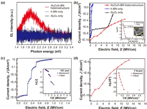
3.3 Electroluminescence and electrical properties of the Al2O3/h-BN multiple heterostructure
Figure 3(a) shows the EL emission from the heterostructure, the h-BN-only, and the Al2O3
-only samples at maximum measured current densities of 2 × 10⁻⁴, 8, and 5.7 × 10⁻³ A cm−2, respectively, according to the current density-electric field (J-E) curves shown in Fig. 3(b) under 77 K. The 5-period Al2O3/h-BN multiple heterostructure shows a broad spectral feature
similar to the PL spectra with maximum intensity at ~1.9 eV, while no luminescence was observed from the devices composed of 45 nm-thick h-BN-only and 18 nm-thick Al2O3-only
structures in spite of higher current density than that of the heterostructure. As discussed with the PL spectra in visible wavelength range, the broad EL emission can be attributed to the defect-mediated emission from the h-BN wells of the Al2O3/h-BN multiple heterostructure.
The Al2O3/h-BN multiple heterostructure device shows the onset electric field of ~9.5 MV
cm−1 while the h-BN-only device shows abruptly increased current density below 1 MV cm−1. The current density for the h-BN-only structure (Fig. 3(c)) is much higher than that for the heterostructure (Fig. 3(d)), as well as shows abrupt multiple jumps at low electrical fields, which is attributed to layer-by-layer breakdown by tunneling [39–41] through defects in the h-BN layer. The logarithm scale J-E curves shown in Fig. 3(c) and 3(d) are further investigated to figure out the carrier transport mechanism of each sample. It has been reported that the transport of charge carriers in both multilayer h-BN and high-quality Al2O3 dominantly follows
triangular barrier in the presence of a high electric field. However, each step in the J-E curve for the h-BN-only structure fits well with trap-assisted tunneling (TAT) model,
3/ 2
( t / ),
J=Aexp − ΦB E rather than F-N tunneling, 2 3/ 2
( / B) ( B / )
J= CE Φ exp− ΦD E , where A,
B, C and D are constants, E is the applied electric field, Φt is the trap energy level, and ΦB is the tunneling barrier height. The values of Φt are ranging from 0.11 to 0.18 eV estimated from slopes of the TAT plot, much lower than the reported tunneling barrier height of 1.5 eV for few layer of defect-free h-BN sandwiched by graphene electrodes [44] due to the higher density of defects such as nitrogen vacancies [45] in CVD-grown multilayer h-BN than in exfoliated h-BN from a single crystal. On the other hands, the J-E curves of both the heterostructure and the Al2O3-only structure under high external electric field fit well with the
F-N tunneling model as shown in Fig. 3(d) and the inset of Fig. 3(b). The effective ΦB of the heterostructure is estimated to be 0.89 eV, which is higher than that for the h-BN-only structure, with assumed effective mass of 0.5m0 [46] (m0 is the free electron mass). Based on the distinct
difference in the J-E curve and the EL emission between the h-BN-only and the Al2O3/h-BN
heterostructure, we believe that the Al2O3 layers play an important role as potential barriers that
suppress the carrier leakage by trap-assisted tunneling process in the h-BN layers that resulted in the abrupt multiple jumps in current density by layer-by-layer breakdown at low electric fields for the h-BN-only device. In addition, the Al2O3 layers form potential barriers with the
h-BN wells in the heterostructure, leading to an enhanced confinement of injected carriers, increasing the probability of radiative recombination of the carriers.
Fig. 3. Electroluminescence and electrical characterization. (a) EL spectra from the Al2O3/h-BN
multiple heterostructure, the h-BN-only, and the Al2O3-only samples measured at maximum
current densities of 2 × 10⁻⁴, 8, and 5.7 × 10⁻³ A cm−2, respectively. (b) J-E curves of the Al2O3
-only, the h-BN-only and the Al2O3/h-BN multiple heterostructure based device in logarithmic
scale. The inset shows Fowler-Nordheim (F-N) plots of the Al2O3-only sample at high electric
field region. The extracted tunneling barrier height of 3.15 eV is close the difference between the CB edge and graphene Fermi-level. A cross-sectional TEM image shows the 18 nm-thick Al2O3 deposited by ALD on Pt. Scale bar is 2 nm. J-E curves of (c) the h-BN-only and (d) the
heterostructure based devices in logarithmic scale. Each inset shows linear data fitting for trap assisted tunneling (TAT) and F-N tunneling, respectively.
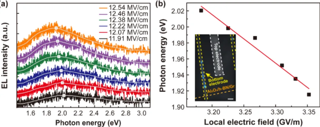
Figure 4(a) shows the change of EL spectra with increasing electric field to the Al2O3/h-BN
heterostructure device at 77 K. The intensity of the EL spectra increases, accompanying a red-shift of the peak energy from 2.02 eV to 1.92 eV with increasing the electric field from 11.91 to 12.54 MV cm−1. This indicates that the possibility of a black-body radiation by Joule’s heating and a hot carrier mechanism, which result in a blue-shift of emission peak with increasing bias, can be excluded to explain the electrically-driven emission in visible range from the Al2O3/h-BN multiple heterostructure.
The red-shift in the EL spectra with increasing electrical field could be elucidated by Stark effect. According to Chakraborty et al. [47], Stark effect of individual defects has been demonstrated by applying a vertical electric field to the defects in van der Waals heterostructures consisting of atomically thin WSe2, resulting in an efficient spectral tunability
up to 21 meV. Stark tuning of single-photon emission from atomic defects in h-BN as large as 5.4 nm per GV m−1 has been observed as well [48] owing to dipole moment of various defects in h-BN ranging from −0.9 to 0.9 D (1 D = 3.33 × 10⁻³⁰ Cm) under external electric field.
Dipole moment of 29.31 D, much higher than the reported values, was extracted from the linear fit of the photon energy shift versus local electric field curve of the Al2O3/h-BN multiple
heterostructure, as shown in Fig. 4(b). This indicates that, together with Stark effect, other additional effects including activation of new atomic defect states by electrical stress [49] may be responsible for the red-shift in the EL spectra. The inset of Fig. 4(b) shows the image of the Al2O3/h-BN heterostructure device overlaid with discrete EL emission spots on the bottom
electrode region observed by a charge-coupled device. Multiple emission spots vary in location under different applied electric field, which can be elucidated by generation and annihilation of defect-related recombination centers during external electrical stress. Moreover, bandgap shrinkage induced by heat generation [50], which is also observed in other solid-state emitters at the high injection current level [51,52] can be one of the possible reasons considering the large bandgap shrinkage parameter of h-BN due to strong electron-phonon interaction [33].
Fig. 4. (a) EL spectra showing a red-shift under increasing applied field from 11.91 to 12.54 MV cm−1. Smoothened white solid lines and square dots are drawn to guide the eyes for the peak position. (b) Plot of Stark shift versus local electric field for the spectra shown in (a). The inset image shows the device overlaid with the colored EL emission spots observed by a CCD. Scale bar is 40 μm.
4. Conclusion
We demonstrated an electrically-driven visible light emitter based on a 5-period Al2O3/h-BN
multiple heterostructure. PL spectra with similar peak positions in DUV and visible wavelength ranges were observed both from the h-BN-only structure and the Al2O3/h-BN heterostructure,
while the intensity of the DUV PL from the heterostructure is larger than that from the h-BN only structure. On the other hand, electrically-driven photon emission, EL, was observed only from the heterostructure device. Based on the investigation of the electrical properties of the
devices, the 3 nm-thick Al2O3 layers play an important role as potential barriers for an effective
confinement of injected carriers within the 9 nm-thick h-BN wells, enhancing the probability of radiative recombination as well as suppressing the trap-assisted tunneling process, and hence, the electrostatic breakdown in the h-BN layers. The broad visible EL spectrum with peak intensity at ~1.9 eV is ascribed to the ensemble of optical transitions via structural defects in the h-BN layers. The red-shift in the EL spectra by 0.102 eV under increased bias from 11.92 to 12.54 MV cm−1 was observed, which is possibly owing to the combination of multiple effects including Stark effect, change of active defect states by electrical stress, and bandgap shrinkage at high current injection. We believe that further intensive works utilizing a high quality h-BN with well-controlled defects and precisely manipulated potential barrier will allow to realize an electrically-driven light emitter with intended EL spectra such as excitonic emission in DUV range and wavelength-controlled single photon emission from h-BN active layers.
Funding
Samsung Research Funding Center of Samsung Electronics (SRFC-MA1401-10).
Disclosures
The authors declare that there are no conflicts of interest related to this article.
References
1. G. Fiori, F. Bonaccorso, G. Iannaccone, T. Palacios, D. Neumaier, A. Seabaugh, S. K. Banerjee, and L. Colombo, “Electronics based on two-dimensional materials,” Nat. Nanotechnol. 9(10), 768–779 (2014). 2. F. H. L. Koppens, T. Mueller, P. Avouris, A. C. Ferrari, M. S. Vitiello, and M. Polini, “Photodetectors based on
graphene, other two-dimensional materials and hybrid systems,” Nat. Nanotechnol. 9(10), 780–793 (2014). 3. Q. H. Wang, K. Kalantar-Zadeh, A. Kis, J. N. Coleman, and M. S. Strano, “Electronics and optoelectronics of
two-dimensional transition metal dichalcogenides,” Nat. Nanotechnol. 7(11), 699–712 (2012).
4. Y. Li, Y.-L. Li, B. Sa, and R. Ahuja, “Review of two-dimensional materials for photocatalytic water splitting from a theoretical perspective,” Catal. Sci. Technol. 7(3), 545–559 (2017).
5. C. N. Rao, K. Gopalakrishnan, and U. Maitra, “Comparative study of potential applications of graphene, MoS2,
and other two-dimensional materials in energy devices, sensors, and related areas,” ACS Appl. Mater. Interfaces
7(15), 7809–7832 (2015).
6. S. Z. Butler, S. M. Hollen, L. Cao, Y. Cui, J. A. Gupta, H. R. Gutiérrez, T. F. Heinz, S. S. Hong, J. Huang, A. F. Ismach, E. Johnston-Halperin, M. Kuno, V. V. Plashnitsa, R. D. Robinson, R. S. Ruoff, S. Salahuddin, J. Shan, L. Shi, M. G. Spencer, M. Terrones, W. Windl, and J. E. Goldberger, “Progress, challenges, and opportunities in two-dimensional materials beyond graphene,” ACS Nano 7(4), 2898–2926 (2013).
7. K. Watanabe, T. Taniguchi, and H. Kanda, “Direct-bandgap properties and evidence for ultraviolet lasing of hexagonal boron nitride single crystal,” Nat. Mater. 3(6), 404–409 (2004).
8. Y. Kubota, K. Watanabe, O. Tsuda, and T. Taniguchi, “Deep ultraviolet light-emitting hexagonal boron nitride synthesized at atmospheric pressure,” Science 317(5840), 932–934 (2007).
9. H. X. Jiang and J. Y. Lin, “Hexagonal boron nitride for deep ultraviolet photonic devices,” Semicond. Sci. Technol. 29(8), 084003 (2014).
10. G. Cassabois, P. Valvin, and B. Gil, “Hexagonal boron nitride is an indirect bandgap semiconductor,” Nat. Photonics 10(4), 262–266 (2016).
11. K. Watanabe, T. Taniguchi, T. Kuroda, and H. Kanda, “Effects of deformation on band-edge luminescence of hexagonal boron nitride single crystals,” Appl. Phys. Lett. 89(14), 141902 (2006).
12. L. Schué, L. Sponza, A. Plaud, H. Bensalah, K. Watanabe, T. Taniguchi, F. Ducastelle, A. Loiseau, and J. Barjon, “Bright luminescence from indirect and strongly bound excitons in h-BN,” Phys. Rev. Lett. 122(6), 067401 (2019).
13. X. Z. Du, J. Li, J. Y. Lin, and H. X. Jiang, “The origin of deep-level impurity transitions in hexagonal boron nitride,” Appl. Phys. Lett. 106(2), 021110 (2015).
14. X. Z. Du, J. Li, J. Y. Lin, and H. X. Jiang, “The origins of near band-edge transitions in hexagonal boron nitride epilayers,” Appl. Phys. Lett. 108(5), 052106 (2016).
15. T. T. Tran, K. Bray, M. J. Ford, M. Toth, and I. Aharonovich, “Quantum emission from hexagonal boron nitride monolayers,” Nat. Nanotechnol. 11(1), 37–41 (2016).
16. T. T. Tran, C. Elbadawi, D. Totonjian, C. J. Lobo, G. Grosso, H. Moon, D. R. Englund, M. J. Ford, I. Aharonovich, and M. Toth, “Robust multicolor single photon emission from point defects in hexagonal boron nitride,” ACS Nano 10(8), 7331–7338 (2016).
17. S. Choi, T. T. Tran, C. Elbadawi, C. Lobo, X. Wang, S. Juodkazis, G. Seniutinas, M. Toth, and I. Aharonovich, “Engineering and localization of quantum emitters in large hexagonal boron nitride layers,” ACS Appl. Mater. Interfaces 8(43), 29642–29648 (2016).
18. G. Grosso, H. Moon, B. Lienhard, S. Ali, D. K. Efetov, M. M. Furchi, P. Jarillo-Herrero, M. J. Ford, I. Aharonovich, and D. Englund, “Tunable and high-purity room temperature single-photon emission from atomic defects in hexagonal boron nitride,” Nat. Commun. 8(1), 705 (2017).
19. M. Koperski, K. Nogajewski, and M. Potemski, “Single photon emitters in boron nitride: More than a supplementary material,” Opt. Commun. 411, 158–165 (2018).
20. S. A. Tawfik, S. Ali, M. Fronzi, M. Kianinia, T. T. Tran, C. Stampfl, I. Aharonovich, M. Toth, and M. J. Ford, “First-principles investigation of quantum emission from hBN defects,” Nanoscale 9(36), 13575–13582 (2017). 21. K. Watanabe, T. Taniguchi, T. Niiyama, K. Miya, and M. Taniguchi, “Far-ultraviolet plane-emission handheld
device based on hexagonal boron nitride,” Nat. Photonics 3(10), 591–594 (2009).
22. D. Lee and S. H. Song, “Ultra-thin ultraviolet cathodoluminescent device based on exfoliated hexagonal boron nitride,” RSC Advances 7(13), 7831–7835 (2017).
23. F. Giubileo, A. D. Bartolomeo, L. Iemmo, G. Luongo, and F. Urban, “Field emission from carbon nanostructures,” Appl. Sci. (Basel) 8(4), 526 (2018).
24. C. Bentham, D. Hallett, N. Prtljaga, B. Royall, D. Vaitiekus, R. J. Coles, E. Clarke, A. M. Fox, M. S. Skolnick, I. E. Itskevich, and L. R. Wilson, “Single-photon electroluminescence for on-chip quantum networks,” Appl. Phys. Lett. 109(16), 161101 (2016).
25. M. Bokdam, G. Brocks, M. I. Katsnelson, and P. J. Kelly, “Schottky barriers at hexagonal boron nitride/metal interfaces: A first-principles study,” Phys. Rev. B Condens. Matter Mater. Phys. 90(8), 085415 (2014). 26. R. Dahal, K. Ahmed, J. W. Wu, A. Weltz, J. J.-Q. Lu, Y. Danon, and I. B. Bhat, “Anisotropic charge carrier
transport in free-standing hexagonal boron nitride thin films,” Appl. Phys. Express 9(6), 065801 (2016). 27. Y. Gao, W. Ren, T. Ma, Z. Liu, Y. Zhang, W.-B. Liu, L.-P. Ma, X. Ma, and H.-M. Cheng, “Repeated and
controlled growth of monolayer, bilayer and few-layer hexagonal boron nitride on Pt foils,” ACS Nano 7(6), 5199–5206 (2013).
28. H. X. Jiang and J. Y. Lin, “Review—hexagonal boron nitride epilayers: growth, optical properties and device applications,” ECS J. Solid State Sci. Technol. 6(2), Q3012–Q3021 (2017).
29. M. S. Choi, G.-H. Lee, Y.-J. Yu, D.-Y. Lee, S. H. Lee, P. Kim, J. Hone, and W. J. Yoo, “Controlled charge trapping by molybdenum disulphide and graphene in ultrathin heterostructured memory devices,” Nat. Commun.
4(1), 1624 (2013).
30. Z. Q. Liu, W. K. Chim, S. Y. Chiam, J. S. Pan, and C. M. Ng, “An interface dipole predictive model for high-k dielectric/semiconductor heterostructures using the concept of the dipole neutrality point,” J. Mater. Chem.
22(34), 17887–17892 (2012).
31. A. Laturia, M. L. Van de Put, and W. G. Vandenberghe, “Dielectric properties of hexagonal boron nitride and transition metal dichalcogenides: from monolayer to bulk,” NPJ 2D Mater. Appl. 2(1), 6 (2018).
32. C. Krag and I. J. R. Baumvol, Handbook of Thin Films (Academic, 2002), Chap. 3.
33. X. Z. Du, J. Li, J. Y. Lin, and H. X. Jiang, “Temperature dependence of the energy bandgap of multi-layer hexagonal boron nitride,” Appl. Phys. Lett. 111(13), 132106 (2017).
34. L. Q. Zhu, Y. H. Liu, H. L. Zhang, H. Xiao, and L. Q. Guo, “Atomic layer deposited Al2O3 films for
anti-reflectance and surface passivation applications,” Appl. Surf. Sci. 288, 430–434 (2014).
35. A. Segura, L. Artús, R. Cuscó, T. Taniguchi, G. Cassabois, and B. Gil, “Natural optical anisotropy of h-BN: Highest giant birefringence in a bulk crystal through the mid-infrared to ultraviolet range,” Phys. Rev. Mater.
2(2), 024001 (2018).
36. Y. Kanemitsu, “Efficient light emission from crystalline and amorphous silicon nanostructures,” J. Lumin.
100(1-4), 209–217 (2002).
37. G. Longo, M.-G. La-Placa, M. Sessolo, and H. J. Bolink, “High photoluminescence quantum yields in organic semiconductor–perovskite composite thin films,” ChemSusChem 10(19), 3788–3793 (2017).
38. N. Chejanovsky, Y. Kim, A. Zappe, B. Stuhlhofer, T. Taniguchi, K. Watanabe, D. Dasari, A. Finkler, J. H. Smet, and J. Wrachtrup, “Quantum light in curved low dimensional hexagonal boron nitride systems,” Sci. Rep. 7(1), 14758 (2017).
39. Y. Hattori, T. Taniguchi, K. Watanabe, and K. Nagashio, “Comparison of device structures for the dielectric breakdown measurement of hexagonal boron nitride,” Appl. Phys. Lett. 109(25), 253111 (2016).
40. Y. Hattori, T. Taniguchi, K. Watanabe, and K. Nagashio, “Layer-by-layer dielectric breakdown of hexagonal boron nitride,” ACS Nano 9(1), 916–921 (2015).
41. Y. Hattori, T. Taniguchi, K. Watanabe, and K. Nagashio, “Anisotropic dielectric breakdown strength of single crystal hexagonal boron nitride,” ACS Appl. Mater. Interfaces 8(41), 27877–27884 (2016).
42. G.-H. Lee, Y.-J. Yu, C. Lee, C. Dean, K. L. Shepard, P. Kim, and J. Hone, “Electron tunneling through atomically flat and ultrathin hexagonal boron nitride,” Appl. Phys. Lett. 99(24), 243114 (2011).
43. R. Y. Khosa, E. B. Thorsteinsson, M. Winters, N. Rorsman, R. Karhu, J. Hassan, and E. Ö. Sveinbjörnsson, “Electrical characterization of amorphous Al2O3 dielectric films on n-type 4H-SiC,” AIP Adv. 8(2), 025304
(2018).
44. L. Britnell, R. V. Gorbachev, R. Jalil, B. D. Belle, F. Schedin, M. I. Katsnelson, L. Eaves, S. V. Morozov, A. S. Mayorov, N. M. R. Peres, A. H. C. Neto, J. Leist, A. K. Geim, L. A. Ponomarenko, and K. S. Novoselov, “Electron tunneling through ultrathin boron nitride crystalline barriers,” Nano Lett. 12(3), 1707–1710 (2012). 45. A. Ranjan, N. Raghavan, S. J. O’Shea, S. Mei, M. Bosman, K. Shubhakar, and K. L. Pey, “Mechanism of soft and hard breakdown in hexagonal boron nitride 2D dielectrics,” 2018 IEEE International Reliability Physics Symposium (IRPS) (2018).
46. X. Z. Du, M. R. Uddin, J. Li, J. Y. Lin, and H. X. Jiang, “Layer number dependent optical properties of multilayer hexagonal BN epilayers,” Appl. Phys. Lett. 110(9), 092102 (2017).
47. C. Chakraborty, K. M. Goodfellow, S. Dhara, A. Yoshimura, V. Meunier, and A. N. Vamivakas, “Quantum-Confined Stark Effect of Individual Defects in a van der Waals Heterostructure,” Nano Lett. 17(4), 2253–2258 (2017).
48. G. Noh, D. Choi, J.-H. Kim, D.-G. Im, Y.-H. Kim, H. Seo, and J. Lee, “Stark tuning of single-photon emitters in hexagonal boron nitride,” Nano Lett. 18(8), 4710–4715 (2018).
49. L. Jiang, Y. Shi, F. Hui, K. Tang, Q. Wu, C. Pan, X. Jing, H. Uppal, F. Palumbo, G. Lu, T. Wu, H. Wang, M. A. Villena, X. Xie, P. C. McIntyre, and M. Lanza, “Dielectric breakdown in chemical vapor deposited hexagonal boron nitride,” ACS Appl. Mater. Interfaces 9(45), 39758–39770 (2017).
50. D. W. Hamby, D. A. Lucca, M. J. Klopfstein, and G. Cantwell, “Temperature dependent exciton photoluminescence of bulk ZnO,” J. Appl. Phys. 93(6), 3214–3217 (2003).
51. A. Chen, H. Zhu, Y. Wu, M. Chen, Y. Zhu, X. Gui, and Z. Tang, “Beryllium‐assisted p‐type doping for ZnO homojunction light-emitting devices,” Adv. Funct. Mater. 26(21), 3696–3702 (2016).
52. J.-H. Lim, C.-K. Kang, K.-K. Kim, I.-K. Park, D.-K. Hwang, and S. J. Park, “UV electroluminescence emission from ZnO light-emitting diodes grown by high‐temperature radiofrequency sputtering,” Adv. Mater. 18(20), 2720–2724 (2006).