P1-23 / Y. J. Kim
IMID 2009 DIGEST •
Abstract
We have developed new type of LCD Device which enables switching from reflective to tranmissive LCD mode and vice versa according to brightness of the surrounding. Alternation in these modes are possible by adding on circular polarized sheet and retardation film onto the bottom polarizer which allows the control of the back light and the LCD cell gamma voltage depending on the atmosphere. This method has been evaluated and confirmed by running on the LCD module device in which we have optimized retardation value by Poincare polarizer analysis.
1. Introduction
Although LCD has hitherto been used for the display purpose only such as TV, MNT, Laptop and PC etc, recent trend shows that it is widely used in variety of display fields, for example Netbook, Navigation, DMB, PMP and Portable Game Console. Also along with displays that adapts well in diverse environments from office to public area, device which has a controller board combined with transparent display and a sensor is currently being developed.
As the application of display in diverse environments is becoming possible in reality, the importance of the study on LCD transflective mode is definitely on the rise. In transflective technology, it works mainly by retardation film type, control of the applied voltage, in cell retarder and UV alignment.[1~5].
In this paper, we intend to suggest Transmissive/Reflective LCD mode using the control of the LCD cell gamma voltage and the optimization of the retardation value in films.
2. Structure and Experiment
Generally in case of transflective mode, within one
pixel, it is divided into two domains, transmissive sector and reflective sector. Because of this, if aperture ratio is low and in dark environment, it is known to hold a problem that the display is not as bright as it should be.
Thus we would like to introduce a novel technology which achieves low power consumption without decrease in aperture ratio, and simultaneously easy alternation between transmissive/reflective modes.
a) Black State Reflective Transmissive Polarizer(90˚) TFT Polarizer(0˚) CF LC Retardation Film 1 Retardation Film 2 Retardation Film 3 B/L On B/L Off Reflective Transmissive Polarizer(90˚) TFT Polarizer(0˚) CF LC Retardation Film 1 Retardation Film 2 Retardation Film 3 B/L On B/L Off
New Switchable Transmissive/Reflective LCD Mode Device
YeonJi Kim*, HongSeok Heo, JeongHoon Ko, JinHo Kim, Sang-Ho Choi,
Il Jeon, SeongHan Hwang, JounHo Lee, KyeongJin Kim,
HyunChul Choi
1
Notebook Product Development Department 2, LG Display Co., Ltd. 642-3, Jinpyeong-dong, Gumi-si, Gyeongsangbuk-do, 730-726, Korea
Tel.:82-54-711-7639, E-mail:
[email protected]
Keywords: List less than 5 keywords related to this articleP1-23 / Y. J. Kim
• IMID 2009 DIGEST
b) White State
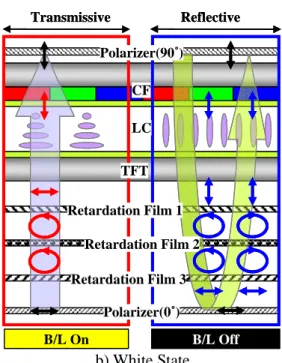
Fig 1. Transmissive/reflective alteration diagram. In transissive mode, when B/L is On, normal TN Mode is applied and when B/L is Off, reflective mode should be applied along with Data Inversion. (Application to IPS and VA modes is also possible).
Fig 1. shows the principle of how transmissive/reflective modes work in each balck and white state for TN mode Panel. This principle can be applied to IPS and VA modes as well. Transmissive mode uses B/L as the light source in indoor. In reflective mode, however, B/L turns off and inverted voltage is applied so that luminace of light from outside can be adjusted. Light from outside in reflective mode black state gets linearly polarized by the upper polarizer, and as it passes through the cell it gets polarized by 90˚. Through the retardation films it reaches the reflective polarizer and then it reflects back to the upper polarizer where it gets absorbed away and appear as black state. Whereas in white state light form outside maintains its linear polarization state all the way without being absorbed.
The retardation film 1and 3 has Rin value of 100~150nm and the retadation film 2 has selective reflector function in which 3M’s DBEF and CLC(Cholesteric Liquid Crystal) are used. In order to avoid rainbow mura caused by retardation films stacking up, optimization of haze between the films can be done.
In this experiment, white LED backlight was used and resolution of 1024 × 600 and 10.1 inch prototype sample was provide. Also combination of high reflective and clear CLC Films and QWP Films was used in the anlaysis as the reflective polarizer.
3. Results and discussion
Table 1. represents data collected in an experiment where 2 types of QWP retardation films according to the haze level are tested for each transmissive and reflective mode. Transmittances in T-mode were the same and CR varied depending on haze level. A-1 type showed the best result. This, we believe, is because of the fact that haze beads scattering the light brought about depolarized and deviation of the polarization axis caused by hand work influenced transmittance. In R-mode, B type was the best out of the others and we expect further improvement by the optimization of the retardation value.
TABLE 1. Periodic table of elements
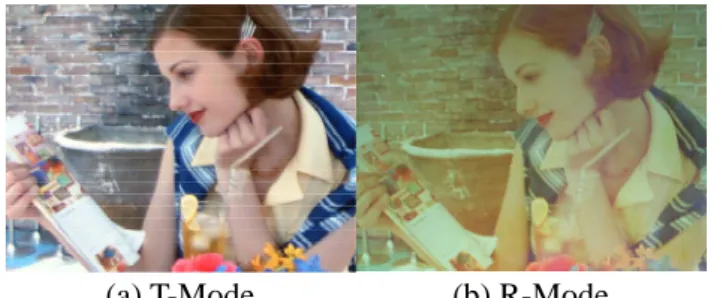
Fig 2. is B type retardation film applied 10.1 inch prototype sample where left hand side is T-mode and right hand side is R-mode. In R-mode, 2000lux of light was shone. Our assumption is that in genuine outdoor condition better performance is expected. In addition, to enhance the reflection more, increase in panel transmittance is important. This is possible via retardation modification and haze level control in QWP and CLC and this improvement was verified.
We have also confirmed that in R-mode power consumption was lowered more than 85% over T-mode. Reflective Transmissive Polarizer(90˚) Polarizer(0˚) CF LC Retardation Film 1 Retardation Film 2 Retardation Film 3 TFT B/L On B/L Off Reflective Transmissive Polarizer(90˚) Polarizer(0˚) CF LC Retardation Film 1 Retardation Film 2 Retardation Film 3 TFT B/L On B/L Off Excellent Poor Fair Tnickness Excellent Fair Excellent Reflective CR @Spot (30/10) Excellent Poor Fair Reflecance R-Mode Fair Fair Excellent CR Fair Fair Fair Transmittance T-Mode B type (Hz 60%) A-2 type (Hz 60%) A-1 type (Hz 40%) Excellent Poor Fair Tnickness Excellent Fair Excellent Reflective CR @Spot (30/10) Excellent Poor Fair Reflecance R-Mode Fair Fair Excellent CR Fair Fair Fair Transmittance T-Mode B type (Hz 60%) A-2 type (Hz 60%) A-1 type (Hz 40%)
P1-23 / Y. J. Kim
IMID 2009 DIGEST •
(a) T-Mode (b) R-Mode
Fig. 2. Image according to Transmissive/Reflective Mode Switching.(a) Transmissive, (b) Reflective.
4. Summary
In this paper, we proved that alternation between transmissive and reflective mode is achievable without adjustment in aperture ratio. The fact that panel design and modification of cell and retardation value of reflective polarizer is crucial so as to gain a fine quality trans-flective display.
5. References
1. S. Komura, et al., SID vol. 5/3, pp.261(1997). 2. O. Itou, et al., SID’06 Digest, P-231L, p.832(2006). 3. N. Aoki, SID’06 Digest, 16-3, p.1087(2006).. 4. N. Koma, et al., SID’07 Digest,35-3,p.1270(2007). 5. Y. Y. Fan, et al., SID’04 Digest,P-101,p.6470(2004).