Highly transparent organic light-emitting diodes
with a metallic top electrode: the dual role of a
Cs
2
CO
3
layer
Hyunsu Cho, Jung-Min Choi, and Seunghyup Yoo*
Department of Electrical Engineering, Korea Advanced Institute of Science and Technology (KAIST),373-1 Guseong-dong, Daejeon 305-701, South Korea
Abstract: Highly transparent organic light-emitting diodes (TrOLEDs) are demonstrated using damage-free top cathodes of Cs2CO3/ Ag capped with ZnS layers. The presence of ultrathin Cs2CO3 layers not only improves the electron injection properties but also makes Ag thin films more continuous and uniform, resulting in ideal top electrodes with low sheet resistance and high transmittance. The combination of the uniform Ag morphology enabled by Cs2CO3 and the optimized thickness of ZnS capping layers results in TrOLEDs that have a peak transmittance as large as 80% with a luminous transmittance of 76.4%. These TrOLEDs exhibit a low turn-on voltage of 2.6V due to injection improvement by the Cs2CO3 layers.
©2011 Optical Society of America
OCIS codes: (230.3670) Optical devices: Light-emitting diodes; (230.4170) Optical devices: Multilayer; (310.6845) Thin films: Thin film devices and applications; (310.6860) Thin films; Thin films, optical properties.
References and links
1. G. Gu, V. Bulovic, P. E. Burrows, S. R. Forrest, and M. E. Thompson, “Transparent organic light emitting devices,” Appl. Phys. Lett. 68(19), 2606–2608 (1996).
2. G. Parthasarathy, P. E. Burrows, V. Khalfin, V. G. Kozlov, and S. R. Forrest, “A metal-free cathode for organic semiconductor devices,” Appl. Phys. Lett. 72(17), 2138–2140 (1998).
3. A. Yamamori, S. Hayashi, T. Koyama, and Y. Taniguchi, “Transparent organic light-emitting diodes using metal acethylacetonate complex as an electron injective buffer layer,” Appl. Phys. Lett. 78(21), 3343–3345 (2001). 4. H.-K. Kim, K.-S. Lee, and J. H. Kwon, “Transparent indium zinc oxide top cathode prepared by plasma
damage-free sputtering for top-emitting organic light-emitting diodes,” Appl. Phys. Lett. 88(1), 012103 (2006). 5. S. Y. Ryu, S. H. Choi, J. T. Kim, C. S. Kim, H. K. Baik, and H. S. Jeong, “Highly efficient transparent organic
light-emitting diodes by ion beam assisted deposition-prepared indium tin oxide cathode,” Appl. Phys. Lett. 90(3), 033513 (2007).
6. R. B. Pode, C. J. Lee, D. G. Moon, and J. I. Han, “Transparent conducting metal electrode for top emission organic light-emitting devices: Ca-Ag double layer,” Appl. Phys. Lett. 84(23), 4614–4616 (2004).
7. Z. Xie, L.-S. Hung, and F. Zhu, “A flexible top-emitting organic light-emitting diode on steel foil,” Chem. Phys. Lett. 381(5-6), 691–696 (2003).
8. S. Kim, K. Hong, K. Kim, I. Lee, K.-B. Kim, D. Y. Lee, T.-Y. Kim, and J.-L. Lee, “Hole injection layer of thermally evaporated copper oxide for top emitting organic light emitting diodes,” J. Electrochem. Soc. 157(10), J347–J350 (2010).
9. D.-D. Zhang, J. Feng, Y.-Q. Zhong, Y.-F. Liu, H. Wang, Y. Jin, Y. Bai, Q.-D. Chen, and H.-B. Sun, “Efficient top-emitting organic light-emitting devices using Fe3O4 modified Ag anode,” Org. Electron. 11(12), 1891–1895 (2010).
10. B. J. Chen, X. W. Sun, and S. C. Tan, “Transparent organic light-emitting devices with LiF/Mg:Ag cathode,” Opt. Express 13(3), 937–941 (2005).
11. T. Zhang, L. Zhang, W. Ji, and W. Xie, “Transparent white organic light-emitting devices with a LiF/Yb:Ag cathode,” Opt. Lett. 34(8), 1174–1176 (2009).
12. H. Riel, S. Karg, T. Beierlein, B. Ruhstaller, and W. Rieß, “Phosphorescent top-emitting organic light-emitting devices with improved light outcoupling,” Appl. Phys. Lett. 82(3), 466–468 (2003).
13. T.-W. Koh, J.-M. Choi, S. Lee, and S. Yoo, “Optical outcoupling enhancement in organic light-emitting diodes: highly conductive polymer as a low-index layer on microstructured ITO electrodes,” Adv. Mater. 22(16), 1849– 1853 (2010).
14. T. Hasegawa, S. Miura, T. Moriyama, T. Kimura, I. Takaya, Y. Osato, and H. Mizutani, “Novel electron-injection layer for top-emission OLEDs,” SID Int. Symp. Digest Tech. Papers 35(1), 154–157 (2004).
#138493 - $15.00 USD Received 24 Nov 2010; revised 23 Dec 2010; accepted 23 Dec 2010; published 10 Jan 2011
15. G. Li, C.-W. Chu, V. Shrotriya, J. Huang, and Y. Yang, “Efficient inverted polymer solar cells,” Appl. Phys. Lett. 88(25), 253503 (2006).
16. D. Poitras, C.-C. Kuo, and C. Py, “Design of high-contrast OLEDs with microcavity effect,” Opt. Express 16(11), 8003–8015 (2008).
17. X. Liu, X. Cai, J. Qiao, J. Mao, and N. Jiang, “The design of ZnS/ Ag/ ZnS transparent conducive multilayer films,” Thin Solid Films 441(1-2), 200–206 (2003).
18. B. P. Rand, P. Peumans, and S. R. Forrest, “Long-range absorption enhancement in organic tandem thin-film solar cells containing silver nanocluster,” J. Appl. Phys. 96(12), 7519–7526 (2004).
19. N. Kaiser, “Review of the fundamentals of thin-film growth,” Appl. Opt. 41(16), 3053–3060 (2002). 20. H. Cho, C. Yun, and S. Yoo, “Multilayer transparent electrode for organic light-emitting diodes: tuning its
optical characteristics,” Opt. Express 18(4), 3404–3414 (2010).
21. B. O’Connor, C. Haughn, K.-H. An, K. P. Pipe, and M. Shtein, “Transparent and conductive electrodes based on unpatterned, thin metal films,” Appl. Phys. Lett. 93(22), 223304 (2008).
22. S. Chen, Z. Jie, Z. Zhao, G. Cheng, Z. Wu, Y. Zhao, B. Quan, S. Liu, X. Li, and W. Xie, “Improved light outcoupling for top-emitting organic light emitting devices,” Appl. Phys. Lett. 89(4), 043505 (2006). 23. H. A. Macleod, Thin-film optical filters (Taylor & Francis, 2001).
24. J. Meiss, M. K. Riede, and K. Leo, “Optimizing the morphology of metal multilayer films for indium tin oxide(ITO)-free inverted organic solar cells,” J. Appl. Phys. 105(6), 063108 (2009).
25. C.-I. Wu, C.-T. Lin, Y.-H. Chen, M.-H. Chen, Y.-J. Lu, and C.-C. Wu, “Electronic structures and electron-injection mechanisms of cesium-carbonate-incorporated cathode structures for organic light-emitting devices,” Appl. Phys. Lett. 88(15), 152104 (2006).
26. J. Huang, Z. Xu, and Y. Yang, “Low-work-function surface formed by solution-processed and thermally deposited nanoscale layers of cesium carbonate,” Adv. Funct. Mater. 17(12), 1966–1973 (2007).
27. D. Han, H. Kim, S. Lee, M. Seo, and S. Yoo, “Realization of efficient semitransparent organic photovoltaic cells with metallic top electrodes: utilizing the tunable absorption asymmetry,” Opt. Express 18(S4), A513–A521 (2010).
1. Introduction
One of the many advantages of organic light emitting diodes (OLEDs) over other types of displays is that they can be easily adapted to transparent displays [1]. Considering the typical structure of OLEDs, which consist of a transparent anode of indium tin oxide (ITO) film, thin organic layers, an inorganic buffer layer (optional), and a metallic cathode, transparent OLEDs (TrOLEDs) with the most straightforward structure would be those in which the metallic cathode is replaced with ITO or similar transparent conductive oxides (TCO) [2, 3]. However, the deposition process of ITO or common TCOs, based mostly on RF sputtering, can damage the underlying organic layers. This sputtering damage may be alleviated to some degree by using a buffer layer, but complete protection is still regarded as challenging. Moreover, obtaining highly transparent TCOs with high conductivity often requires a high-temperature annealing process [4, 5] that is inapplicable to OLEDs due to the relatively low service temperature of organic materials. Another candidate that can be relatively free from deposition-induced damage is semitransparent thin metal layers deposited by thermal evaporation. They have been used as a top electrode typically in top-emission OLEDs [6–9] and also in transparent OLEDs (TrOLEDs) [10, 11], often in association with a buffer layer for injection improvement. In TrOLEDs using a metal top electrode, however, obtaining a high transmittance is challenging due to the relatively large reflection and absorption of metallic thin films. Reflection from a metal electrode may be reduced to a certain degree by the appropriate use of a capping layer [12], but absorption has not been easy to suppress. Hence the transmittance of TrOLEDs with a metal top electrode has been typically below 60-70% at best. In this work, we present a combinatorial approach that can reduce both the reflection and absorption of a thin silver layer and, at the same time, can improve its sheet conductance as well as its electron injection properties, so as to realize efficient, highly transparent OLEDs. In particular, emphasis is given to a thermally evaporated thin Cs2CO3 layer that plays a dual role as the electron injection layer and the nucleation-promoting layer for Ag.
2. Experiment
The proposed TrOLEDs are based on a conventional multilayer geometry using N,N'-bis(naphthalen-1-yl)-N,N'-bis(phenyl)-benzidine (NPB) as the hole-transporting layer (HTL) and tris(8-hydroxy-quinolinato) aluminum (Alq3) as the emission/ electron-transporting layer
#138493 - $15.00 USD Received 24 Nov 2010; revised 23 Dec 2010; accepted 23 Dec 2010; published 10 Jan 2011
(EML/ETL). ITO glass substrates were cleaned in an ultrasonic bath and treated by air plasma using a plasma cleaner (PDC-32G, Harrick Plasma) prior to deposition of the organic materials [13]. Optional Cs2CO3 layers with a nominal thickness of 1.5 nm were deposited on top of the Alq3 layers primarily for an electron-injecting layer (EIL). Ag layers with a thickness in the range of 9-15nm were used as the top cathode. The Cs2CO3 layers was chosen because ultrathin Cs2CO3 layer had recently been shown to work as an electron injecting/ collecting buffer layer in both OLEDs [14] and organic solar cells [15]. In contrast to a common EIL of LiF, which is known to work rather exclusively with Al, Cs2CO3 layers were shown to work comparably well with Al, Ag, and ITO [14, 15], indicating that the effectiveness of Cs2CO3 layers is relatively insensitive to the choice of a metal layer used together. Such insensitiveness can be beneficial in that a choice of a metal electrode does not need to be limited by the injection capability of the metal itself and thus one can focus more on other aspects such as optical transparency and sheet conductance. Some devices had an additional layer of thermally evaporated ZnS (Alfa Aesar, 99.99%) as an optical capping layer. The current density-voltage-luminance (J-V-L) characteristics of the TrOLEDs were measured in an N2-filled glove box directly connected to the thermal evaporation chamber using a source-measure unit (Model 2400, Keithley), a calibrated photodiode (FDS100-CAL, Thorlab), and a fiber-optic spectrometer (EPP-2000-UV-VIS-NIR, StellarNet). The transmittance was measured with a UV-VIS spectrometer (SV2100, K-MAC). The morphology of the top Ag layer was analyzed using scanning electron microscopy (SEM) (Nova NanoSEM 230, FEI Company) and its optical constant was characterized using the spectroscopic ellipsometer (M2000D, Woollam). For a fair comparison, samples with Ag films used for basic characterizations were prepared in the same batch as the OLED devices. 3. Results and discussions
3.1 Improving the transmittance and sheet conductance of Ag thin films: the role of a Cs2CO3
layer as a nucleation promoter
To realize highly transparent OLEDs with a metal top electrode, it is crucial to first minimize the absorption from the metallic layer. Absorption from a metal layer being proportional to the product of refractive index (n) and extinction coefficient (k), Ag and Au are the most preferred choice due to their relatively low n and k values [16]. In principle, absorption below 5% could be achieved with 15-nm-thick Ag layers. However, the optical properties of metallic layers in this thickness range can be highly dependent on the microscopic morphology of the films. Before metal layers become thick enough to exhibit uniform, continuous morphologies, the effect of scattering and surface plasmon resonance on their optical constants can be significant [17, 18]. With Ag, scattering has been shown to mainly increase n [17], and surface plasmon resonance has been shown to mainly increase k [18]. Note that the nk-product and thus absorption are increased in both cases with respect to that of films with a continuous morphology, which may be described by the optical constants of bulk Ag. It is noteworthy that the critical thickness (dcritical) at which a metal layer begins to exhibit continuous morphologies can differ depending on the conditions of the surface onto which the metal layer is deposited. Hence the morphology of a metal layer needs to be identified on a case-by-case basis and has to be improved, if possible, in order to achieve the maximal transmittance that can be offered by the given metal.
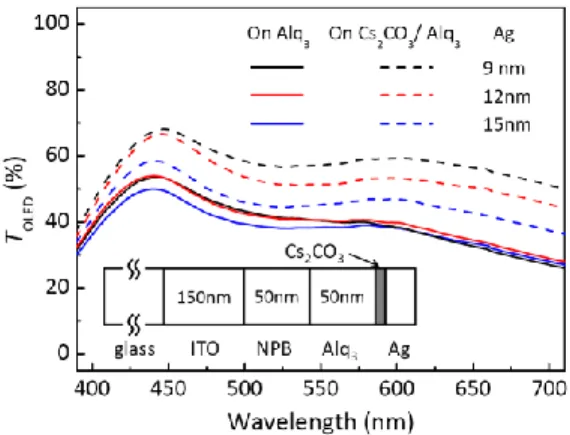
Figure 1 shows the transmittance of OLED devices (= TOLED) with the structure of ITO/ NPB (50nm)/ Alq3 (50nm)/ x/ Ag (9, 12, and 15nm) with x being either Cs2CO3 (1.5nm) or nothing. With a Cs2CO3 layer, TOLED increases as the thickness of the Ag layer (= dAg) decreases, as expected for bulk-like, uniform thin films. Without a Cs2CO3 layer, however, TOLED varies little with dAg. In particular, TOLED values of devices with 9-nm and 12-nm-thick Ag layers are virtually identical within the error bound. This strongly suggests that the overall transmission of the devices without the Cs2CO3 layers is limited by the morphological imperfections of the Ag layers.
#138493 - $15.00 USD Received 24 Nov 2010; revised 23 Dec 2010; accepted 23 Dec 2010; published 10 Jan 2011
Fig. 1. Transmittance of a device with the structure of ITO/ NPB (50nm)/ Alq3 (50nm)/ x/ Ag
(9, 12, and 15 nm) with x being either Cs2CO3 (dash) or nothing (line).
The scanning electron microscopy (SEM) images of Ag layers shown in Fig. 2 confirm that Ag films deposited directly on Alq3 layers exhibit morphologies with more grain boundaries than those deposited on the Cs2CO3 layer. With 9-nm-thick Ag films, both cases show grainy morphologies, but those grown on Cs2CO3/ Alq3 shows morphologies with larger grains and less grain boundaries than those grown on Alq3 layers. With 12-nm-thick Ag films, the difference becomes much more significant: Ag layers grown on Cs2CO3-covered Alq3 layers exhibit compact, uniform morphologies virtually free of grain boundaries while those grown directly on bare Alq3 layers still exhibit grainy features, confirming the importance of Cs2CO3 layers in growing high-quality Ag films. The feasibility of using seed layers that improve wetting to result in continuous thin metal films has been well recognized by Kaiser, and the role of Cs2CO3 layers may be understood in the same context [19].
Fig. 2. The scanning electron microscopy (SEM) images for the top surface of Ag electrodes in OLEDs shown in the inset in Fig. 1(a) either with or without Cs2CO3 for two different Ag
thicknesses of 9 nm and 12 nm.
Figure 3(a) presents the optical constants (n, k) of 15-nm-thick Ag films measured using the spectroscopic ellipsometry. From the practical perspectives of OLED device fabrication, relatively thick Ag layers are preferred, and thus the study hereafter is focused on the optical properties of 15-nm-thick Ag films. It can be seen in Fig. 3(b) that the transmittance calculated using the measured (n, k) values shows quantitative agreement with the measured transmittance of 15-nm-thick Ag films grown on Alq3 and on Cs2CO3/ Alq3. It is noted that
#138493 - $15.00 USD Received 24 Nov 2010; revised 23 Dec 2010; accepted 23 Dec 2010; published 10 Jan 2011
both n and k values are higher for Ag films grown on Alq3 than those on Cs2CO3/ Alq3 in most of the wavelength range studied. In particular, the difference in refractive indices (n) is more significant than that in extinction coefficients (k), indicating that the scattering effect is more dominant than the effect of surface plasmon resonances in the Ag films under study. The latter is known to be more significant when Ag films are composed of numerous island-like aggregates of silver atoms [18, 20]. Since the Ag films under investigation do not show island-like morphologies in all cases, the surface plasmon effect is expected to be weak.
Fig. 3. (a) The optical constant of the 15-nm Ag on Cs2CO3/ Alq3 or Alq3. (b) Measured and
calculated transmittance of the 15nm-thick Ag on x/ Alq3 (50nm)/ glass with x either being
Cs2CO3 (triangle) or nothing (square).
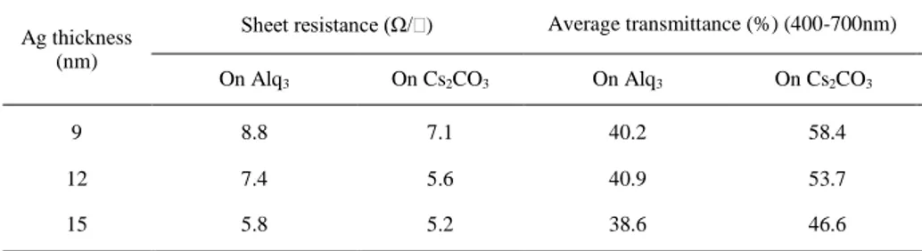
From the practical point of view, successful transparent electrodes should not only exhibit a high transmittance but also have a high sheet conductance (GSH), or equivalently, a low sheet resistance (RSH). As shown in Table 1, RSH values of Ag films on Cs2CO3/ Alq3 are also smaller in all cases than those of Ag films deposited directly on Alq3. For example, RSH of the 12-nm-thick Ag film on Cs2CO3/ Alq3 is as low as 5.6 Ω/sq., while that of the 12-nm-thick Ag film on Alq3 is 7.4 Ω/sq.. This result is consistent with the trend observed in TOLED and SEM experiments in that the scattering of carriers at grain boundaries induces a larger effective resistivity in thin films than those expected for bulk materials of the same kind [21].
Table 1. The effect of the Cs2CO3 layer on sheet resistance of Ag layers and TOLEDa
Ag thickness (nm)
Sheet resistance (Ω/) Average transmittance (%) (400-700nm)
On Alq3 On Cs2CO3 On Alq3 On Cs2CO3
9 8.8 7.1 40.2 58.4
12 7.4 5.6 40.9 53.7
15 5.8 5.2 38.6 46.6
a The OLEDs in a structure shown in the inset of Fig. 1.
From the series of experimental results mentioned above, we can recognize that the Cs2CO3 layer acts as a nucleation-promoting layer that reduces dcritical, thus leading to Ag films with both high transparency and low sheet resistance even at relatively low nominal thickness.
3.2 Further enhancement in the transmittance of transparent OLEDs by high-index capping layers
Once the absorption by a metal layer is suppressed as discussed in the previous section, the reflectance has to be minimized to further enhance TOLED. In modulating the transmittance of
#138493 - $15.00 USD Received 24 Nov 2010; revised 23 Dec 2010; accepted 23 Dec 2010; published 10 Jan 2011
metal-based transparent electrodes, dielectric capping layers have been popular for their simplicity [12, 22]. The overall TrOLED structure with such a capping layer shown in the inset of Fig. 1a may be considered as a dielectric-metal-dielectric (DMD) structure as a whole in which the organic layers and ITO layers below its metal layer can be viewed effectively as a single dielectric layer. In a DMD structure, the right combination of the thicknesses of its two dielectric layers can result in matching of the optical admittance between the DMD multilayer stacks and the ambient medium, leading to a so-called “zero-reflection” condition [17, 23]. Because such a condition is met only at a specific wavelength, however, the average quantity weighted for the human photopic response is typically adopted as an optimization key. We adjusted the thickness of the capping layer or the outer dielectric layer (= dcap) so that it maximized the luminous transmittance (Tlum) of OLEDs defined by
OLED cap photopic lum cap photopic ( ; ) ( ) ( ) ( ) T d f d T d f d
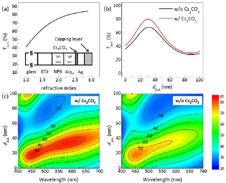
(1)where fphotopic(λ) is the photopic luminosity function given at a wavelength λ [17]. It has to be noted that the maximum Tlum achievable with optimized dcap can be further improved if a dielectric material with a higher n is used for the capping layer [See Fig. 4(a)]. With this in mind, ZnS, having an n of 2.2-2.4, was chosen as a capping layer in this study [22].
Fig. 4. (a) Calculated values for maximum Tlum achievable upon optimization of a capping
layer thickness vs. the refractive index of the capping layer. (b) Calculated Tlum of TrOLEDs
with or without Cs2CO3 layers vs. the thickness of the ZnS layer (dZnS) used as the capping
layer. (c) Contour plots for the calculated TOLED of the same device with or without Cs2CO3
layers as a function of dZnS and wavelength.
Figure 4(b) shows the calculated Tlum for TrOLEDs containing a ZnS capping layer as a function of the thickness of the ZnS layer (= dZnS). It is noted that Tlum of TrOLEDs with the Cs2CO3 layer can be in the range of about 70 - 80% when dZnS is between 20 nm and 42 nm. Without a Cs2CO3 layer, the highest Tlum achievable with the optimal dZnS is smaller by ~15% than that achievable in devices with a Cs2CO3 layer. Figure 4(c) presents the contour plots of TOLED as a function of both λ and dZnS for TrOLEDs with or without Cs2CO3 layers. TOLED greater than ~70% can be obtained at a dZnS of 30±10 nm over a wide spectral range in the
#138493 - $15.00 USD Received 24 Nov 2010; revised 23 Dec 2010; accepted 23 Dec 2010; published 10 Jan 2011
presence of Cs2CO3 layers, while such a high TOLED(λ) is obtained only within a limited spectral range in devices without Cs2CO3 layers, which explains the difference in Tlum in those devices.
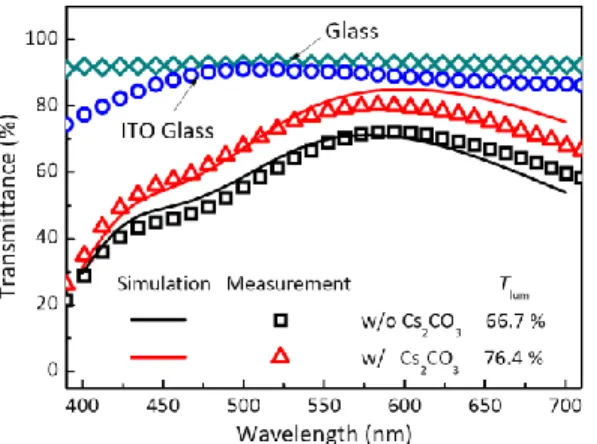
Figure 5 presents the transmittance spectra of actual OLEDs fabricated with 37-nm-thick ZnS-capping layers. It is clear that the experimental data are in a quantitative agreement with the calculation result. Using Eq. (1), Tlum of 76.4% is estimated for the device having both Cs2CO3 and ZnS layers, while Tlum of 66.7% is estimated for the device having a ZnS layer but no Cs2CO3 layer. Along with the calculation results outlined in Fig. 3, this result demonstrates the validity of the proposed combinatorial method based on a nucleation-promoting Cs2CO3 layer and a ZnS capping layer, in which the former suppresses absorption and the latter minimizes the reflection from the Ag layer.
Fig. 5. Measured and calculated transmittance (T) of TrOLED devices in a structure of ITO/ NPB (50nm)/ Alq3 (50nm)/ x/ Ag (15nm)/ ZnS (37nm) with x being either Cs2CO3 (1.5nm)
(triangle) or nothing (square). T of a glass substrate (diamond) and ITO-coated glass substrate (circle) are also presented for comparison.
3.3 Device characteristics of the proposed transparent OLEDs (TrOLEDs)
Transparent electrodes used in OLEDs have to fulfill the requirements for carrier injection as well as those for transmittance and sheet conductance. It is often challenging to satisfy those requirements all at the same time. For example, ultrathin Al was shown to improve the morphology of Ag thin films and thus GSH [24], but it might not be so effective for transparent devices due to the relatively high light absorption of Al. Other multilayers or composite electrode structures such as Ca/Ag or Mg: Ag that are used for better electron injection also suffer from similar problems with limited transmittance. A Cs2CO3 layer was previously shown to enhance electron injection due to highly effective n-doping effect near the organic/ Cs2CO3 interface [25], and thus it may be regarded as an ideal candidate for a layer that can help injection of the desired carriers and, at the same time, can promote formation of uniform Ag layers as shown in the previous section. (For further details on the mechanism of electron injection enhancement by Cs2CO3, please refer to the work by Wu et al. [25] and Huang et al. [26])
Comparison of J-V characteristics of TrOLED devices with or without the 1.5-nm-thick Cs2CO3 layer indeed confirms that electron injection is greatly improved upon insertion of the Cs2CO3 layer [Fig. 6(a)]. Clearly, the J-V curve of the devices with the Cs2CO3 layer is shifted toward a lower voltage by approximately 4V with respect to that of the devices without it. Figure 6(b) presents the luminance (L) - voltage (V) characteristics of a device in a geometry of glass/ ITO/ NPB (50nm)/ Alq3 (50nm)/ Cs2CO3 (1.5nm)/ Ag (15 nm)/ ZnS (37 nm or nothing) for both top and bottom emission directions. One can easily see that the electron injection enhancement due to the Cs2CO3 layer leads to a low turn-on voltage (VT; defined as a voltage for L of 1 cd/m2) of 2.6V, which is comparable to the VT of conventional OLEDs in a configuration of glass/ ITO/ NPB (50nm)/ Alq3 (50nm)/ LiF/Al [20].
#138493 - $15.00 USD Received 24 Nov 2010; revised 23 Dec 2010; accepted 23 Dec 2010; published 10 Jan 2011
Fig. 6. (a) Current density-voltage (J-V) of the TrOLED according to the presence of the Cs2CO3 layer and (b) luminance-voltage (L-V) characteristics of the TrOLED with the Cs2CO3
layer for bottom (ITO side) and top (Ag side) emission according to the presence of a 37-nm-thick ZnS layer. Inset in (a) is a photograph of the TrOLED with a pixel turned on.
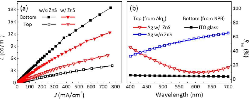
The TrOLED device with both ZnS and Cs2CO3 layers exhibits luminous efficacy ηcd of 2.3 cd/A for ITO-side emission and 1.2 cd/A for Ag-side emission, respectively. (See Fig. 7(a)) Note that the luminous efficacy for the total emission is 3.5 cd/A, which is also comparable to the conventional NPB/ Alq3-based OLEDs [20]. The asymmetry in ηcd, observable in Figs. 6(b) and 7(a), is considered to come from the finite internal reflection of the generated light from the Ag layer and is a phenomenon characteristic of TrOLEDs containing a metal-based electrode on one side and an ITO or similar transparent electrode on the other side. A degree of asymmetric light-emission may be tuned by varying dZnS depending on the requirements of the target application, as we demonstrated in semitransparent organic solar cells [27]. As shown in Fig. 7(b), dZnS of 37nm, which almost maximizes Tlum, corresponds to a situation in which the internal reflection (Rint) at the organic/ Ag interface is suppressed to yield an emission that is relatively well balanced for both directions.
Fig. 7. (a) Luminance-current density (L-J) characteristics of the TrOLED with a Cs2CO3 layer
for the bottom (ITO side, filled) and top (Ag side, open) emission according to the presence of a 37-nm-thick ZnS. (b) Spectra of internal reflectance (Rint) at the organic/ Ag interface (open)
and the organic/ ITO interface (closed).
Hence, changing dZnS to enhance the emission in a certain preferred direction would require a compromise in Tlum to some degree. A good example is in fact the light emission characteristics of a TrOLED device without the ZnS layer. This device does have a relatively high Rint as Fig. 7(b) shows, to yield a highly asymmetric light emission in which ITO-side emission is enhanced as Fig. 7(a) shows at the cost of a reduced Tlum. [Recall that the Tlum of TrOLEDs without ZnS layers is limited to approximately 40%.]
#138493 - $15.00 USD Received 24 Nov 2010; revised 23 Dec 2010; accepted 23 Dec 2010; published 10 Jan 2011
4. Conclusions
We proposed a strategy for highly transparent OLEDs based on a combinatorial approach using a ZnS layer as a high-index capping layer and a Cs2CO3 interlayer as a nucleation-promoter and an electron injection layer. The former effectively enhances the transmittance of OLEDs by suppressing reflectance with appropriate optimization of thickness. The latter helps form a uniform, continuous Ag film even at a low nominal thickness, suppressing the absorption and thus improving the overall transmittance. The latter also helps to mitigate the scattering-induced decrease in sheet conductance of the Ag thin films, eventually to enable the Ag layers to have both high transparency and low sheet resistance. With the proposed method, we demonstrated efficient transparent OLEDs having a luminous transmittance of 76.4% and peak transmittance of 80%. The origin of the observed asymmetric light emission in the proposed TrOLEDs was also discussed including its relation to the luminous transmittance. We believe the work presented here provides a logical route to develop highly transparent OLEDs based on a metal-based top electrode, which has advantages over ITO electrodes due to its large-area compatibility and damage-free nature.
Acknowledgment
This work was supported by the Technology Innovation Program (10035573, Development of selective transparent displays through innovation in device structure) funded by the Ministry of Knowledge Economy (MKE, Korea).
#138493 - $15.00 USD Received 24 Nov 2010; revised 23 Dec 2010; accepted 23 Dec 2010; published 10 Jan 2011