INTRODUCTION
In past years, radiation detection systems were developed at many research institutes and academies in the Republic of Korea. In addition, most radiation detection systems includ-ing radiation detectors are imported. To concentrate and in-dustrialize these scattered radiation detector technologies, the research infrastructure was expected to be established at a national level to increase the national competitive edge. The development of radiation detectors has also changed from a gas-filled detector into a solid-state detector based on compound semiconductors owing to their merits such as high atomic number, high density, room temperature opera-tion, and direct coupling with electronics (Knoll 1999). In a planned infrastructure, crystal growth and a compound
semi-conductor fabrication process, which are bottleneck-tech-nologies in the development of radiation detection systems, are scheduled to be developed and to support industrial cir-cles. In this paper, the planned facility, equipment, and their utilization for radiation detector fabrication are introduced. The application fields of radiation detectors are also briefly addressed.
ESTABLISHMENT OF RESEARCH
INFRASTRUCTURE FOR RADIATION
DETECTOR
The designated site of the research infrastructure for radia-tion detectors is at the RFT (Radiaradia-tion Fusion Technology) center at KAERI (Korea Atomic Energy Research Institute). Completion of the construction is planned for 2015. The size of the radiation detector fabrication facility is 1,200 m2of the overall research facility (3,300 m2). A bird’s-eye view of the
Journal of Radiation Industry 6 (1) : 67~73 (2012)
─ ─ 67 ──
Research Infrastructure Foundation for Core-technology
Incubation of Radiation Detection System
Han Soo Kim, Jang Ho Ha, Young Soo Kim and Hyung Ki Cha*
Korea Atomic Energy Research Institute, Daejeon 305-353, Korea
Abstract -- The development of radiation detection systems mainly consist of two parts-radiation detector fabrication including material development, and its appropriate electronics development. For the core-technology incubation of a radiation detection system, radiation fabrication and an evaluation facility are scheduled to be founded at the RFT (Radiation Fusion Technology) Center at KAERI (Korea Atomic Energy Research Institute) by 2015. This facility is utilized for the development and incubation of bottleneck-technologies to accelerate the industrialization of a radiation detection system in the industrial, medical, and radiation security fields. This facility is also utilized for researchers to develop next-generation radiation detection instruments. In this paper, the establishment of core-technology development is introduced and its technological mission is addressed.
Key words : Radiation detection system, Crystal growth, Compound semiconductor, Fabrication process, Evaluation facility
* Corresponding author: Hyung Ki Cha, Tel. +82-42-868-2934, Fax. +82-42-861-8292, E-mail. [email protected]
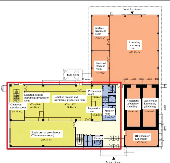
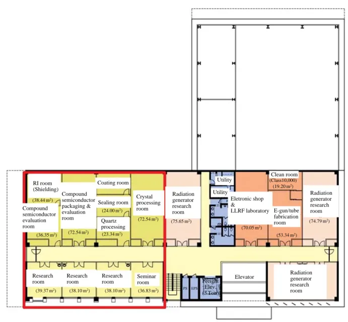
research building is shown in Fig. 1. The research building is shared with the facility for the development of core parts of an electron accelerator. The research infrastructure for the radiation detector mainly consists of a crystal growth facility, a compound semiconductor fabrication process facility, and a performance evaluation facility. The planned layout of the facilities is shown in Figs. 2 and 3. In this section, these facil-ities are introduced in detail.
Crystal growth facility
There has been a drift toward changing scintillators into semiconductor materials owing to their principal superiority. Single crystals, which have a repetitive atomic arrangement in a solid lattice, have excellent chemical and electrical pro-perties. The major proposed candidates for radiation detec-tors materials are CdZnTe, CdTe, TlBr, HgI2, etc. Among these, the CdZnTe semiconductor is the most promising. The major developing scintillators are cerium-doped lanthanum bromide (LaBr3) and halide single crystals. Halide is com-posed of group seven elements in the periodic table such as chlorine (Cl), bromine (Br) and iodine (I). LaBr3is a new compound scintillator for X-ray and gamma-ray detection at room temperature. Recently, LaBr3has been used as a radia-tion detector for nuclear medicine imaging and container in-spection systems. Scintillators based on oxide are also newly developed. Ceramic scinitllators such as cadmium tungstate
(CdWO4), bismuth germinate (Bi4Ge3O12), are Lutetium oxy-orthosilicate (Lu2SiO5) have merits as radiation detectors, such as their scintillation properties, chemical stability, and physical hardness. These newly developing materials desi-gned for development in this facility.
The designated size of the crystal growth facility is 216 m2. It was designed to maintain a constant temperature and humidity to prevent a fluctuation of the outer temperature for crystal growth. The installed equipment and their utiliza-tion are summarized in Table 1.
Compound semiconductor fabrication process facility
Cadmium zinc telluride (CdZnTe), Cadmium telluride (CdTe), mercury iodide (HgI2), and thallium bromide (TlBr) wide band gap semiconductors have attracted increasing in-terest as X-ray and gamma-ray detectors owing to their su-perior physical properties to conventional semiconductors such as silicon and germanium. Radiation detector fabrica-tion using these compound semiconductors cannot be appli-ed in establishappli-ed facilities such as the Nano Fab. Center and ETRI (Electrical and Telecommunication Research Institute) owing to contamination during processing. These facilities were originated to develop electronic devices based on sili-con wafers. These compound semisili-conductors, including sili- con-ventional Si semiconductor detectors, are designed for pro-Fig. 1. A bird’s-eye view of research building for core-technology development of radiation detector and electron beam accelerator.
cessing in this facility.
The designated size of the compound semiconductor
fab-rication process facility is 288 m2. This facility consist of class 100 and class 1,000 clean rooms for the lithography Foundation Construction for Source-technology Incubation of Radiation Detection System 69
Fig. 2. A plan view of research building for core-technology development of radiation detector (red box).
Table 1. Summary of crystal growth equipments and their utilization
Furnace Utilization
Vertical Bridgman Furnace Crystal growth for compound semiconductors
(CdZnTe, CdTe, CdMnTe, ZnS, CdS, ZnSe, ZnTe, CdSe, PbMoO4etc.)
Traveling Heater Furnace Crystal growth for compound semiconductors (CdZnTe, CdTe, CdMnTe, etc.)
Czochroski Furnace Crystal growth for oxide scinitllators (Bi4Ge3O12, CdWO4, Lu2SiO5etc.)
Zone Melting Furnace Purification of compound semiconductors
Vacuum Distillation Furnace Purification of compound semiconductors and scintillators
Sublimation Purification Furnace Purification of compound semiconductors and scintillators
Horizontal 3-zone Furnace Quartz tube preparation etc.
Vehicle entrance Surface treatment room Annealing processing room (78.69 m2) (430.80 m2) (75.79 m2) 2000 1000 1000 13600 1000 4800 1000 4800 1000 (29.84 m2) (18.29 m2) (216.00 m2) PS PS EPS (15.50 m2) (84.68 m2) (79.36 m2) (84.68 m2) (64.48 m2) (Class100) (63.00 m2) (Class1000) (164.49 m2) Precision machine room Radiation sensors instruments production
room Accelerator Accelerator
Laboratory Laboratory (shielding) (shielding) Radiation sensors and
instruments production room
Single crystal growth room (Thermostatic room) Cleanroom machine room Preparation room Preparation room RF generator Laboratory Monitor room Tank room Entrance Elevator Main entrance
Fig. 3. A plan view of research building for core-technology development of radiation detector (red box).
Table 2. Summary of semiconductor process equipments and their utilization
Fabrication process equipment Utilization
Oxidation Furnace Oxidation of semiconductor
Photoresister coater Lithography
Photoresister track system Lithography and inspection
Dry etcher Etching process
Wet etcher Etching process
Oxide etcher Oxide etching process
Horizontal 3-zone Furnace Quartz tube preparation etc.
Plasma-enhanced chemical vapor deposition Thin film formation
Low pressure chemical vapor deposition Thin film formation
Sputter Metallization, Radiation converter deposition
Thermal evaporator Metallization, Radiation converter deposition
Electron beam evaporator Metallization, Radiation converter deposition
Dicing saw Semiconductor cutting
Wire bonder Signal wiring
Flip-chip bonder Pixel-type semiconductor signal extraction
Microscope Inspection RI room (Shielding) (38.44 m2) (24.00 m2) (23.34 m2) (72.54 m2) (75.65 m2) (70.05 m2) (74.79 m2) (53.34 m2) (Class10,000) (19.20 m2) (72.54 m2) (36.35 m2) (39.37 m2) (38.10 m2) (38.10 m2) (36.83 m2) Compound semiconductor evaluation room Crystal processing room E-gun/tube fabrication room Eletronic shop & LLRF laboratory Radiation generator research room Radiation generator research room Radiation generator research room Quartz processing Seminar room PS EPS Research Research Research
room room room
Coating room Sealing room Utility Elevator Freight Elev. (3 Ton) Utility Clean room Compound semiconductor packaging & evaluation room
process and other fabrication processes, respectively. The installed equipments and their utilization are summarized in Table 2.
Performance evaluation facility
The designated size of this facility is 288 m2. This facility is designed for the processing and evaluation of single cry-stals and radiation detectors. The installed equipments and their utilization are summarized in Table 3.
In addition to these three main facilities, sample prepara-tion facilities are also provided as demanded.
APPLICATION FIELDS OF RADIATION
DETECTOR
Conventional radioisotope identifiers, which are equipped with a scintillator detector, are bulky, heavy, and high pow-er consuming. A compact radioisotope identifipow-er, which is equipped with a CdZnTe semiconductor, is a recently devel-oped radiation detector. It has a superior performance such as better energy resolution than a conventional detector. Fig. 4 shows a compact radioisotope identifier. An XRF (X-ray Fluorescence Spectrometer) is an industrial radiation detec-tor used to explore environmental contaminants, which are Foundation Construction for Source-technology Incubation of Radiation Detection System 71
Table 3. Summary of preparation and evaluation equipments and their utilization
Crystal processing and performance evaluation equipment Utilization
Grinding and polishing machine Single crystal processing
Diamond wire Saw Single crystal cutting
Optical Microscope Inspection for single crystal and semiconductor
Optical transmittance measuring system Scintillator, semiconductor transmittance inspection
Probe station Semiconductor characterization
Hole measurement system Semiconductor characterization
Alpha step Thickness measurement for deposited material on semiconductor
Photoluminescence Measurement system Photoluminescence Measurement for semiconductor
X-ray diffraction Crystallization inspection
X-ray fluorescence spectrometer Elemental analysis
Current source Radiation detector and electronics evaluation (Electrical response)
Nuclear instrument modules Radiation detector evaluation (Radiation response)
Oscilloscope Radiation detector and electronics evaluation
Electrometer Radiation detector evaluation
Fig. 4. A conventional radioisotope identifier and recently developed compact radioisotope identifier [Thermo Scientific Corporation, http://
www.thermoscientific.com] (Images from Thermo Scientific Corporation Web pages).
CZT radiation sensor
CZT radioisotope identifier Conventional radioisotope identifier
-mainly composed of heavy meals. In recent years, portable XRF instruments have been developed by virtue of compact X-ray generator and a radiation sensor. A portable XRF is utilized in heavy metal analyses on-site and in soil analyses in space probes. They are also utilized to ascertain the gen-uineness of art works. A portable XRF system is shown in
Fig. 5. A 3D scanner can simultaneously detect and discri-minate organic and inorganic substances. It can also draw these substances through image mapping. This 3D scanner can give 2D image information and simultaneously analyze the composition of substances. This 3D scanner technology has attracted the attention of counter-terrorism industries.
Fig. 5. Portable XRF system and its application [Thermo Scientific Corporation, http://www.thermoscientific.com/Fluke corporation, http://www.
Fluke.com] (Images from Thermo Scientific Corporation and Fluke corporation web pages).
Fig. 6. A 3D scanner and its operation principle [SAIC corporation, http://www.saic.com] (Images form SAIC Corporation web pages).
Silicon drift detector
-X-Rays enter Anti-scatter blades Crystal/Photodi ode assembly
-This is shown in Fig. 6. Other application fields and their extended products using radiation detectors are summarized in Table 4.
CONCLUSION
A radiation fabrication and evaluation facility is scheduled to be founded for core-technology incubation of a radiation detection system. This facility is utilized for the development and incubation of bottleneck-technologies to accelerate the industrialization of radiation detection systems in industrial, medical, and radiation security fields. This facility will be based on and serve for the development of radiation sensor materials, radiation detectors, container inspection systems, radiation therapy systems and so on, which need to be obta-ined for a strategic nation approach. These types of R&D equipments will be selected in view of technical barriers and future market growth. This facility will be a development guide along with a research institute, university, and indus-try. This facility will be an R&D hub combining the human-resources of a university, an infrastructure of a research in-stitute, and the market needs of industry. This facility will
also contribute to the radiation equipment industry through the promotion of technology, and a policy related to provin-cial government participation and long-term construction planning for the industry complex.
ACKNOWLEDGMENT
This work has been carried out under the nuclear R&D program of the Ministry of Education, Science and Technol-ogy (MEST) of Korea.
REFERENCES
Knoll GF. 1999. Radiation detection and measurement. 3th ed. John Wiley and Sons, New York.
Thermo Scientific Corporation, http://www.thermoscientific. com
Fluke corporation, http://www. Fluke.com SAIC corporation, http://www.saic.com
Manuscript Received: February 10, 2012 Revised: February 24, 2012 Revision Accepted: March 6, 2012
Foundation Construction for Source-technology Incubation of Radiation Detection System 73
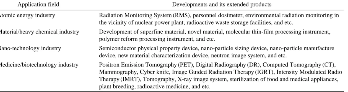
Table 4. Application fields and extended products of radiation detector
Application field Developments and its extended products
Atomic energy industry Radiation Monitoring System (RMS), personnel dosimeter, environmental radiation monitoring in
the vicinity of nuclear power plant, radioactive waste storage facilities, and etc.
Material/heavy chemical industry Development of superfine material, novel material, molecular thin-film processing instrument,
polymer reform processing instrument, and etc.
Nano-technology industry Semiconductor physical property device, nano-particle sizing device, nano-particle manufacture
device, new material characterization device, neutron image system, and etc.
Medicine/biotechnology industry Positron Emission Tomography (PET), Digital Radiography (DR), Computed Tomography (CT),
Mammography, Cyber knife, Image Guided Radiation Therapy (IGRT), Intensity Modulated Radio Therapy (IMRT), Tomography, X-ray image system, sterilization of food and medical appliances, plant breeding, radioactive medicine, and etc.