커패시터 전압 자기 밸런싱 기능이 있는 새로운 6-레벨 인버터 토폴로지
프리바디조나단, 이동춘
영남대학교 전기공학과
A Novel Six-Level Inverter Topology with Capacitor Voltage Self-Balancing
Jonathan Pribadi and Dong-Choon Lee
Department of Electrical Engineering, Yeungnam University ABSTRACT
In this paper, a novel six-level inverter is proposed. Voltage regulation is applied at DC-link and flying capacitors through the implementation of phase-shifted carrier-based modulation with zero-sequence voltage injection. The performance of the proposed structure has been verified under various modulation indices, where low voltage ripple is achieved at each capacitor and total harmonic distortions (THD) of line voltage at unity modulation index is about 15.95%.
1. Introduction
Over past several decades, multilevel converters have attracted wide attentions due to the numerous benefits which are offered, such as lower output voltage steps, reduced harmonic distortions, alleviated electromagnetic interference, and lower voltage stress at switching devices. The widely recognized classical topologies, such as neutral-point clamped inverter (NPC) and flying-capacitor inverter (FCI), have been considered as key enablers to the invention of novel and more advanced
topologies [1]. These recent converters have been developed to obtain
optimum performance in various applications. Numerous advanced hybrid
inverters have also been developed for DC-AC operation [2]–[4]. These
topologies can be seen as derivations of active neutral-point clamped (ANPC) inverters, where one capacitor is added to the neutral point of DC-link. In comparison with the classical flying-capacitor inverter, these topologies require less flying-capacitor sub-circuits in order to obtain the same number of voltage level. However, these topologies require special balancing control to regulate the DC-link capacitor voltages and maintain all flying-capacitor voltages simultaneously. This requirement can be satisfied by either adding external balancing circuit or applying specific modulation techniques. In the former method, more passive and active components are needed, hence the device count is increased.
In this paper, a six-level hybrid flying-capacitor inverter (6L-HFCI) is proposed with capability of capacitor self-balancing. The regulation of all DC-link and flying-capacitor voltages are implemented through the injection of zero-sequence voltage to corresponding reference values. With the proposed topology, low total harmonic distortions (THD) can be achieved at line-to-line voltages. The effectiveness of the proposed structure and operating scheme is verified through simulation results.
2. Operating Principle of Six-Level Hybrid Flying-Capacitor Inverters
2.1 Configuration
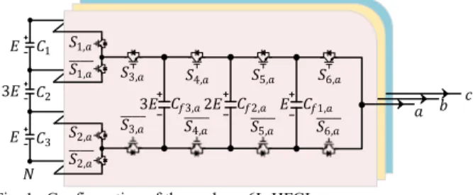
The structure of three-phase 6L-HFCI is shown in Fig. 1. All of phase legs 𝑎, 𝑏, and 𝑐 are fed from the same DC-link capacitor voltage at 𝑉 . If
the base voltage is 𝐸 = 𝑉 ⁄5, the upper and lower capacitors voltages are
set at 𝐸, whereas the middle capacitor voltage is set at 3𝐸. The voltage
stress at each switching device is𝐸.
Each phase in this structure requires three flying-capacitor units with different voltages. The values of capacitances and voltages between two capacitors at the same phase are inversely related. The benefit of employing capacitors which have the same voltage rating can also be obtained by configuring multiple capacitors in series for capacitors with higher voltage,
hence the lower equivalent capacitance.
Unlike the predecessor topology called 6L-HI, the proposed 6L-HFCI
does not require any external DC-link balancing circuit [4]. When
uniformity of devices is prioritized, this topology also demands lower device quantity compared to 6L-NPC and 6L-FCI, as listed in Table I.
2.2 Operating Principle
The selection of switching states and modulation technique should consider the operation with dead-time effect, which can cause undesirable multiple voltage steps. When phase-shifted carrier-based modulation (PS-PWM) is employed, such phenomenon can be avoided since only one gating signal is changed at every switching event. Therefore, dead-time only causes a slight delay at the output voltage.
Under ideal PS-PWM modulation, the reference waveform (𝑣 , ) is
compared with five fixed carrier waves, each of which is shifted 72° from each other. Meanwhile, the output voltage level can be expressed as:
𝑣 = 𝑆, + 𝑆 , + 𝑆 , + 𝑆, + 𝑆, 𝐸, (1)
where 𝑣 represents output phase voltage as a function of the switching
states in the corresponding phase leg. Note that 𝑆, is equal to 𝑆, .
If duty ratios of the aforementioned switches are defined as
𝑑, , 𝑑, , 𝑑 , , 𝑑, , 𝑑, , and 𝑑 , , respectively, the average output
phase voltage over a span of carrier period can be obtained as:
𝑢 = 𝑑, + 𝑑 , + 𝑑, + 𝑑, + 𝑑, 𝐸 = 𝑑 , 𝐸. (2)
In an ideal PS-PWM scheme, where all capacitors voltages are assumed to be balanced, all duty ratios can be considered as constant in a carrier period as follows:
𝑑 , = 5𝑣 , . (3)
To maintain all capacitors voltages, the currents that flow through neutral points and each flying capacitor are controlled by regulating the duty ratio of nearest switches. This control is illustrated in Fig. 2, where zero-sequence voltages (ZSV) are injected to the reference waveform and
𝐸 𝐸 3𝐸 3𝐸 𝑆1,𝑎 𝑆1,𝑎 𝑆2,𝑎 𝑆2,𝑎 𝑆3,𝑎 𝑆6,𝑎 𝑆3,𝑎 𝑆6,𝑎 𝑁 𝑎 𝑏 𝑐 𝐶1 𝐶2 𝐶3 𝐶𝑓1,𝑎 𝑆4,𝑎 𝑆4,𝑎 𝐶𝑓3,𝑎 𝑆5,𝑎 𝑆5,𝑎 𝐶𝑓2,𝑎 2𝐸 𝐸
Fig. 1. Configuration of three-phase 6L-HFCI.
TABLE I. COMPARISON OF SIX-LEVEL INVERTERS
Topologies
Number of Capacitors Number of Active Switches Number of Clamp Diodes Base
Voltage Different Units
6L-FCI 35 13 30 0 6L-NPC 5 5 30 24 6L-HI 11 6 36 0 6L-HFCI 23 12 36 0
316
-전력전자학술대회 논문집 2020. 8. 18 ~ 20implemented through the following equations: ∆𝑣 , = −∆ , −∆ , −∆ , − ∆𝑑 , + ∆𝑑 , , (4) ∆𝑣 , = −∆ , −∆ , −∆ , +∆ , − ∆𝑑 , , (5) ∆𝑣 , = −∆ , −∆ , +∆ , +∆ ,, (6) ∆𝑣 , = − ∆ , +∆ , +∆ , +∆ ,, (7) ∆𝑣 , = ∆𝑑 , + ∆ , +∆ , +∆ ,, (8) 𝑑 , = 𝑣 , + ∆𝑣 , (𝑛 = 2, ⋯ ,6). (9)
This ZSV injection causes divergence at switches duty ratios as illustrated in Fig. 3. Note that the summation of all ZSV components given in (4)-(8) should be equal to zero in order to maintain the same output voltage as that of the initial reference, which can be written as follows:
𝑑𝑠𝑢𝑚,𝑥= 5𝑣𝑟𝑒𝑓,𝑥+
∑
6𝑖=2∆𝑣𝑑𝑖,𝑥∑
6𝑖=2∆𝑣𝑑𝑖,𝑥 = 0 , (10)where the divergence effect on the output voltage is eliminated.
3. Simulation Results
In this section, simulations are performed for the operation of the 6L-HFCI, where the input DC voltage, fundamental frequency, and switching frequency are 7000 V, 60 Hz, and 2000 Hz, respectively. The capacitance of outermost, middle, and innermost flying capacitors are 2 mF, 1 mF, and 0.667 mF, respectively, whereas those of upper, middle, and lower DC-link capacitors are 2 mF, 0.667 mF, and 2 mF, respectively. The load resistance and inductance are 20 Ω and 6 mH, respectively.
The simulation results for pole and line voltages at both high and low amplitude modulation indices are shown in Fig. 4. All capacitor voltages are balanced at the reference values as shown in Fig. 5, where the proposed 6L-HFCI is operated at various modulation indices (𝑚 ). The voltage ripple becomes even lower at lower 𝑚 values.
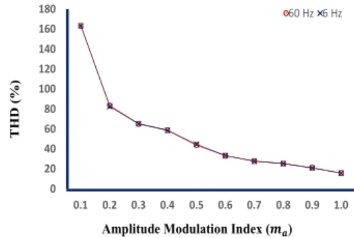
The total harmonic distortions of line-to-line voltages at various amplitude modulation indices are shown in Fig. 6. Note that the values are almost identical for both high and low frequency modulation indices. At unity modulation index, the THD value is 15.95%.
4. Conclusions
In this paper, a novel six-level hybrid flying-capacitor inverter (6L-HFCI) has been proposed. With competitive number of devices, this topology exhibits the capability of self-capacitor voltage balancing without requiring any auxiliary DC-link balancing circuit. The effectiveness of the proposed balancing algorithm has been verified through simulation results, where the THD value at unity modulation index is 15.95%.
References
[1] L. G. Franquelo et al., “Recent advances and industrial applications of multilevel converters,” IEEE Trans. Ind. Electron., vol. 57, no. 8, pp. 2553–2580, 2010, doi: 10.1109/tie.2010.2049719.
[2] Kui Wang, Zedong Zheng, Lie Xu, and Yongdong Li, “A four-level hybrid-clamped converter with natural capacitor voltage balancing ability,” IEEE Trans. Power Electron., vol. 29, no. 3, pp. 1152–1162, 2014, doi: 10.1109/tpel.2013.2262834.
[3] N. D. Dao and D. C. Lee, “Operation and control scheme of a five-level hybrid inverter for medium-voltage motor drives,” IEEE Trans. Power Electron., vol. 33, no. 12, pp. 10178–10187, 2018, doi: 10.1109/TPEL.2018.2811182.
[4] Q. A. Le and D. C. Lee, “A novel six-level inverter topology for medium-voltage applications,” IEEE Trans. Ind. Electron., vol. 63, no. 11, pp. 7195–7203, 2016, doi: 10.1109/TIE.2016.2547909. PI 𝑣𝑓1,𝑥 -+ 𝐸 ∆𝑣𝑓1 ∆𝑑𝑓1,𝑥 signum 𝑖𝑥 ZSV Injection PI 𝑣𝑓2,𝑥 -+ 2𝐸 ∆𝑣𝑓2 PI 𝑣𝐶2 -+ 3𝐸 ∆𝑣𝐶2 PS-PWM 𝑆1,𝑥 𝑆2,𝑥 𝑆3,𝑥 ∆𝑑𝑓2,𝑥 PI 𝑣𝑓3,𝑥 -+ 3𝐸 ∆𝑣𝑓3 ∆𝑑𝐶2,𝑥 𝑆4,𝑥 𝑆5,𝑥 𝑆6,𝑥 ∆𝑑𝑓3,𝑥 PI 𝑣𝐶3 -+ 𝑣𝐶1 ∆𝑣𝐶31 ∆𝑑𝐶31,𝑥
Fig. 2. Control of DC-link and flying-capacitors voltages.
Time D u ty R at io 𝑣𝑟𝑒𝑓 ,𝑥 𝑑1,𝑥 𝑑3,𝑥 𝑑4,𝑥 𝑑5,𝑥 𝑑6,𝑥 ∆𝑣𝑑2,𝑥 ∆𝑣𝑑3,𝑥∆𝑣𝑑4,𝑥 ∆𝑣𝑑5,𝑥 ∆𝑣𝑑6,𝑥 𝑑2,𝑥
Fig. 3. Adjustment of duty ratio with zero-sequence voltage injection for capacitor voltages balancing.
0 V 0 V (a) (b) 𝑣𝑎𝑜 𝑣𝑎𝑏 2 kV/div 0 V 0 V (c) (d) 𝑣𝑎𝑜 𝑣𝑎𝑏 𝑚𝑎 = 0 .9 𝑚𝑎 = 0 .1 20 ms 5 kV/div 2 kV/div 5 kV/div
Fig. 4. Simulation results at 𝑓 = 60 𝐻𝑧. (a) Pole voltage at 𝑚 = 0.9. (b) Line voltage at 𝑚 = 0.9. (c) Pole voltage at 𝑚 = 0.1. (d) Line voltage at 𝑚 = 0.1. 1.38K 1.39K 1.4K 1.41K 1.42Kvf1a vf1b vf1c 2.78K 2.79K 2.8K 2.81K 2.82Kvf2a vf2b vf2c 0 1 2 3 4 5 Time (s) 4.18K 4.19K 4.2K 4.21K 4.22Kvf3a vf3b vf3c 0K -2K -4K -6K 2K 4K 6K Vao-Vbo 1.36K 1.38K 1.4K 1.42K 1.44K Vc_1 Vc_3 0 1 2 3 4 5 Time (s) 4.18K 4.19K 4.2K 4.21K 4.22KVc_2 2 kV/div 𝑣𝑎𝑏 (a) (b) (c) 1.4 kV 4.2 kV 0 V 2.8 kV 4.2 kV 1.4 kV (d) (e) (f) 20 V/div 10 V/div 10 V/div 10 V/div 10 V/div 𝑣𝐶1 𝑣𝐶3 𝑣𝐶2 𝑣𝑓3,𝑥 𝑣𝑓2,𝑥 𝑣𝑓1,𝑥 1 s 0.1 0.3 0.5 0.7 0.9 Various 𝑚𝑎 0.1 0.3 0.5 0.7 0.9 Various 𝑚𝑎 1 s
Fig. 5. Simulation results at various 𝑚 and 𝑓 = 60 𝐻𝑧. (a) Line voltage. (b) DC-link capacitor voltages. (c) Middle DC-link capacitor voltage. (d) Outermost flying-capacitor voltages. (e) Middle flying-capacitor voltages. (f) Innermost flying-capacitor voltages.
T H D ( % ) 0 20 40 60 80 100 120 140 160 180 0.1 0.2 0.3 0.4 0.5 0.6 0.7 0.8 0.9 1.0 60 Hz 6 Hz
Amplitude Modulation Index (𝒎𝒂)
Fig. 6. Total harmonic distortions (THD) of line voltages at various 𝑚 .