Probeless Estimation of Electroluminescence Intensities
Based on Photoluminescence Measurements of GaN-Based
Light-Emitting Diodes
Jongseok Kim1**, Hoon Jeong1, Won-Jin Choi2, and Hyundon Jung3
1Korea Institute of Industrial Technology, Cheonan 31056, Korea 2RayIR Co., LTD., Suwon 16506, Korea
3Etamax Co., LTD., Suwon 16650, Korea
(Received December 29, 2020 : revised January 27, 2021 : accepted February 3, 2021)
The electroluminescence (EL) intensities of GaN-based light-emitting diodes (LEDs) are estimated based on their photoluminescence (PL) properties. The PL intensity obtained under open-circuit con-ditions is divided into two parts: the PL intensity under a forward bias lower than the optical turn-on voltage, and the difference between the PL intensities under open-circuit conditions and under forward bias. The luminescence induced by photoexcitation under a constant forward bias lower than the opti-cal turn-on voltage is primarily the PL from the excited area of the LED. In contrast the intensity dif-ference, obtained by subtracting the PL intensity under the forward bias from that under open-circuit conditions, contains the EL induced by the photocarriers generated during photoexcitation. In addition, a reverse photocurrent is generated during photoexcitation under constant forward bias across the LED, and can be correlated with the PL-intensity difference. The relationship between the photocurrent and PL-intensity difference matches well the relationship between the injection current and EL intensity of LEDs. The ratio between the photocurrent generated under a bias and the short-circuit current is related to the ratio between the PL-intensity difference and the PL intensity under open-circuit conditions. A relational expression consisting of the ratios, short-circuit current, and PL under open-circuit conditions is proposed to estimate the EL intensity.
Keywords : Electroluminescence, Light-emitting diodes, Optical inspection, Photoluminescence OCIS codes : (120.4630) Optical inspection; (230.3670) Light-emitting diodes; (250.5230)
Photoluminescence; (260.3800) Luminescence
*Corresponding author: [email protected], ORCID 0000-0002-5740-2452 Color versions of one or more of the figures in this paper are available online.
This is an Open Access article distributed under the terms of the Creative Commons Attribution Non-Commercial License (http://creativecommons. org/licenses/by-nc/4.0/) which permits unrestricted non-commercial use, distribution, and reproduction in any medium, provided the original work is properly cited.
Copyright © 2021 Current Optics and Photonics
I. INTRODUCTION
Light-emitting diodes (LEDs) have attracted consider-able interest because of their wide range of applications, from general lighting to high-resolution displays [1–3]. For the inspection of LED wafers, photoluminescence (PL) measurements under photoexcitation have been an essential method in industry. Although PL measurements provide considerable information about optical properties [4], the characteristics of LED chips have been examined using chip probers by probing the chip electrodes to evaluate
performance under electrical excitation which matches the LED operating conditions. In some cases, however, evalu-ation by direct probing of chips (especially micro-LED chips) is difficult, because the electrodes are minuscule, the chips numerous, and the wafers fragile. In view of the foregoing, interest in devising a noncontact evaluation tech-nique has been stimulated. In this regard, an optical method has been identified as a potential alternative. The feasibil-ity of using PL to evaluate the optoelectronic properties of LEDs at the chip or wafer level has been investigated for decades [5, 6]. One of the critical issues has been whether
-electrical properties can be estimated based on PL proper-ties. Although research on the correlation between electrical leakage and PL properties has been performed [7], there is still a demand for correlation between the electrolumines-cence (EL) and PL of LEDs.
Studies of the relationship between the PL and EL of LED chips or wafers based on analyses of peak positions, half width, intensity, and efficiency have been performed [8–15]. Masui et al. presented the agreement of intensity between the PL initiated by photoexcitation and the EL at the reverse saturation current under a particular excitation power; subsequently, they attempted to correlate the optical excitation with electrical excitation [8]. Quitsch et al. pre-sented the correlations between photocurrent, PL, and EL efficiencies in low-injection regions; they found a strong relationship between photocurrent and PL efficiencies [13]. From the PL measurements of LED chips, Schubert et al. found that EL can be induced by photoexcitation when the open-circuit voltage VOC of the LED chip under the excita-tion exceeded the optical turn-on voltage [15]; however, this has not been investigated further.
This paper presents experimental results showing that the PL intensity under an open-circuit condition contains EL components, which can be separated by subtracting the PL part, based on PL measurement under a forward bias near the optical turn-on voltage. The relationship between the EL parts and photocurrent measured during photoex-citation under bias can provide information about the EL properties of LEDs. An expression to estimate EL intensity is proposed, using the relationship derived from PL mea-surements.
II. EXPERIMENT
Gallium-nitride-based blue LED chips of 1200 × 700 μm2 in size were fabricated using a commercial epi-wafer
with multi-quantum-well active regions grown on a sap-phire substrate. LED chips with different voltage–current (V–I) characteristics were selected and tested to obtain the PL, EL, and photovoltaic properties using a micro-PL setup equipped with probe positioners. A schematic of the setup has been presented elsewhere [7]. The excitation power of a 400 nm laser was within the range of 0.01–100 mW, and the resonant-excitation beam with a diameter of 50 μm was focused near the center of the LED chip. A 10.9 mW excitation power was selected for comparison under fixed excitation conditions, because the PL efficiency was at a maximum and the nonradiative recombination was mini-mized around this excitation power, for the LEDs without significant leakage that were investigated in this study [14]. During photoexcitation, the PL properties and short-circuit current ISC were measured for analyses to correlate luminescence with photocurrents. The PL measurements were performed under a forward bias slightly less than the optical turn-on voltage of the LEDs, as well as under open-circuit conditions. The resultant reverse photocurrents un-der bias and the difference between the intensities of the PL under the bias and PL under open-circuit conditions were measured. Electrical characterization was performed using a sourcemeter, and the luminescence spectra were obtained using a CCD-based spectrometer. The intensities of both PL and EL were measured by the photocurrent of a UV-enhanced Si photodiode, which detects the luminescence.
III. RESULTS AND DISCUSSIONS 3.1. EL Extracted from PL Properties
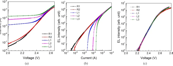
Figure 1 shows the V–I, current–optical power (I–L), and voltage–optical power (V–L) characteristics of five LEDs investigated in this study. Their optical and electrical char-acteristics differ, and the samples can be classified into two groups according to their levels of forward leakage current,
(a) (b) (c)
FIG. 1. Electrical and optical properties of the tested LEDs: (a) Voltage–current (V–I), (b) current–optical power (I–L), and (c) voltage–optical power (V–L) characteristics.
as listed in Table 1. Two LEDs with minimal leakage (R group) and three LEDs with considerable forward leakage (L group) are shown in Fig. 1(a). It is observed that EL ap-pears at different current levels due to the different leakages of the LEDs, as shown in Fig. 1(b). The turn-on voltages (slightly higher than 2.2 V) are similar for the LEDs, ex-cept for those with large leakages, as shown in Fig. 1(c). The PL properties and luminescence images of the LEDs are shown in Fig. 2. Figure 2(a) shows PL intensity under open-circuit conditions (LPLOC) with respect to the excitation laser power. The different leakage properties result in dif-ferent PL properties, especially in the low-excitation range. The open-circuit voltages for the LEDs are in the range of 2.387–2.484 V at 10.9 mW of excitation. The inset shows the luminescence images of LEDs R1 (without electrical leakage) and L3 (with significant leakage) at a 10.9-mW excitation under open-circuit conditions. Another PL mea-surement is performed for each LED under a fixed forward bias of 2.2 V, which is slightly less than the optical turn-on voltage of the LEDs in the R group. This bias condition is selected to prevent the possible generation of EL by recom-bination of photocarriers, because EL can appear during photoexcitation when the open-circuit voltage exceeds the
optical turn-on voltage [15]. Accordingly, Fig. 2(b) shows the PL properties of a limited photoexcited area; there is no significant difference in PL-intensity variation with excita-tion power for the LEDs, except for slightly lower intensi-ties in those with considerable leakage. The descriptions can be supported by the images in the inset, showing the PL images of LEDs R1 and L3 at 10.9 mW excitation under 2.2 V forward bias. Figure 2(c) shows the intensity differences
LPLdiff after subtracting the PL intensity under forward bias of 2.2 V (LPL2.2V) from the LPLOC at the given excitation pow-er. The trend of the intensity change for LPLdiff with respect to excitation power resembles that in the I–L plots shown in Fig. 1(b). Therefore, it is expected that a correlation exists between the PL-intensity difference and EL induced during photoexcitation. Some of the important LED parameters measured during photoexcitation are listed in Table 1.
3.2. Relationship between Photocurrent and EL Extracted from PL
During the photoexcitation process at a fixed forward bias less than the optical turn-on voltage, reverse photocur-rent also exists in addition to PL, as listed in Table 1. When the forward bias is 2.2 V, the reverse photocurrent is around TABLE 1. Measured values of LEDs tested under 10.9-mW photoexcitation
Sample PL intensity under open circuit conditions (L
PLOC) (arb. unit)
Current under forward bias of 2.2 V from V–I plot (Ileak) (A)
Reverse current under bias of 2.2 V (Irev) (A)
Short-circuit current (ISC) (A) R1 1.82 × 10⁵ 3.52 × 10⁻⁷ 3.53 × 10⁻⁴ 7.81 × 10⁻⁴ R2 1.75 × 10⁵ 5.24 × 10⁻⁷ 3.44 × 10⁻⁴ 7.63 × 10⁻⁴ L1 1.60 × 10⁵ 2.30 × 10⁻⁵ 3.24 × 10⁻⁴ 7.58 × 10⁻⁴ L2 1.54 × 10⁵ 8.01 × 10⁻⁵ 2.70 × 10⁻⁴ 7.76 × 10⁻⁴ L3 1.14 × 10⁵ 1.89 × 10⁻⁴ 1.47 × 10⁻⁴ 7.31 × 10⁻⁴ (a) (b) (c)
FIG. 2. PL intensity with respect to excitation power, and PL images, for the tested LEDs: (a) PL intensity under open-circuit conditions (inset: PL images of LEDs R1 and L3 at 10.9 mW excitation under open-circuit conditions), (b) under forward bias of 2.2 V (inset: PL images of LEDs R1 and L3 at 10.9 mW excitation under 2.2 V forward bias), and (c) difference between the two PL intensities.
0.35 mA at 10.9 mW photoexcitation for the LEDs without any significant leakage tested in this study. The photocur-rent increases with excitation power under the fixed bias condition. The measured reverse current Irev is obtained by subtracting the forward leakage current Ileak from the gener-ated photocurrent Iphoto. The relationship between Irev and
Iphoto at a given photoexcitation can be expressed by Eq. (1):
Irev = Iphoto – Ileak. (1) Figure 3 shows the reverse current Irev quantified during the PL measurement under a 2.2-V forward bias. The plot resembles that of LPLdiff shown in Fig. 2(c). The intensity reduction from LPLOC at a bias of 2.2 V may be related to Irev flowing to maintain the constant bias. To compare the lumi-nescence intensities of LEDs, however, Iphoto should be con-sidered as the electrical-excitation level that possibly cor-responds to the photogenerated current, regardless of any amount of leakage. The PL intensities obtained for the 10.9 mW optical excitation are compared to the EL intensities measured for the electrical excitation at 0.35 mA, which is the average Iphoto value for the five LEDs under 10.9 mW excitation power and 2.2 V forward bias. Figure 4 shows the relationship between the three PL-related intensities (i.e.
LPLOC, LPL2.2V, and LPLdiff) and the measured EL intensity for the LEDs at an injection current of 0.35 mA. The measured EL intensity shows an acceptable correlation with LPLdiff, but the correlation with LPLOC is less satisfactory. For each LED,
LPL2.2V is similar and shows no correlation with EL intensity. The LPLdiff values exhibit a directly proportional relationship with EL intensity at a forward current equal to Iphoto under the measurement conditions, and the two intensity values for each LED are practically identical.
Further evidence proving that LPLdiff may be considered as the EL induced by photoexcitation is the luminescence spectrum. Figure 5 shows luminescence spectra under vari-ous conditions for LED R1. The sum of the PL spectrum under 10.9 mW photoexcitation at 2.2 V bias and the EL spectrum for an injection current of 0.35 mA (this amperage equals Iphoto measured under 10.9 mW-excitation at 2.2 V bias) is consistent with the spectrum obtained under open-circuit conditions. This result indicates that the PL under open-circuit conditions contains luminescence contributed
FIG. 3. Reverse current measured during photoexcitation under 2.2 V forward bias.
FIG. 4. Comparison of PL intensities obtained under 10.9 mW excitation power with EL intensities at 0.35 mA for the tested LEDs.
Excitation power
FIG. 5. Consistency of the PL spectrum under open-circuit conditions with the sum of the PL spectrum obtained under 2.2 V bias and the EL spectrum under 0.35 mA injection current.
by the EL process when the open-circuit voltage exceeds the optical turn-on voltage. Moreover, LPLdiff is consider-ably similar to the EL intensity at a forward current equal to
Iphoto, under the given photoexcitation and forward bias. As it is observed that the plot of Irev shown in Fig. 3 re-sembles that of LPLdiff in Fig. 2(c), the relationship between
LPLdiff and Irev is analyzed. The changes in the intensity and current from the maximum intensity and photocur-rent values at a given photoexcitation level, i.e. LPLOC and
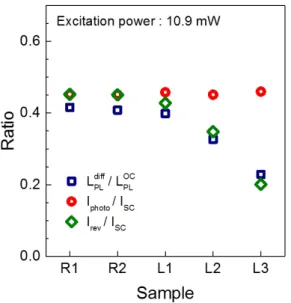
ISC respectively, are compared. The results obtained under 10.9 mW excitation power at 2.2 V forward bias, which are listed in Table 1, are employed for the comparison. In Fig. 6, the ratio of the intensity difference to the maximum PL intensity LPLOC and the ratio of the current to the maximum reverse current ISC are plotted. Ratios of LPLdiff to LPLOC in the range 0.23–0.42 for the LEDs are plotted. The photocurrent
Iphoto that is expected to flow under the test conditions is similar for the LEDs, regardless of the existence of leakage. The ratios of Iphoto to ISC for the tested LEDs are in the range 0.45–0.46. For the LEDs with no leakage, the values of the intensity ratio and photocurrent ratio are close, whereas for the LEDs with electrical leakage, large discrepancies between the two ratios are observed. The foregoing is at-tributed to Ileak, which is the difference between the mea-sured Irev and generated Iphoto, as expressed in Eq. (1). After considering Ileak, the ratio of Irev to ISC follows that of LPLdiff to LPLOC. From the results, the relationship can be expressed using Eq. (2):
������� ����� =
����
���. (2)
The above is similar to the equation used to describe the correlation between electrical leakage and PL-intensity
re-duction [7, 16]. The reasons for this are that the relationship between carrier flow and PL-intensity reduction is similar, and the carrier transport direction is identical. Based on the premise that the PL intensity under short-circuit conditions
LPLSC is negligible, the maximum PL intensity is assumed to be LPLOC. However, because electron-blocking layers in the LED structures can obstruct part of the carrier flow [17], the LPLSC value is occasionally sufficiently large to be in-corporated into the equation, thus affording a more precise comparison. The problem is that the PL cannot be handily derived under short-circuit conditions by most PL measure-ment systems, without any electrical-contact tools. There-fore, LPLOC is employed as the maximum PL intensity for the analyses conducted in this study to evaluate a probeless method.
Figure 7 shows the PL intensity differences LPLdiff with respect to the currents whose values correspond to those of photocurrents under various forward-bias conditions, which are less than 2.2 V, as well as 2.2 V bias for LED R1. The values are compared to the I–L curve, which shows the EL intensity obtained by electrical excitation. The relation-ship between LPLdiff and the current obtained at 2.2 V bias is consistent with the I–L characteristic. Furthermore, the intensity differences obtained even at lower biases do not deviate greatly from the measured EL properties, for LED R1. The results indicate that there is an acceptable forward-bias range for extracting LPLdiff and current levels to estimate the EL intensity, provided that the forward bias suppressing the EL is not considerably lower than the optical turn-on voltage.
3.3. Estimation of EL Intensity
Equation (2) can be rewritten as follows:
FIG. 6. Comparison of ratios of PL-intensity difference to PL intensity under open-circuit conditions and ratios of reverse
������� � �����∙�����
��. (3)
As discussed in the previous sections, LPLdiff can be consid-ered as the EL intensity at a forward injection current equal to Iphoto. Therefore, LPLdiff in Eq. (3) may be replaced by the estimated EL intensity LELe. Hereafter, Eq. (1) is substituted into Equation (3), which can then be rewritten as follows:
����� �����∙ �������� �� −
�����
��� � . (4)
The ratio of the leakage current can be calculated using Eq. (5), in which the PL intensity of the sample with the least leakage among the tested LEDs is LPLOC,max [7]:
ܫ୪ୣୟ୩
ܫୗେ ൌ ͳ െ ቆ ܮେ
ܮେǡ୫ୟ୶ቇ . (5) Then the estimated EL intensity is obtained as follows:
ܮൌ ܮେή ቊܫ୮୦୭୲୭ܫ ୗେ െ ͳ ቆ
ܮେ
ܮେǡ୫ୟ୶ ቇቋ . (6) The ratio of Iphoto to ISC depends on the test conditions for the intensity difference and LED structures. Uniformity is necessary to obtain similar current values at a given ratio, to compare the estimated EL intensities of LED chips at a fixed current value. In this study the aforementioned ratio is 0.455 at 10.9 mW excitation under 2.2 V bias. For more precise calculation of EL intensities, it would be better if the photocurrent ratio or ISC were obtained from PL mea-surements. However, it was shown that ISC can be related to the absorption of the excitation laser in the active layer and
the carrier escape ratio, and other experimental techniques should be employed to analyze the relationship between ISC and the excitation power [18]. Although the actual ISC value is not provided by PL measurements, the comparison of EL intensities among the LED chips on a wafer can be imple-mented within the range of possible current values, which is assumed from the excitation power, because changes in the photocurrent ratio or ISC simply affect the slope and in-tercept of the linear relationship between the estimated and measured values.
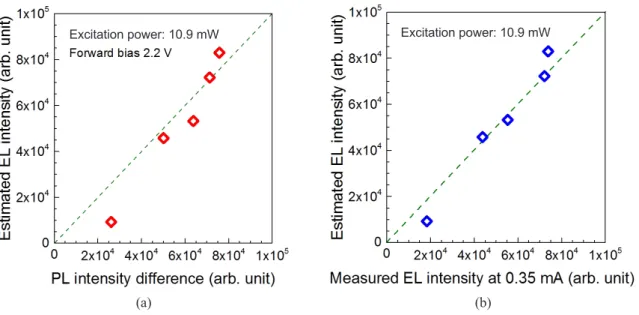
To verify the validity of Eq. (6), the EL intensities es-timated for the five LEDs are compared to the measured EL intensities at 0.35 mA (the average Iphoto under the test conditions). For the estimation, the photocurrent ratio used was 0.455, to cause the current values to approach the value of Iphoto obtained at excitation of 10.9 mW under 2.2 V bias, and LPLOC of LED R1 was incorporated as LPLOC,max. The comparisons between LELe and the measured luminescence intensities are shown in Fig. 8. Figure 8(a) shows LELe with respect to LPLdiff under 10.9 mW photoexcitation and 2.2 V bias, and Fig. 8(b) shows LELe with respect to the measured EL intensity at 0.35 mA. The results exhibit an acceptable linear relationship, indicating that the EL intensities of the LEDs can be estimated and compared using the values ob-tained from PL measurements.
IV. CONCLUSION
The relationship between PL and EL properties was in-vestigated, based on the PL intensity measured under open-circuit conditions and the intensity reduction due to an applied forward bias. It was found that the magnitude of the decrease in PL intensity is consistent with the EL intensity electrically excited by a forward injection current of the
FIG. 8. Comparisons between estimated EL intensities and measured luminescence intensities: (a) Estimated EL intensity with respect to PL-intensity difference under 2.2 V bias, and (b) estimated EL intensity with respect to measured EL intensity.
(a) (b)
same magnitude as the reverse photocurrent under forward bias at photoexcitation. The results can be expressed us-ing an equation showus-ing the relationship between the ratio of the reverse photocurrent to the short-circuit current, the possible maximum photocurrent at the given photoexcita-tion, and the ratio of the PL intensity difference to the pos-sible maximum PL intensity corresponding to the pospos-sible maximum photocurrent. A method for estimating the EL intensity using this relationship is proposed. The results show that the PL measurements may be a reasonable basis for evaluating the EL properties of LEDs that cannot be as-sessed via the contact-probe method.
ACKNOWLEDGMENT
This work was supported by the Research Project of Core Technology for Industry Leading Manufacture (EO-20-0019) of the Korea Institute of Industrial Technology.
REFERENCES
1. E. F. Schubert and J. K. Kim, “Solid-state light sources getting smart,” Science 308, 1274–1278 (2005).
2. M. Anandan, “Progress of LED backlights for LCDs,” J. Soc. Inf. Disp. 16, 287–310 (2008).
3. T. Wu, C.-W. Sher, Y. Lin, C.-F. Lee, S. Liang, Y. Lu, S.-W. H. Chen, W. Guo, H.-C. Kuo, and Z. Chen, “Mini-LED and micro-LED: promising candidates for the next generation dis-play technology,” Appl. Sci. 8, 1557 (2018).
4. C. J. Raymond and Z. Li, “Photoluminescence metrology for LED characterization in high volume manufacturing,” Proc. SPIE 8681, 86810P (2013).
5. A. Yamaguchi, S. Komiya, I. Umebu, O. Wada, and K. Akita, “Photoluminescence intensity in InGaAsP/InP double-hetero-structures,” Jpn. J. Appl. Phys. 21, L297–L299 (1982). 6. Y. H. Aliyu, D. V. Morgan, and H. Thomas, “A luminescence
mapping technique for rapid evaluation of visible-light-emit-ting materials used in semiconductor light-emitvisible-light-emit-ting diodes,” Meas. Sci. Technol. 8, 437–440 (1997).
7. J. Kim, H. Kim, S. Kim, W.-J. Choi, and H. Jung, “Electrical leakage levels estimated from luminescence and photovoltaic properties under photoexcitation for GaN-based light-emitting diodes,” Curr. Opt. Photon. 3, 516–521 (2019).
8. H. Masui, S. Nakamura, and S. P. DenBaars, “Experimental
technique to correlate optical excitation intensities with elec-trical excitation intensities for semiconductor optoelectronic device characterization,” Semicond. Sci. Technol. 23, 085108 (2008).
9. L. Li, P. Li, Y. Wen, J. Wen, and Y. Zhu, “Temperature depen-dences of photoluminescence and electroluminescence spectra in light-emitting diodes,” Appl. Phys. Lett. 94, 261103 (2009). 10. A. Laubsch, M. Sabathil, J. Baur, M. Peter, and B. Hahn,
“High-power and high-efficiency InGaN-based light emitters,” IEEE Trans. Electron Dev. 57, 79–87 (2010).
11. K. Aoyama, A. Suzuki, T. Kitano, S. Kamiyama, T. Takeuchi, M. Iwaya, and I. Akasaki, “Study on efficiency component es-timation of 405 nm light emitting diodes from electrolumines-cence and photolumineselectrolumines-cence intensities,” Jpn. J. Appl. Phys.
52, 08JL16 (2013).
12. G.-B. Lin, E. F. Schubert, J. Cho, J. H. Park, and J. K. Kim, “Onset of the efficiency droop in GaInN quantum well light-emitting diodes under photoluminescence and electrolumines-cence excitation,” ACS Photon. 2, 1013–1018 (2015).
13. W.-A. Quitsch, D. Sager, M. Loewenich, T. Meyer, B. Hahn, and G. Bacher, “Low injection losses in InGaN/GaN LEDs: the correlation of photoluminescence, electroluminescence, and photocurrent measurements,” J. Appl. Phys. 123, 214502 (2018).
14. J. Kim, S. Kim, H. Kim, W.-J. Choi, and H. Jung, “Effects of carrier leakage on photoluminescence properties of GaN-based light-emitting diodes at room temperature,” Curr. Opt. Photon. 3, 164–171 (2019).
15. M. F. Schubert, Q. Dai, J. Xu, J. K. Kim, and E. F. Schubert, “Electroluminescence induced by photoluminescence excita-tion in GaInN/GaN light-emitting diodes,” Appl. Phys. Lett.
95, 191105 (2009).
16. Y. Augarten, T. Trupke, M. Lenio, J. Bauer, J.W. Weber, M. Juhl, M. Kasemann, and O. Breitenstein, “Calculation of quan-titative shunt values using photoluminescence imaging,” Prog. Photovoltaics 21, 933–941 (2013).
17. A. David and N. F. Gardner, “Droop in III-nitrides: compari-son of bulk and injection contributions,” Appl. Phys. Lett. 97, 193508 (2010).
18. J.-H. Song, H.-J. Kim, B.-J. Ahn, Y. Dong, S. Hong, J.-H. Song, Y. Moon, H.-K. Yuh, S.-C. Choi, and S. Shee, “Role of photovoltaic effects on characterizing emission properties of InGaN/GaN light emitting diodes,” Appl. Phys. Lett. 95, 263503 (2009).