1. INTRODUCTION
Operational amplifiers are the basic building blocks in both analog and mixed-signal circuits. The operational amplifiers used in hearing aids are specially designed to meet the requirements of low voltage, single-supply, low power dissipation, high gain, etc. Because the input signal from microphone is very small, less than 1mV, the op-amp is designed to be very sensitive to such a tiny signal. On the other hand, the op-amp should have a rail-to-rain output swing as well as a very low output impedance to avoid distortion and waste of power.
Fig. 1 The Application Schematic
2. OPERATIONAL AMPLIFIER
The op-amp consists of three stage, input stage, gain stage and output stage. The input stage is an N-channel differential pair. The gain stage is a current load common source P-channel transistor. A class AB push pull stage acted as the output buffer to deal with a small resistor load.
Fig. 2 Top level op-amp structure
2.1 Input Stage
The input signal is less than 0.01mV. That is,
mV V V mV Vc-0.01 < c< c+0.01 (1) TN DSAT DSAT in
V
V
V
V
³
5+
1+
(2) TN DSAT DD inV
V
V
V
£
-
4-
(3)Where
V
DSAT5V
DSAT4andV
DSAT1are the saturation
voltage of transistors M5, M4 and M1.
V
TNis the
threshold voltage of N channel transistor.
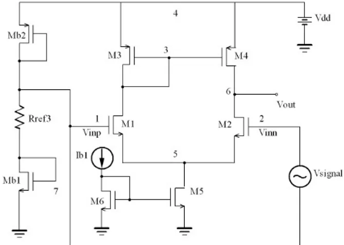
So in the design, we do not need to take cascode in input stage to extend the common mode input range (ICMR). A regular N-channel differential pair input stage provides enough ICMR for the op-amp. We chose a carrier, Vc = 0.7V. Fig 2 shows the transistor level schematic. Transistors Mb1, Mb2 and the resistor Rref compose a voltage divider to provide the carrier for the circuit. Node 6 is the output to the next stage. Vsignal is the input signal.Fig. 3 Transistor Level Schematic of Input Stage
)
//
(
2
2
1 o D m id od dmV
g
R
r
V
A
=
=
-
(4)
Equation. (4) state the relationship among circuit parameters, where
V
odis the differential mode output
voltage and
V
idis the differential mode input voltage.
m
g
is the transconductance of transistor M2, M1.
R
Dis the
equivalent load resistance. To improve the gain, weA CMOS Single-Supply Op-Amp Design For Hearing Aid Application
Soon-Suck Jarng*, Lingfen Chen
**, You-Jung Kwon
** Department of Information Control & Instrumentation, Chosun University, Gwang-Ju, Korea (Tel : +82-62-230-7107; E-mail: ssjarng@chosun.ac.kr)
Abstract: The hearing aids specific operational amplifier described in this paper is a single-supply, low voltage CMOS amplifier.
It works on 1.3V single-supply and gets a gain of 82dB. The 0.18μm CMOS process was chosen to reduce the driven voltage as well as the power dissipation.
may increase the gate length of the M1 and M2, the ratio of W/L or reduce the current from current source Ib1.
Fig. 4 (a) AC Output Wave of Input Stage.
Fig. 4 (b) DC Output Wave of Input Stage. Table 1 The scale of transistors.
Transistor W [μm] L [μm] M1 16.30 1.00 M2 16.30 1.00 M3 23.74 1.00 M4 23.74 1.00 M5 10.63 1.00 M6 10.63 1.00 M7 10.21 1.00
Table 2 small-signal transfer characteristics
Vout/Vin 115.97
Input Resistance 1.000e+20 Output Resistance 565.317k
2.2 Gain Stage
The gain stage used in the design is a regular active load common source amplifier. M11, M10, Rref2 and M9 compose a current source. The diode connection transistor M11 could be regarded as a large resister so that we can reduce the size of the resistor, Rref. M10 is exactly the same as M9 so that the current through M11 equals to the current through the transistor M8. Vinput is the output from input stage. The hearing aids are only interested in the low frequency input signals which covers between 20 Hz and 8kHz. We found there is no phase shift when the input frequency is less then 10E4 Hz even we did not do any frequency compensation. Fig. 5 shows the structure of the gain stage.
The gain of active load common source transistor is determined by the transconductance of the transistor M8 and the equivalent load resistance. Equation. (4). So we can increase the gate length, the W/L to get a larger gain. Reduce current also help to do so. Fig. 6 show the frequency response of the gain stage.
Table 2 shows the small signal transfer characteristics of the gain stage. It got a gain of 92.78 at low frequency. Table 2 small-signal transfer characteristics
Vout/Vin 92.78
Input Resistance 1.000e+20 Output Resistance 466.102k
Fig. 5 Transistor Level Schematic of Gain stage
100 102 104 106 108 17 17.5 18 18.5 19 19.5 Freq/[Hz] A mpl itu d e/[ V]
Fig. 6 (a) Amplitude-Frequency Response
101 102 103 104 105 106 107 140 145 150 155 160 165 170 175 180 Freq/[Hz] P ha /[R a d/S e c]
Fig. 6 (b) Phase-Frequency Response
2.3 Output Stage
less than 0.01mV. The output is
mV
V
V
mV
V
oc-
100
£
OUT£
oc+
100
So a source follower was chosen to be the output stage. (Fig. 7)
Fig. 7 Transistor Level Schematic of Output Stage
Fig. 8 (a) DC Transfer Characteristic
Fig. 8 (a) AC Transfer Characteristic Table 3 Small-Signal Transfer Characteristics
Vout/Vin 978.2m Input Resistance 1.000e+20 Output Resistance 28.23k
3. FULL CIRCUIT SIMULATION AND TEST
Fig. 9 shows the full schematic of the op-amp. In this schematic, the voltage divider which produce the carrier was not included. The transistors M7, M6, M5 and resistor Rref compose a current source. M1, M2, M3, M4 and M5 consist a N-Channel differential pair. M5 provided a tail current. The transistor M8 is a common source amplifier with a current
source load. The transistor M10 is a source follower. All these parts are analyzed and simulated on former section. Here we tested the specifications of the op-amp.
The specifications we interested in are gain, phase margin, ICMR, Common Mode Reject rang (PRSS), output swing, Common Mode Rejection Range (CMRR) and Settling time.
Fig. 9 The Full Schematic of the Op-amp
3.1 Frequency response
Table 4 and Fig. 10 show frequency response of op-amp. The gain is 82dB. There is enough phase margin to deal with low frequency with acceptable phase shift.
Table 4 Small-Signal Transfer Characteristics Vout/Vin 12.25k Input Resistance 1.000e+20 Output Resistance 25.04k 102 104 106 108 0 10 20 30 40 50 60 70 80 90 Freq/[Hz] A mpl itu d e/[d B]
102 103 104 105 106 107 108 -200 -150 -100 -50 0 50 100 150 200 Freq/[Hz] P h a/[D gr e e]
Fig. 10 (b) Phase-Frequency Response
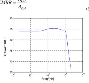
3.2 CMRR
CMRR, Common Mode Reject Range, is defined as Equation. (5). The Acm is common-mode gain and the A dm is the differential-mode gain. In fig. 11(a), we use th e absolute value. DM CM
A
A
CMRR
=
(5)
102 104 106 108 1010 65 70 75 80 85 90 Freq/[Hz] |C M R R|/[ d B]
Fig. 11 (a) CMRR Amplitude-Frequency Response
102 104 106 108 1010 -120 -100 -80 -60 -40 -20 0 Freq/[Hz] Arg [C M R R](d gr e e)
Fig11 (b) CMRR Phase-Frequency Response
3.3 Output Swing
The output is between 0V and 767mV when the input varies in the ICMR.
Fig. 12 Output Swing.
3.4 PSRR
PSRR, Power-Supply Rejection Ratio. Assume that the chip ground is reliable. The test only on the supply. It turned out to be 125dB at 0dB. 102 104 106 108 20 40 60 80 100 120 140 Freq/[Hz] A mpl itu d e/[V ]
Fig. 13 PSRR Amplitude Frequency Response
3.5 Settling Time
We added a tiny pulse on input. The Settling time is: Settling Time+ = 31ns;
Settling Time- = 73ns.
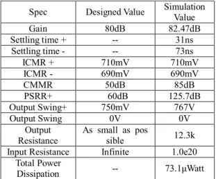
Table 5 Specifications.
Spec Designed Value Simulation Value
Gain 80dB 82.47dB Settling time + -- 31ns Settling time - -- 73ns ICMR + 710mV 710mV ICMR - 690mV 690mV CMMR 50dB 85dB PSRR+ >60dB 125.7dB Output Swing+ 750mV 767V Output Swing_ 0V 0V Output
Resistance As small as possible 12.3k Input Resistance Infinite 1.0e20
Total Power
Dissipation -- 73.1μWatt
4. CONLUSION
A low voltage single-supply operational amplifier for hearing aids application was designed in this paper. By using short channel devices, it works on a 1.3V single supply and get a gain of 82dB. The analog circuit involved in hearing aids design contributes a lot to the high performance of the chip. We will further our research on this area.
ACKNOWLEDGMENTS
This study was supported by research fund from the ministry of commerce, industry and energy (MOCIE Korea) standardization technology development project(standardization study on digital hearing aid: project number 10016821) in 2004.
REFERENCES
[1] Phillip E. Allen, Douglas R. Holberg, “CMOS Analo g Circuit Design”, Second Edition.
[2] David A Johns, Ken Martin, “Analog Integrated Circ uit Design”.
[3] Paul R. Gray, Paul J. Hurst, Stephen H. Lewis, Rob ert G. Meyer, “Analysis And Design of Analog Inte grated Circuits, Fourth Edition”.
Appendix I.
HSPICE CODING
1) Differential Pair
****N channel differential pair***** .lib '/usr/COMLIB/L18.lib’ nn .option post = 2 vdd 4 0 1.3 vinn 1 0 sin(.7 .01m 1000 0 0 ) vinp 2 0 .7 rref 7 8 10k m1 3 1 5 5 nch w = 16u l = 1u as = 21.76f ad = 21.7 6f ps = 18.72u pd = 18.72u m2 6 2 5 5 nch w = 16u l = 1u as = 21.76f ad = 21.7 6f ps = 18.72u pd = 18.72u m3 3 3 4 4 pch w = 23.70u l = 1u as = 32.23f ad = 3 2.23f ps = 26.42u pd = 26.42u m4 6 3 4 4 pch w = 23.70u l = 1u as = 32.23f ad = 3 2.23f ps = 26.42u pd = 26.42u m5 5 7 0 0 nch w = 10.63u l = 1u as = 14.46f ad = 1 4.46f ps = 13.35u pd = 13.35u m6 7 7 0 0 nch w = 10.63u l = 1u as = 12.54f ad = 1 2.54f ps = 12.99u pd = 12.99u m7 8 8 4 4 pch w = 10.87u l = 1u as = 14.78f ad = 1 4.78f ps = 13.59u pd = 13.59u .op .tf v(6) vinn .tran .01m 5m .print tran v(6) .end 2) Gain Stage *********** Gain stage ********************** .lib '/usr/COMLIB/ L18.lib’ nn
.option post = 2 vdd 4 0 1.3 ib 10 0 25u vin 1 0 sin( .75 .1m 1000 0 0) .para lm = 1u M1 9 10 4 4 pch w = 46.78u l = lm as = 55.2f ad = 55.2f ps = 49.14u pd = 49.14u M2 9 1 0 0 nch w =10.91u l = lm as = 12.9f ad = 12. 9f ps = 13.27u pd = 13.27u M3 10 10 4 4 pch w = 13.56u l = lm as =18.1f ad = 18.1f ps = 15.92u pd = 15.92u .op .tf v(9) vin .tran .01m 5m .print tran v(9) .end 3) Output Stage
**** N-channel Source Follower with Bias.**** .lib '/usr/COMLIB/L18.lib’ nn
.option post = 2 vdd 4 0 1.3
vin 1 0 sin(.9 .1 1000 0 0) * Input signal * vin 1 0 dc = .7
m1 4 1 2 2 nch w= .42u l = .18u as = 0.15f ad = 0.1 5f ps = 1.14u pd = 1.14u
m2 2 3 0 0 nch w= .22u l = .18u as = 0.08f ad = 0.0 8f ps = 0.58u pd = 0.58u m3 3 3 0 0 nch w= .22u l = .18u as = 0.08f ad = 0.0 8f ps = 0.58u pd = 0.58 m4 5 5 3 3 nch w= .22u l = .18u as = 0.08f ad = 0.0 8f ps = 0.58u pd = 0.58 rref 4 5 10k rload 2 0 8k
.tf v(2) vin * Small signal a nalysis .op .tran .01m 5m .print tran v(2) * .dc vin 0 2 .1 * .print dc v(2) .end
4) Full Operational Amplifier
*** The Full operational amplifier ************ .lib '/usr/COMLIB/L18.lib’ nn .option post = 2 vdd 4 0 1.3 *vinn 1 0 sin(.7 .01m 1000 0 0 ) vinn 2 0 dc = .7 ac = 0.01m vinp 1 0 .7 rref1 7 8 10k rref2 4 11 80k m1 3 1 5 5 nch w = 16.00u l = 1u as = 21.76f ad = 2 1.76f ps = 18.72u pd = 18.72u m2 6 2 5 5 nch w = 16.00u l = 1u as = 21.76f ad = 2 1.76f ps = 18.72u pd = 18.72u m3 3 3 4 4 pch w = 23.70u l = 1u as = 32.23f ad = 3 2.23f ps = 26.42u pd = 26.42u m4 6 3 4 4 pch w = 23.70u l = 1u as = 32.23f ad = 3 2.23f ps = 26.42u pd = 26.42u m5 5 7 0 0 nch w = 10.63u l = 1u as = 14.46f ad = 1 4.46f ps = 13.35u pd = 13.35u m6 7 7 0 0 nch w = 10.63u l = 1u as = 14.46f ad = 1 4.46f ps = 13.35u pd = 13.35u m7 8 8 4 4 pch w = 10.87u l = 1u as = 14.78f ad = 1 4.78f ps = 13.59u pd = 13.59u m8 9 6 4 4 pch w = 47.31u l = 1u as = 55.2f ad = 55. 2f ps = 49.14u pd = 49.14u m9 9 7 0 0 nch w = 10.63u l = 1u as =12.9f ad = 12. 9f ps = 13.27u pd = 13.27u m10 4 9 10 10 nch w= .42u l = .18u as =0.15f ad = 0.15f ps = 1.14u pd = 1.14u m11 10 12 0 0 nch w= .22u l = .18u as =0.08f ad = 0.08f ps = 0.58u pd = 0.58u m12 11 11 12 12 nch w= .22u l = .18u as = 0.08f ad = 0.08f ps = 0.58u pd = 0.58u m13 12 12 0 0 nch w= .22u l = .18u as =0.08f ad = 0.08f ps = 0.58u pd = 0.58u .op .tf v(10) vinn .tran .01m 5m .print tran v(10) *.ac dec 100 0 100x *.print ac vdb(10, 2) vp(10) .meas tran p_sup avg power .end