28-2 / J.-H. Lee
• IMID 2009 DIGEST *†‡
* Corresponding author. e-mail : [email protected]
† Current address: Dept. of Chemistry, Imperial College-London, South Kensington Campus, London, U. K.
Abstract
We investigated the doping effects of ReO3 in different
p-type organic semiconductors on the formation of charge transfer complexes and the electrical conductivity by comparing the absorption in ultraviolet-visible-near-infrared (UV-Vis-NIR) and the current density-voltage characteristics of the hole only devices, respectively. The large energy difference between the HOMO level of host and Fermi energy level of dopant (∆E=EHOHO,host -
EF,dopant) gives higher concentration of CT complexes and
enhanced conductivity.
1. Introduction
Electrical doping in organic semiconductors could reduce the contact resistance between the electrodes and organic layers and enhance electrical conductivity. Recently, various combinations of dopants and p-type semiconductors have been reported up to now, including organic dopant such as tetrafluoro-tetracyano-quinodimethane (F4-TCNQ) in 4, 4', 4"-tris(N,N-diphenyl-amino)triphenylamine (TDATA) [1], metal halides such as antimony pentachloride (SbCl5) in N,N'-diphenyl-N,N'-bis(3-methylphenyl)-1,1'-biphenyl-4,4'-diamine (TPD) [2], ferric chloride (FeCl3) [3] and copper iodide (CuI) in 1,4-bis[N-(1-naphthyl)-N'-phenylamino]-4,4' diamine (NPB) [4], and metal oxides such as tungsten oxide (WO3) in
4,4’,4”-tris(N-(2-naphthyl)-N-phenyl-amino)-triphenylamine (2TNATA) [5], vanadium oxide (V2O5) [6], molybdenum oxide (MoO3) [7,8] and rhenium oxide (ReO3) [9] in NPB. These papers demonstrated that the p-dopants form CT complexes with hole transporting organic materials by electron transfer from the organic molecules to the dopants
[1-9]. However, there are few reports about the host dependence on the formation of CT complexes and electrical properties of metal oxide doped organic semiconductors [10].
In previous experiments, we found that the effectiveness of p-dopants in the formation of CT complexes is proportional to the energy difference between the HOMO level of organic materials and the Fermi energy level of p-dopants (∆E=EHOHO,host - EF,dopant) by doping different dopants in a host. Among the dopants of ReO3, MoO3 and CuI possessing different work functions [ReO3 (6.0 eV)>MoO3 (5.7 eV)>CuI (5.4 eV)], ReO3 was the most effective p-dopant with the 2TNATA host [11].
In this presentation, we will report the effectiveness of doping of a p-dopant in different organic semiconductors and will demonstrate that a host possessing high HOMO level results in high concentration of CT complexes at same doping concentrations of ReO3. However, the conductivity does not follow the sequence of concentration of CT complexes. This behavior was interpreted based on the carrier density of doped films and the hole mobility of organic hosts.
2. Experimental
The rhenium oxides (ReO3) (Aldrich) was used as the p-dopant and three different organic semiconductors have been selected as the hosts; 2TNATA, NPB and 1,1–Bis-(4–methylphenyl)-aminophenyl-cyclohexane (TAPC). The ReO3 doped organic layers were formed by coevaporation of the dopant and the host by thermal evaporation under high vacuum. Glass substrates with 150 nm thick patterned
Host effects on electrical conductivity of ReO
3doped organic
semiconductors
Jae-Hyun Lee, Dong-Seok Leem
†and Jang-Joo Kim*
Dept. of Materials Science and Engineering, and Center for OLED
Seoul Nat'l Univ., Seoul, KOREA
TEL: 82-2-875-2412, e-mail: [email protected]
28-2 / J.-H. Lee
IMID 2009 DIGEST • indium tin oxide (ITO) were used to fabricate devices
after cleaning with acetone and isopropyl alcohol. To fabricate the hole only devices, LiF (50 nm), doped organic semiconductor (50 nm) and Ag electrode (50 nm) were successively deposited on ITO electrode. The devices were encapsulated with a getter in the dry nitrogen glove box prior to the measurement of the current density–voltage (J-V) characteristics by a Keithley 2400 semiconductor parameter analyzer. 50 nm thick doped organic films evaporated on glass substrates were used for the ultraviolet-visible-near infrared (UV-Vis-NIR) absorption measurements (Varian, Cary 5000).
3. Results and discussion
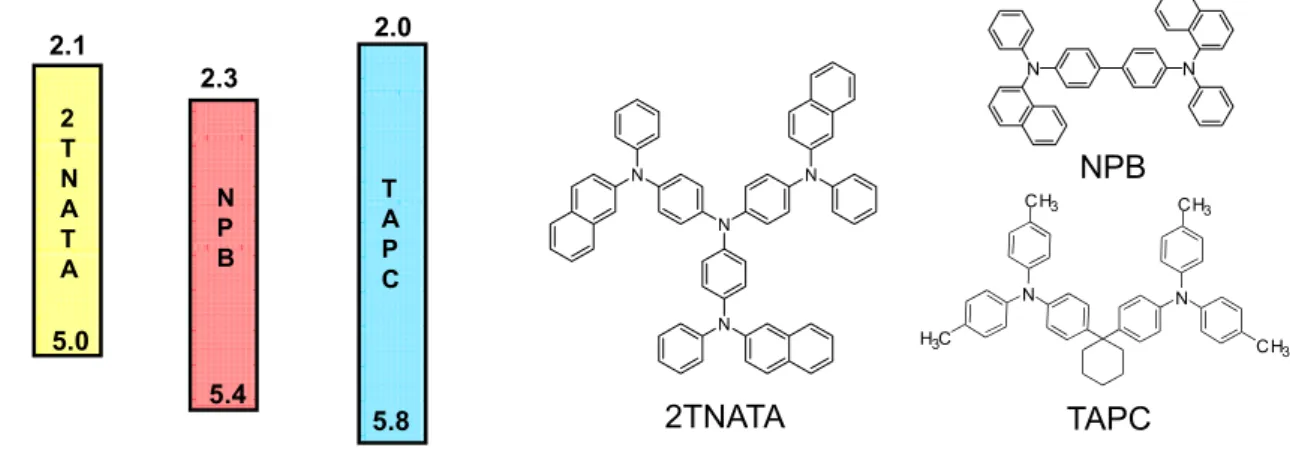
Figure 1 shows the energy level and the molecular structure of the organic semiconductors and the p-type dopant of ReO3. From references and measured data by cyclic voltammetry in our laboratory, we confirmed HOMO level of 5.0 eV for 2TNATA, 5.4 eV for NPB and 5.8 eV for TAPC, respectively. Based on the assumption that the Fermi level of a metal oxide dopant is same as that of bulk semiconductor [12], ReO3 are expected to form the CT complex with the hosts having lower HOMO level than the work functions of ReO3.
Figure 2 shows the UV-Vis-NIR absorbance spectra of 25 mol% ReO3 doped host films and undoped films. The additional absorption peaks in visible and near-infrared regions which are not shown by either component imply the formation of CT complexes. The absorbance spectra of the undoped films show only absorption by π- π* transition near the wavelength of 400 nm and background absorption including the scattering and optical interference of solid film on a
glass substrate. In contrast, the additional peaks of doped host films are located at 434 and 1240 nm for 2TNATA, 490 and 1342 nm for NPB and 450 and 692 nm for TAPC, respectively. These peaks were are originated from the characteristic absorption peaks of the charge transfer complex or the radical cation host molecule (Host+) formed by doping. Intensity of the CT peak becomes smaller as the HOMO level of the hosts getting higher. In other words, larger energy difference between the HOMO level of an organic host and the Fermi level of a p-dopant (∆E=EHOMO,host − EF,dopant) facilitates the formation of CT complexes at the same doping concentration. These results are consistent with previous results of the energy difference of ∆E by using different p-dopants having different Fermi levels in a host [11].
The current density-voltage (J-V) characteristics of ReO3 25 mol% doped 2TNATA, NPB and TAPC are Figure 1. Energy level of 2TNATA, NPB and TAPC, respectively. (b) Molecular structures of organic host materials. N N N N 2TNATA N N NPB TAPC N N CH3 CH3 H3C CH3 2.3 N P B 5.4 2.0 T A P C 5.8 2.1 5.0 2 T N A T A ReO3 : 6.0
Figure 2. The UV-Vis-NIR absorbance spectra of 25 mol% ReO3 doped 2TNATA, NPB and
TAPC films. Inset: absorption spectra of undoped films.
400 800 1200 1600 2000
0.0 0.2 0.4
0.6 ReO3 25 mol% doped
888888888 2TNATA 888888888 NPB 888888888 TAPC A b sor b anc e Wavelength (nm) 400 800 1200 1600 2000 0.0 0.2 0.4 0.6 A b so rb an ce Wavelength (nm)
28-2 / J.-H. Lee
• IMID 2009 DIGEST
summarized in figure 3 obtained from the hole only devices consisting of ITO / ReO3 doped host (50) / Ag (50). ReO3 doped NPB device showed the highest current density at whole voltage range. The conductivity of the 25 mol% ReO3 doped NPB film was measured to be 1.0x10⁻⁶ S/cm at quasi Ohmic region of low voltage range. This enhanced conductivity from undoped film (5.8x10⁻⁸ S/cm) can be interpreted by increased carrier density. In previous results, we demonstrated that the conductivity of a doped host (2TNATA) is enhanced according to the generated free carrier density which was correlated with the concentration of CT complexes [11]. However, the conductivity of three different hosts does not follow the sequence of concentration of CT complexes. Although the ReO3 doped 2TNATA film have higher concentration of CT complexes, the conductivity of ReO3 doped 2TNATA was lower than ReO3 doped NPB. The different sequence could be interpreted by the lower hole mobility of 2TNATA. The hole mobility of undoped host films measured by the time-of-flight (TOF) method are shown in figure 4. The mobility of 2TNATA (3x10⁻⁵ cm2/Vs) is 1~2 order lower than other hosts of NPB (8x10⁻⁴ cm2/Vs) and TAPC (5x10⁻³ cm2/Vs). Since the conductivity is consisted with the carrier density and mobility, the ReO3 doped 2TNATA film had lower conductivity of 1.7x10⁻⁷ S/cm than the ReO
3 doped NPB film.
4. Summary
We investigated the doping effect of ReO3 in different p-type semiconductors such as 2TNATA,
NPB and TAPC possessing different HOMO energy level [TAPC (5.8 eV)>NPB (5.4 eV)>2TNATA (5.0 eV)]. Through the UV-Vis-NIR spectroscopic measurements and the J-V characteristics of hole only device, we demonstrated that higher concentration of CT complexes and carrier densities are generated in the host possessing larger energy difference (∆E=EHOHO,host - EF,dopant). The conductivity of 1.0x10⁻⁶ S/cm was measured from 25 mol% ReO3 doped NPB which has higher mobility than 2TNATA host and larger carrier density than doped TAPC.
Acknowledgement
This research was supported by a grant(2009K000069) from Center for Nanoscale Mechatronics & Manufacturing, one of the 21st Century Frontier Research Programs, which are supported by Ministry of Education, Science and Technology of Korea and the World Class University (WCU) program.
5. References
[1] X. Zhou, M. Pfeiffer, J. Blochwitz, A. Werner, A. Nollau, T. Fritz, and K. Leo, Appl. Phys. Lett. 78, 410 (2001).
[2] C. Ganzorig and M. Fujihira, Appl. Phys. Lett. 77, 4211 (2000).
[3] J. Endo, T. Matsumoto and J. Kido, Jpn. J. Appl. Phys. Part 2 41 (L358) (2002).
[4] J.-H. Lee, D.-S. Leem, and J.-J. Kim, Org. Figure 3. The J-V characteristics of the hole
only device with ReO3 25 mol% doped
2TNATA (rectangle), NPB (circle) and TAPC (triangle).
0.1
1
10
010
110
210
3Current density (mA/cm
2
)
Voltage (V)
ReO3 25 mol% doped
2TNATA NPB TAPC
Figure 4. The hole mobility of undoped 2TNATA (rectangle), NPB (circle) and TAPC (triangle).
0.0
0.2
0.4
0.6
0.8
1.0
10
-510
-410
-310
-2 2-TNATA(h+) NPB(h+) TAPC(h+)E
1/2(MV/cm)
1/2Mo
bility
(cm
2/ Vsec
)28-2 / J.-H. Lee
IMID 2009 DIGEST • Electron. 9, 805 (2008).
[5] C.-C. Chang, M.-T. Hsieh, J.-F. Chen, S.-W. Hwang, and C. H. Chen, Appl. Phys. Lett. 89, 253504 (2006).
[6] X. L. Zhu, J. X. Sun, H. J. Peng, Z. G. Meng, M. Wong, and H. S. Kwok, Appl. Phys. Lett. 87, 153508 (2005)
[7] H. Ikeda, J. Sakata, M. Hayakawa, T. Aoyama, T. Kawakami, K. Kamata, Y. Iwaki, S. Seo, Y. Noda, R. Nomura, and S. Yamazaki, SID Int. Symp. Digest of Tech. Papers, 37, 923 (2006)
[8] T. Matsushima and C. Adachi, J. Appl. Phys. 103, 034501 (2008).
[9] D.-S. Leem, H.-D. Park, J.-W. Kang, J.-H. Lee, J. Kim, and J.-J. Kim, Appl. Phys. Lett. 91, 011113 (2007).
[10] K-H. Yim, G. L. Whiting, C. E. Murphy, J. J. M. Halls, J. H. Burroughtes, R. H. Friend and J.-S. Kim, Adv. Mater. 20, 3319 (2008)
[11] J.-H. Lee, D.-S. Leem, H.-J. Kim and J.-J. Kim, Appl. Phys. Lett. 94, 123306 (2009).
[12] Q. Sun, B. K. Rao, P. Jena, D. Stolcic, Y. D. Kim, G. Gantefor, and A. W. Castleman, Jr., J. Chem. Phys., 121, 9417 (2004).