Solid State Thick Film X-ray Image Sensor
Yun Yi1, Sun Woo Yuk1, Shin Woong Park1, Sun Ung Kim2, Ki Hyun Kim3
1 Dept. of Electronics & Information Engineering, Korea University. 2 Dept. of Semiconductor and Display Physics, Korea University.
3 Samil Pharmaceutical Cooperation
E-mail : [email protected] 1. Introduction
There are various technologies in detecting X-ray which was discovered more than 100 years ago. While screen-film system was the traditional method of detecting X-ray, direct or indirect detection of X-ray is relatively recent development. Since the X-ray accompanies an ionization process, it is desired to be exposed less. The more efficient radiation detector used in detecting X-ray, the less probable to be exposed to such radiation. There are many efficient X-ray detecting material are known such as PbI2, HgI2, CdTe, which are wide gap semiconductors. CdZnTe is one of them, which has high atomic number so that it has larger scattering cross section when atoms are scattered by X-ray. These single crystals are not easy to grow and difficult to handle, particularly in large area detection application. For the large area detection application, we have chosen poly-crystalline thick film as X-ray conversion material which has high atomic number and can be grown in large area. Though the physical characteristics and electrical properties may not be as good as those of single crystal, poly-crystalline thick film CdZnTe is very attractive material for large area or linear array detector application.
2. Methods and Results
2.1 Detector
High zinc composition CdZnTe compounds have low leakage current due to wide energy gap, but have poor charge collection efficiency due to low electron mobility. In this experiment we synthesized CdZnTe :Cl (Zn = 4%) polycrystalline materials. Then the CdZnTe thick films are deposited on ITO coated glass below 500°C by thermal evaporation. In order to measure the electrical properties of the CdZnTe thick films, gold electrode was prepared by thermal evaporation method with thickness of 1000Å. It had shown a good Ohmic contact in the figure 1.
Room temperature current-voltage measurements were carried out using an electro-meter (Keithley 2010) and a dc high-voltage power supply (Keithley 2410) by four probe method.
The average grain size is about 5µm. The grain size was estimated from the Scherrer’s formula given by d = (kλ/βcosθ), where λ = 1.5443Å is the wavelength of the CuK2 line, β is the full width at half maximum of main
peak, and is Scherrer’s constant which approximately equals 1.15 for the (111) orientation in the cubic system[3].
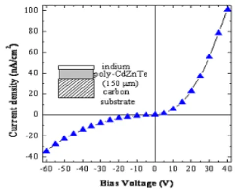
Fig. 1 Current-Voltage character of Au top electrode
The I-V curve of this Schottky contact sample is shown in figure 2. This shows that the Schottky contact function as blocking layer.
Fig. 2 The I-V characteristic of Schottky contact
Moreover, deposited CdZnTe thick films were characterized by XRD in order to analyze their structure. The XRD spectrum of this sample is shown in figure 3.
Fig. 3 XRD Spectrum of Cd1-xZnxTe(x=0.04)
Transactions of the Korean Nuclear Society Autumn Meeting Busan, Korea, October 27-28, 2005
2.2. Data Acquisition System (DAS)
The developed system is composed of a 16 channel linear array Poly-CdZnTe, a dual integrator, and A/D converter, a digital logic interface, and a user interface as shown in figure 4. [4]
Fig. 4 Block diagram of data acquisition system (DAS)
2.3. Experiments
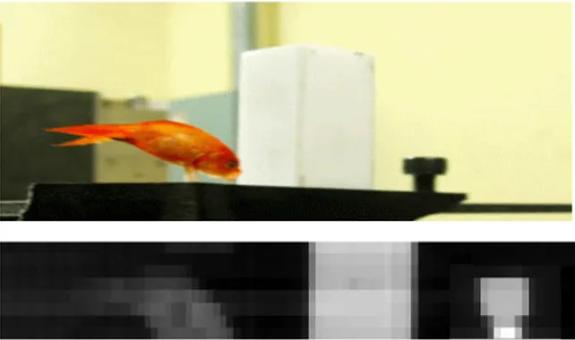
A continuous operating, scanning X-ray source was used for acquiring X-ray image using poly-CdZnTe in this experiment. The test image was acquired as in figure 5 with X-ray system. The Styrofoam and bolt pattern were shown clearly while goldfish pattern was vague. The imaging condition is the tube voltage of 150kVp, tube current of 1mA, and X-ray pulse time of 8.3ms, source to detector distance of 26cm.
Fig 5. X-ray image acquired by poly-CZT
2.4. Results
We have prepared a thick film Cd1-xZnxTe(x=0.04) by thermal evaporation method. The resistivity of the CZT is about 1.2×10¹⁰Ω⋅cm and its thickness is about
150
µ
m . The mobility-lifetime product of poly-crystalline CdZnTe sample is in the range of 8.7×10⁻⁷∼ 5.6×10⁻⁶cm /2 V . For the blocking layer, Schottky
barriers were formed by indium. Moreover, we have built a multi channel data acquisition system (DAS) for many applications and tested under X-ray condition with three phantoms. The Styrofoam and bolt pattern were shown clearly while goldfish pattern was vague.
The phantom image was acquired by the preliminary x-ray test using this DAS. It has shown promising results which can be used as a linear and area detectors.
3. Conclusion
X-ray detector was fabricated with high resistive poly-crystalline CdZnTe and Schottky contact. A linear array type of detector was assembled with data acquisition system and imaged the test objects with X-ray system successfully. We have shown a high resistive polycrystalline CZT can be a good X-ray detector.
The CZT thick film prepared by thermal evaporation method can be pixelized in various ways such as in linear or in area, and also has high quantum efficiency. Therefore, we expect further utilization as a X-ray detector in industry as well as in medicine, particularly as a intra-oral sensor, a panoramic sensor and mammography sensor.
References
[1] K.H. Kim, “Characterization of high resistivity poly CdZnTe thick films grown by thermal evaporation method”, IEEE RTSD, 2004
[2] Satoshi Tokuda, “Preparation and characterization of polycrystalline CdZnTe films for large-area, high-sensitivity X-ray detectors”, J. of Materials Science, Materials in Electronics 15 (2004) 1-8
[3] B.D.Cullity, Elements of X-ray diffraction, 2nd ed.
Reading, MA :Addison-Wesley, 1978, pp.102.
[4] YunYi, “Development of a high SNR data acquisition system for 16 channel X-ray detector module”, EMBC2001