784
-Single Shot White Light Interference Microscopy for 3D Surface Profilometry
Using Single Chip Color Camera
Vishal Srivastava1*, Mohammad Inam2, Ranjeet Kumar3, and Dalip Singh Mehta4
11EIED, Thapar University, Bhadson Road, Patiala, Punjab 147004, India
2Department of Physics, Zakir Husain Delhi College, Opp to RamLeela Ground, Jawaharlal Nehru Marg,
New Delhi, Delhi 110002, India
3Department of Physics, Hindu College, University of Delhi, University Enclave, Delhi, 110007, India 4Indian Institute of Technology Delhi, Hauz-Khas, New Delhi 110016, India
(Received June 30, 2016 : revised October 20, 2016 : accepted November 10, 2016)
We present a single shot low coherence white light Hilbert phase microscopy (WL-HPM) for quantitative phase imaging of Si opto-electronic devices, i.e., Si integrated circuits (Si-ICs) and Si solar cells. White light interferograms were recorded by a color CCD camera and the interferogram is decomposed into the three colors red, green and blue. Spatial carrier frequency of the WL interferogram was increased sufficiently by means of introducing a tilt in the interferometer. Hilbert transform fringe analysis was used to reconstruct the phase map for red, green and blue colors from the single interferogram. 3D step height map of Si-ICs and Si solar cells was reconstructed at multiple wavelengths from a single interferogram. Experimental results were compared with Atomic Force Microscopy and they were found to be close to each other. The present technique is non-contact, full-field and fast for the determination of surface roughness variation and morphological features of the objects at multiple wavelengths.
Keywords : Interferometry, Profilometry, Microscopy
OCIS codes : (180.0180) Microscopy; (100.0100) Image processing; (110.0110) Imaging systems; (120.0120) Instrumentation, measurement, and metrology; (070.0070) Fourier optics and signal processing
*Corresponding author: [email protected]
Color versions of one or more of the figures in this paper are available online.
*
This is an Open Access article distributed under the terms of the Creative Commons Attribution Non-Commercial License (http://creativecommons.org/ licenses/by-nc/3.0/) which permits unrestricted non-commercial use, distribution, and reproduction in any medium, provided the original work is properly cited.
*Copyright 2016 Optical Society of Korea I. INTRODUCTION
Si based electronics devices, such as, ICs, MOS structures, MOSFETs and Si solar cells are important for opto-electronic applications. Powerful manufacturing techniques have been established for rapid and high precision fabrication of these devices. But online inspection, defect detection and measurement of height, shape and size requires equally powerful measurement techniques [1-8]. For fast, large area and precise measurement of surface height, defect detection and other morphological features a reliable, non-contact, non-invasive and fast measurement technique is required for aforementioned parameters.
Optical interferometry is an important method for profiling 3-D industrial objects because of its non-contact, non-destructive
and high precision capabilities. Various interferometric techniques have been developed, among which the white light interfero-metric (WLI) method is the most commonly used technique for measuring the 3D-height variations and optical sectioning and surface roughness with high precision by detecting the peak position of the coherence envelope [9-16]. It is a well-established technique for absolute interferometry that can measure objects with large discontinuous gaps or isolated surfaces without any phase ambiguity of integer multiples of 2π. In the case of white light, interference occurs only when the optical path difference (OPD) between the objective and reference beams is nearly the same (within the coherence length of the light source) so by varying one of the arms we can measure the surface roughness, small height variations and thickness of the microstructures. There are
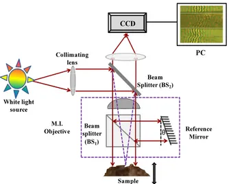
White light source PC Sample M.I. Objective Beam Splitter (BS2) Reference Mirror Beam splitter (BS1) θ Collimating lens CCD
FIG. 1. Schematic diagram of single shot slightly off-axis WL-HPM.
various schemes in WLI, such as, vertical scanning interfero-metry (VSI) [16, 17], phase shifting interferointerfero-metry (PSI) [18-22], fringe projection method [23-27], Fourier profilometry [27, 28], confocal microscope [29]. In the aforementioned methods Linnik, Michelson and Mirau type interferometric objectives are used [12-14].
In the recent past, the color CCD camera has been used to record the color interferogram and color fringe analysis using three laser sources [30-33] or used a phase crossing algorithm to find the phase from a single white light inter-ferogram at a wavelength for which the phase difference between the red, green and blue parts of the white light fringes become equal to zero [34, 35]. This has been extensively used in optical metrology for step height measurement. The phase shifting method, snapshot color fringe projection, digital fringe projection and Fourier transform technique along with phase-crossing methods have been used to extract the phase maps for red, green and blue color interfero-grams [24, 34, 36, 37]. But all these techniques require multiple interferograms to reconstruct the phase, which greatly increases the acquisition and analysis time.
In this paper, we propose single shot white light interfero-metry for 3D step height measurement of Si optoelectronic devices. A white light interferogram is recorded by a low cost single chip color CCD camera as a function of optical path delay. The white light interferogram is decomposed into interferograms of three colors red, blue and green. Individual interferograms of red, green and blue color are separated from white light interferograms recorded by a color CCD camera. A Hilbert transform was used to find the phase map corresponding to each color interferogram. The present technique for determining the wavelength dependent phase doesn’t require multiple color laser sources, spectral filters and dispersive optical elements [30-35]. The system requires only a single chip color CCD camera, white light source and conventional optical microscope. White light scanning interferometry and monochromatic phase- shifting interferometry require a larger number of frames to give a better and more accurate result while in the case of Hilbert phase microscopy (HPM) the retrieval of a full-phase image needs only a single interferogram, which is very useful for dynamic processes and is limited only by recording device response, hence the minimum effect of vibration as compared to phase-shifting interferometry. In addition, a single chip CCD camera reduces the cost and is important for possible commercial use and HPM inherently allows for robust phase unwrapping, which facilitates the study of phase objects much larger than the wavelength of light. The obvious disadvantage of the present technique is that it uses a light for illumination and hence the lateral resolving power is still limited by the wavelength of light, while improvements in lenses, software and in utilizing ultraviolet light will further improve this, the color fringe analysis is limited by its application of white light. The measurement results of AFM are compared to the present technique.
II. WORKING PRINCIPLE
The schematic diagram of the single shot slightly off-axis WL-HPM system is based on a compact Michelson interferometer as shown in Fig. 1. Light generated from a low-coherence source is divided into two beams by a beam splitter and propagates into the sample and the reference arms of the Michelson interferometer. The reflected light from the reference mirror and backscattered light from the sample interfere at the beam splitter and is then detected by the charge-coupled device (CCD) camera, and the wave-length dependent interference fringe signal can be expressed as follows [37, 38]. + = ( , ; ) ( , ; ) ) ; , (x y k I x y k I x y k I i i Oi i Ri i +2
[
Ioi(x,y;ki)IRi (x,y;ki)]
1/2 ×exp[
2ki Δd(x,y)+θ]
(1)[
+ + =I x y k m m k y x Ii( , ; i) 1i( , ; i)1 2* * exp(2kiΔd( )
x,y +θ]
(2) where, i ik =2πλ is the wavenumber and λi is the wavelength
for red (i=1), green (i=2) and blue (i=3). IRi(x,y;k)=I1i(x,y;k)
and IOi(x,y;k)=m.I1i(x,y;k) are the reference and object
irradiance distributions, respectively, Δd( yx, ) denotes optical path difference (OPD) between sample and reference arms and θ is the tilt angle.The minimum allowable angle between the reference beam and the object beam direction is given by θmin= arcsin
( )
3Bλ , with B being the highest spatialfrequency in the object [39]. The last term in Eq. (1) is the interference signal which is sinusoidal as a function of
)
modulated and associated with non-uniform illumination so we use a normalization technique to avoid phase error [40]. To extract this phase the spectral interferogram is Fourier transformed, spatially high-pass filtered to isolate the sinusoidal term and eliminate the background components. The filtered sinusoidal term can be expressed as;
[
Δ +θ]
= I x y k m k d k y x Si( , ; i) 2* 1i( , ; i)* *exp2 i (3)The complex analytic signal associated with the real function of S(x,y;k,) can be obtained as follows:
( ( , ; ))}] .{ ) ; , ( [ 2 1 ) ; , ( i i i i i i x y k S x yk j Hilbert S x yk Z = + (4)
In Eq. (3) the imaginary part of the right-hand side stands for a principal-value integral, easily identifiable as the Hilbert transform of Si(x,y;ki).Using Eq. (4) the wrapped phase associated with complex analytic signal
) ; , ( i i x yk Z is calculated as;
(
)
[
]
(
)
[
]
⎭⎬ ⎫ ⎩ ⎨ ⎧ = − i i i i i i Z x y k k y x Z k y x ; , Re ; , Im tan ) ; , ( 1 φ (5)note that Zi(x,y;ki) exhibits rapid phase modulations; )
; ,
( i
i x y k
φ is wrapped. As the Hilbert transform assumes a signal of infinite extent so we need a phase correction process. The calculated phase is
δ
φ
φ
' = + (6)where
δ
is the error, and that depends upon the number of fringe cycles. However, for any value of wavelength we can calculate the error from the look-up table which is used for calculation of corrected phase φ′ [41]. Eq. (6) provides the so-called modulo 2π phase at each pixel, whose value ranges from 0 to 2π. A minimum LP-norm two-dimensional phase unwrapping algorithm is used to obtain the continuous phase map [42].III. EXPERIMENTAL DETAILS
To study the microscopic structures of a test surface having features of different height, it is necessary to combine an interferometer with the optical setup of a microscope. Such an arrangement is shown in Fig. 1. The schematic diagram of single shot off-axis LC-WL-HPM is shown in Fig. 1. We use both a Mirau interferometric objective lens (Model No 503210, 50X/0.55 DI (interferometric, noncontact and multiple beam), WD 3.4 mm, Nikon, Japan) for smaller area, and a high-resolution and Michelson interferometric
objective lens (Model No 426302, 5X/0.13 TI (interferometric, noncontact and multiple beam), WD 9.3 mm, Nikon, Japan) for a larger area. A non-mechanical scanning HPM consists of a broadband low coherence white light source to illuminate the test and reference surfaces. White light from a source was collimated by a lens and was then made incident onto the Michelson interferometer. The incident beam was split into two beams of nearly equal intensity by a beam splitter, one of these beams being directed onto a flat reference mirror and the other onto the specimen surface. The light reflected from the reference mirror and sample interferes at BS1. When observed from the viewing port, interference occurs between the image of the reference mirror and the image of the specimen surface. To increase the fringe density, we tilted the reference mirror by an angle θ . In our experiment the tilt angle is 15° so that DC component and first order can be clearly filtered out. The two beams are recombined at the same beamsplitter and return through the objective and were recorded by single chip color CCD camera. In the case of the Mirau-interferometric objective the object surface was tilted by a small amount. Single-chip color CCD produces color images based on the Bayer color filter combination in which every pixel registers one color per pixel and provides high RGB color-channel selectivity. We are using a single-chip color CCD camera (Artray, IP 150M, Sony ICX 205AK), 10FPS, with total pixels 1024 (H) × 1360 (V) and a pixel size of 6.25 µm. In the present system, a single interferogram is recorded slightly off-axis. The color interferograms are decomposed into their RGB monochromatic components. The single objective lens is the main advantage of the Michelson interferometer, and hence the first order, aberration in the objective does not contribute to errors in the measurement. Another advantage is that a large sample area can be measured at a time because of the wide field of view of the Michelson interferometric objective. This set-up is used to perform the experiment on a Si solar cell. For Si-IC we have used the Mirau interfero-meter objective lens while the other factors were kept constant. Here we tilt the sample stage by θ . For 50X the measured axial resolution and lateral resolution were 3.8 µm and 1.2 µm respectively. The details about resolution and the Mirau interferometric system were mentioned in our previous paper by Anna et al. [10]. We choose a Mirau interferometer [34] over the other types of interferometers because of its compact size which allows us to integrate it into the microscope and both the sample and the reference beams share a nearly common path up to the beam splitter, therefore they carry the same aberrations caused by the microscope objective.
IV. RESULT AND ANALYSIS
White light commonly generated from a tungsten halogen lamp consists of wavelengths spanning from 400 nm - 800 nm. The recording of the spectral distribution of the white light
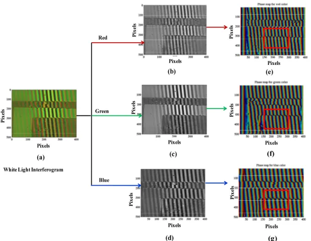
Pixels Pix el s Pixels Pi xe ls Red Green Blue White Light Interferogram
(a) (d) (g) (b) (c) (e) (f) Pi xe ls Pixels Pixels Pix el s Pixels Pi xe ls Pixels Pix el s Pixels Pi xe ls (f) (g)
FIG. 3. (a) WLI of Si-IC using 50X Mirau objective, (b)-(d) red, green and blue interferograms, respectively and (e)-(g) wrapped phase maps, respectively.
FIG. 2. Spectral distribution of white light source (halogen lamp).
source (halogen lamp) with the help of the spectrometer is shown in Fig. 2. White-light interferogram is a mixture of many monochromatic interference fringe patterns and can be decom-posed into three color red, green and blue interferograms. In this section we illustrate the ability of single shot color fringe analysis to provide detailed information about Si-IC and Si solar cell structure. An interference image was obtained and the spatial carrier frequency was increased by introducing
the tilt as shown in Fig. 1 and denoted by a small angle θ. Therefore, high spatial modulation is introduced on the image, which creates well-defined wrapping points on the phase image, thus facilitating the unwrapping procedure. Interference fringes of the sample were recorded by the CCD camera and analyzed using an algorithm written in MATLAB software. The experimental results presented in this paper are the phase images and height variations of Si-IC using 50X Mirau objectives for higher magnification and 5X Michelson interfero-metric objective for for the Si solar cell to obtain the larger area. The object (silicon IC) was placed on the object stage of the microscope and the stage was moved upward to equalize the OPD between the reference and object beam. When the OPD is within the coherence length of the light source the object is also perfectly imaged. Figure 3 (a) shows the WLI of Si-IC using 50X Mirau objective recorded by color CCD camera. It can be seen from Fig. 3(a) that the white light fringe is exactly at the center, this is because for all wavelengths red, green and blue the optical path difference is zero at that position. Beyond the central fringe on both sides the fringes become colored. The color fringe, which contains lot of information, can be separated and analyzed. A recorded white light interferogram of the silicon IC circuit shown in Fig. 3 (a), red (λ0 = 620 nm), green (λ1
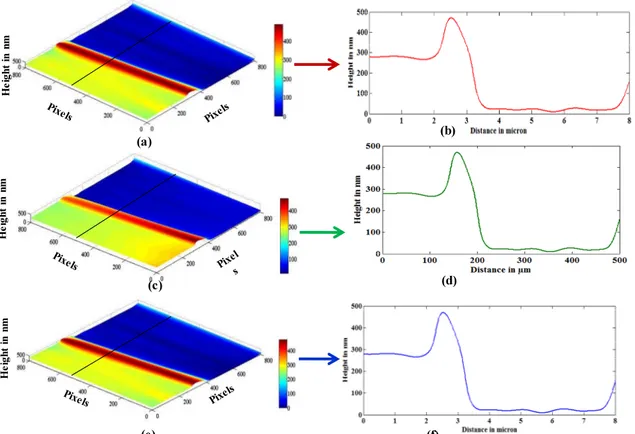
He ig ht in n m (c) (b) (d) (f) He ig ht in n m (a) (e) He ig ht in n m
FIG. 4. (a) and (b) the height map and height profile of Si-IC correspond to red, (c) and (d) correspond to green and (e) and (f) correspond to blue wavelength.
light interferogram were decomposed by a MATLAB program. A Fourier transform was then computed for each color separately. The DC component from the Fourier spectrum was removed for each wavelength and the inverse Fourier transform was then computed to obtain the sinusoidal signal. The complex analytical signal is formed with the help of a Hilbert transform. The wrapped phase map can be obtained using Eq. (6), and the phase was unwrapped using a MATLAB code. The phase difference can be expressed as;
)] , ( 2 [ 2 ) , ( ' x y hi x y i i λπ φ = Δ (7)
where, λi is the center wavelength, hi(x, y) is the height
of the object and i = 1, 2 and 3 for red, green and blue-, respectively. As can be seen from interferograms shown in Fig. 3 (a), (b), and (c), fringes are shifted more than 2π, hence height variation must be larger than,
so phase
ambiguity arises. A minimum LP-norm two-dimensional phase unwrapping algorithm is used to remove the phase ambiguity [42]. A red light interferogram of the object is shown in Fig. 3(b). A wrapped phase map of the interfero-gram was obtained by the Hilbert transform method as shown in Fig. 3(e). By using phase unwrapping methods we can remove the phase ambiguity. Height-map can be determined
by following the equation )] , ( [ 4 ) , (x y ' x y hi i φi π λ Δ = (8)
where, λ1 = 620 nm is the wavelength of red light and Δ
φ ’1 (x, y) is the unwrapped phase map for the red color
wavelength (i = 1). From Eq. (8) the reconstructed step height comes out to be 464 nm for the red wavelength whose height map and profile are shown in Figs. 4(a) and (b), respectively, for a smaller portion of Si-IC shown in the red color box in Fig. 3(e). A similar procedure has been repeated for the green and the blue color wavelengths. For green and blue color wavelengths, interferograms of the object are shown in Figs. 3(c) and 3(d), respectively. and their wrapped phase maps are shown in Figs. 3(f) and 3(g), respecti-vely. From Eq. (8) the reconstructed step height comes out to be 462 nm and 460 nm for green (540 nm) and blue (460 nm) color wavelengths whose height maps and profiles are shown in Fig. 4(c), 4(d) for green and 4(e), 4(f) for blue for the smaller portion of Si-IC shown by red color in Figs. 3(f) and 3(g), respectively. As can be seen from the Figs. 4 (b), (d), and (f) there is a small difference in reconstructed step height, it is due to variation in refractive index with respect to wavelength. The area that we are able to reconstruct is 500 × 500 µm2.
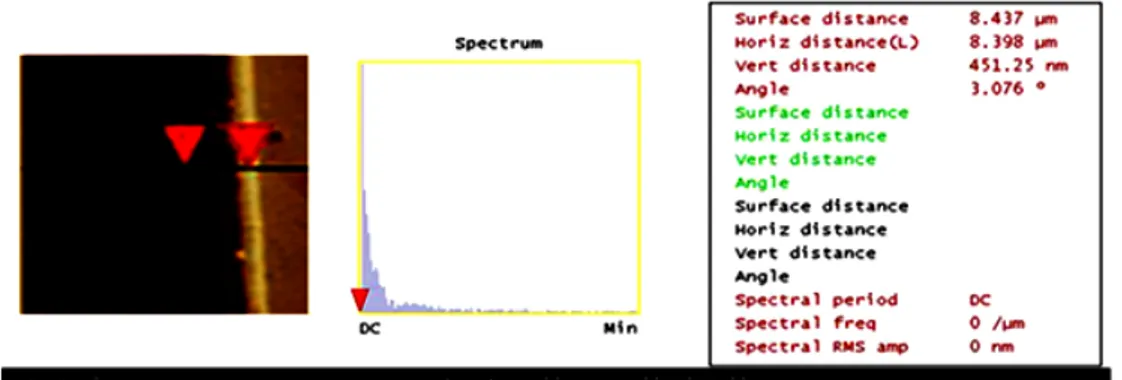
FIG. 5. AFM result of Si-IC.
(a) (b)
(c) (d)
FIG. 6. (a) Si-solar cell interferogram corresponding to red color wavelength by using 5X Michelson objective, (b) wrapped phase map, (c) height map and (d) height profile.
To compare the accuracy of step height measured using Hilbert transform color fringe analysis we have used an atomic force microscopy (AFM) method for step height measurement of the silicon IC circuit. AFM image of the silicon IC circuit was recorded. The height profile was taken along the same pixels in the AFM detection. It has been found that the step height of the silicon IC circuit from AFM was 451 nm shown in Fig. 5. It can be seen that the quantita-tive experimental result of the proposed method is in agreement with the AFM result. The accuracy of AFM is much higher than our technique but the main disadvantages of AFM are that it is a contact method, takes a long time to reconstruct the height profile of a large area of the sample, can only image a maximum height on the order of 10-20 µm and a maximum scanning area of about 150 × 150 µm2 and can also damage the sample. The scanning speed of an AFM is also a limitation. In contrast, white light interfero-metry is well suited to measuring large surface areas rapidly with high precision and very high vertical resolution, with the ability to gather data for surfaces too rough to be examined by techniques such as AFM. Being a non-contact
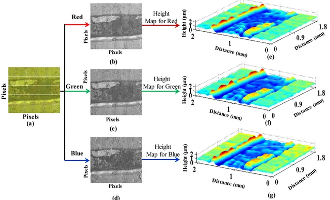
method it avoids the risk of substrate damage and the large field of view gives more representative data, especially for coated surfaces, which tend to exhibit variations in surface quality. The present experimental system was tested for 3D-step height measurement and surface inhomogeniety of a Si solar cell using a 5X Michelson interferometer. 5X Michelson interferometric objective was chosen to image a larger area of the sample. A white light interferogram of the Si solar cell was recorded by a color CCD camera. The colored fringes are separated and analyzed. Recorded white light interferogram of the Si solar cell is decomposed into R, G and B colors in a similar manner as described above. A similar procedure was followed to obtain the height profiles for three different R, G, B colors as described above. It can be clearly seen from the height profile of the Si solar cell for three different colors that there is lot of inhomogenity, surface defects, digs, scratches etc. From the Fig. 6(d) the step height between the electrode and the Si surface is also visible. For red color wavelength (620 nm) the average step height between the electrode and Si surface comes out to be 1.05 nm whose interferogram, phase map,
(a) (b)
(c) (d)
FIG. 7. (a) Si solar cell interferogram corresponding to green color wavelength by using 5X Michelson objective, (b) wrapped phase map, (c) height map and (d) height profile.
(a) (b)
(c) (d)
FIG. 8. (a) Si solar cell interferogram corresponding to blue color wavelength by using 5X Michelson objective, (b) wrapped phase map, (c) height map and (d) height profile.
height map and line profile are shown in Figs. 6(a), (b), (c) and (d), respectively. A similar procedure has been repeated for the green and the blue color light. The green and blue color interferograms of the object are shown in Fig. 7(a) and Fig. 8(a), respectively. Their wrapped phase maps are shown in Figs. 7(b) and 8 (b), respectively. Using Eq. (8) the average step height between the electrode and Si-IC surface comes out to be 0.95 nm and 0.87 nm for
green (540 nm) and blue (460 nm) color wavelengths, respecti-vely. Their height maps and line profiles are shown in Figs. 7(c), 8(c) and 7(d), 8(d), respectively. The area that we are able to reconstruct is 2 mm × 0.5 mm in a single shot. Hence, we can construct a large area in a single shot which is the main advantage of the present technology. We also measured the height variation with a standard optical profiler and found 1.07 µm, which is in close agreement
(a) (b)
FIG. 9. (a) Si solar cell height map for synthetic wavelength ΛRG by using 5X Michelson objective. (b) Height profile for ΛRGand λR.
Red
Green
Blue
Height Map for Red
Height Map for Green
Height Map for Blue (a) (d) (g) Pi xe ls Pi xe ls Pi xe ls Pi xe ls Pixels Pixels Pixels Pixels He ig ht ( µm ) (b) (c) (e) (f) He ig ht ( µm ) He ig ht ( µm )
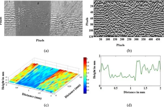
FIG. 10. (a) WLI of Si solar cell using 5X Michelson objectives, (b)-(d) red, green and blue interferograms, respectively and (e)-(f) corresponding height maps.
with our results, as the height variation is less than 2 µm. So, we apply a phase subtraction method Z
RG G R Λ = −φ π φ 4
to avoid phase ambiguity [32, 46-48]. Figure 9(a) shows the height map for synthetic wavelength Λ and Fig. 9(b) RG shows the height variation of Si solar cell. In Fig. 9(b) the red color shows height variation for the red color wavelength which is obtained by removing the phase ambiguity while the black color shows the height variation by using the phase subtraction method which doesn’t have a phase ambiguity since variation in height is less than
2
RG
Λ . But the profile obtained from the phase subtraction
method is noisy because the SNR is wavelength dependent [48]. Further, a large area can be easily reconstructed by means of laterally scanning the object in steps of 2 mm × 0.5 mm and recording a single white interferogram at each step and stitching all the single shot interferograms together. An image mosaicing algorithm based on a random corner method was used to stitch the various adjacent interferograms [49]. Figure 10(a) shows the stitched white light interferogram recorded by a color CCD camera. Figure 10(b) shows the decomposed R, G, B, color interferograms. Figure 10(c) shows the reconstructed step-height of the stitched interferogram for R, G, B, wavelengths. In this way we can reconstruct the large area 2 × 1.8 mm2 of the sample.
However, the present system has poorer resolution as compared to the three-chip color CCD camera. In the three-chip CCD camera for red, blue and green color wavelength there is pixel-by-pixel registration of photons and the lateral spatial resolution is high as compared to the single-chip color CCD camera [48]. But in the present case for the application in Si-ICs and Si solar cells resolution is sufficient and the other drawback of the present technique is cross-talk due to larger spectral width of Bayer color filters which can be avoided by using the three-chip color CCD camera. The repeatability seems to have been limited by the influence of the mechanical vibrations introduced to the optical system. The present technique is highly useful for determining the refractive index of transparent multilayer structures at three different wavelengths. This could be vital for biological samples as well as industrial objects like organic or polymer solar cells and organic light emitting diodes.
V. CONCLUSION
We have demonstrated the real-time single shot Hilbert transform white light interferometry for surface profilometry of a Si-IC and a Si solar cell using Hilbert transform color fringe analysis. The present technique requires only a single chip color CCD camera, a white light source and a conven-tional optical microscope. Three sets of interferograms corres-ponding to R, G, B, colors are obtained from a single white light interferogram and the phase maps corresponding to each interferogram were reconstructed for three wavelengths. Height profiles of the Si-IC and the Si solar cell was then computed for three R, G, B, wavelengths and results were compared with AFM results and found to be in close agreement. The present technique is non-invasive, full-field and fast for the determination of surface profile and surface inhomogeneities of the objects at multiple wavelengths.
ACKNOWLEDGEMENTS
Financial assistance from Department of Science and Technology Delhi, Govt. of India for the project No. SR/S2/ LOP-0021/2008 is gratefully acknowledged.
REFERENCES
1. O. Sasaki and H. Okazaki, “Sinusoidal phase modulating interferometry for surface profile measurement,” Appl. Opt. 25, 3137-3140 (1986).
2. B. S. Lee and T. C. Strand, “Profilometry with a coherence scanning microscope,” Appl. Opt. 29, 3784-3788 (1990). 3. T Dresel, G Häusler, and H Venzke “Three-dimensional
sensing of rough surfaces by coherence radar,” Appl. Opt. 31, 919-925 (1992).
4. P. J. Caber “Interferometric profiler for rough surfaces,”
Appl. Opt. 32, 3438-3444 (1993).
5. T. C. Strand and Y. Katzir “Extended Unambiguous Range Interferometry,” Appl. Opt. 26, 4274-4281 (1987).
6. S. Mirza and C. Shakher, “Surface profiling using phase
shifting Talbot interferometric technique,” Opt. Eng. 44,
013601-013606 (2005).
7. S. S. C. Chim and G. S. Kino “Three-dimensional image
realization in interference microscopy,” Appl. Opt. 31,
2550-2553 (1992).
8. B. L. Danielson and C. Y. Boisrobert “Absolute optical ranging using low coherence interferometry,” Appl. Opt. 30, 2975-2979 (1991).
9. T. Anna, S. K. Dubey, C. Shakher, A. Roy, and D. S. Mehta, “Sinusoidal fringe projection system based on compact and non-mechanical scanning low-coherence Michelson interfero-meter for three-dimensional shape measurement,” Opt. Comm. 282, 1237-1242 (2009).
10. T. Anna, V. Srivastava, D. S. Mehta, and C. Shakher, “High resolution full-field optical coherence microscopy using Mirau interferometer for the quantitative imaging of biological cells,” Appl. Opt. 50, 6343-6351 (2011).
11. B. Bowe and V. Toal, “White light interferometric surface
profiler,” Opt. Eng. 37, 1796-1799 (1998).
12. J. C. Wyant, “White light interferometry,” Proc. SPIE 4737, 98-107 (2002).
13. G. S. Kino and S. S. C. Chim, “Mirau correlation microscope,” Appl. Opt. 29, 3775-3783 (1990).
14. P. de Groot and L. Deck, “Surface profiling by analysis of white-light interferograms in the spatial frequency domain,” J. Mod. Opt. 42, 389-401 (1995).
15. R. Dai, T. B. Xie, and S. P. Chang, “A Scanning White-Light Interferometric Profilometer for Smooth and Rough Surface,”
Key Eng. Mater. 364, 364-370 (2007).
16. L. M. Smith and C. C. Dobson, “Absolute displacement measure-ments using modulation of the spectrum of white light in a
Michelson interferometer,” Appl. Opt. 28, 3339-3342 (1989).
17. B. Bhushan, J. C. Wyant, and C. L. Koliopoulos, “Measurement of surface topography of magnetic tapes by mirau
interfero-metry,” Appl. Opt. 24, 1489-1497 (1985).
18. Z. Buchta, B. Mikel, J. Lazar, and O. Číp, “White-light fringe detection based on a novel light source and colour CCD camera,” Meas. Sci. and Tech. 22, 094031-094036 (2011). 19. P. Sandoz, “An algorithm for profilometry by white-light
phase-shifting interferometry,” J. Mod. Opt. 43, 1545-1554 (1996).
20. M. Li, C. Quan and J. C. Tay “Continuous wavelet transform for micro-component profile measurement using vertical scanning interferometry,” Opt. Laser Technol. 40, 920-929 (2008).
21. V. Srinivasan, H. C. Liu, and M. Halioua, “Automated phase-measuring profilometry of 3-D diffuse objects,” Appl.
Opt. 23, 3105-3108 (1984).
22. H. Su, J. Li, and X. Su, “Phase algorithm without the influence of carrier frequency,” Opt. Eng. 36, 1799-1805 (1997).
23. X. Su, W. Zhou, G. V. Bally, and D. Vukicevic, “Automated phase-measuring profilometry using defocused projection of a Ronchi grating,” Opt. Commun. 94, 561-573 (1992). 24. M. Pawlowski, Y. Sakano, Y. Miyamoto, and M. Takeda,
Opt. Commun. 260, 68-72 (2006).
25. Z. Zhang, D. P. Towers, and C. E. Towers, “Snapshot color fringe projection for absolute three-dimensional metrology of video sequences,” App. Opt. 49, 5947-5953 (2010). 26. D. A. Zweig and R. E. Hufnagel, “Hilbert transform
algorithm for fringe-pattern analysis,” Proc. SPIE 1333, 295-302 (1990).
27. M. Takeda, H. Ina, and S. Kobayashi, “Fourier-transform method of fringe-pattern analysis for computer-based topography and interferometry,” J. Opt. Soc. of Am. 72, 156-160 (1982). 28. K. Qian, H. Wang, and W. Gao, “Windowed Fourier transform
for fringe pattern analysis: theoretical analyses,” App. Opt. 47, 5408-5419 (2008).
29. R. Green, J. Walker, and D. Robinson, “Investigation of the Fourier-transform method of fringe pattern analysis,”
Opt. Lasers Eng. 8, 29-44 (1988).
30. X. Su and W. Chen, “Fourier transform profilometry: a
review,” Opt. Lasers Eng. 35, 263-284 (2001).
31. M. Davidson, K. Kaufman, I. Mazor and F. Cohen, “An application of interference microscopy to integrated circuit inspection and metrology in Integrated Circuit Microscopy,”
Proc. SPIE 775, 233-247 (1987).
32. J. M. Desse, F. Albe, and J. L. Tribillon, “Real-time color holographic interferometry,” Appl. Opt. 41, 5326-5333 (2002). 33. J. M. Desse, “Three-color differential interferometry,” Appl.
Opt. 36, 7150-7156 (1997).
34. J. M. Dessel, P. Picart and P. Tankam, “Digital three-color holographic interferometry for flow analysis,” Opt. Express 16, 5471-5480 (2008).
35. A. Pförtner and J. Schwider “Red-Green-Blue interferometer for the metrology of discontinuous structures,” Appl. Opt. 42, 667-673 (2003).
36. H. C. Hsu, C. H. Tung, C. F. Kao, and C. C. Chang, “A white-light profiling algorithm adopting the multiwavelength interferometry technique,” Proc. SPIE 5531, 244-249 (2004). 37. Z. Buchta, P. Jedlička M. Matějka, V. Kolařík, B. Mikel,
J. Lazar, and O. Číp, “White-light interference fringe detection using color CCD camera,” in Proc IEEE AFRICON 2009 (Safari Park Hotel, Kenya, Sep. 2012), pp. 1-5.
38. S. Zhang and P. Huang, “High-resolution, real-time three-
dimensional shape measurement,” Opt. Eng. 45, 123601-123608
(2006).
39. K. Khare, P. T. S. Ali, and J. Joseph, “Single shot high
resolution digital holography,” Opt. Express 21, 2581-91
(2013).
40. S. K. Debnath, M. P. Kothiyal, and S. W. Kim, “Evaluation of spectral phase in spectrally resolved white-light interfero-metry: Comparative study of single-frame techniques,” Opt. Lasers Eng. 47, 1125-1130 (2009).
41. U. Paul Kumar, N. Krishna Mohan, and M. P. Kothiyal, “Characterization of micro-lenses based on single interferogram analysis using Hilbert transformation,” Opt. Commun. 284, 5084-5092 (2011).
42. D. C. Ghiglia and L. A. Romero, “Minimum Lp-norm
two-dimensional phaseunwrapping,” J. Opt. Soc. of Am. A 13, 1999-2013 (1996).
43. T. Ikeda, G. Popescu, R. R. Dasari, and M. S. Feld, “Hilbert phase microscopy for investigating fast dynamics in transparent systems,” Opt. Lett. 30, 1165-1167 (2005). 44 Y. Verma, P. Nandi, K. D. Rao, M. Sharma, and P. K.
Gupta, “Use of common path phase sensitive spectral domain optical coherence tomography for refractive index measure-ments,” Appl. Opt. 50, E7-E12 (2011).
45. J. Schmit and P. Hariharan, “Two-wavelength interferometry profilometry with a phase-step error– compensating algorithm,” Opt. Eng. 45, 115602-115605 (2006).
46. Y. Y. Cheng and J. C. Wyant, “Multiple-wavelength phase-
shifting interferometry,” Appl. Opt. 24, 804-807 (1985).
47. K. Creath “Step height measurement using two-wavelength phase-shifting interferometry,” Appl. Opt. 26, 2810-2816 (1987). 48. Ma. Suodong, C. Quan, R. Zhu, J. Tay, and L. Chen, “Surface profile measurement in white-light scanning interferometry using a three-chip color CCD,” Appl. Opt. 50, 2246-2254 (2011).
49. D. K. Jain, G. Saxena, and V. K. Singh, “Image Mosaicing Using Corner Techniques,” in Proc 2012 International Con-ference on Communication Systems and Network Technologies (Gujarat, India, May 2012), pp. 79-84.