SOT write schemes with effect of shape
deformation
Cite as: AIP Advances 11, 015035 (2021); https://doi.org/10.1063/9.0000116
Submitted: 15 October 2020 . Accepted: 30 November 2020 . Published Online: 21 January 2021
J. Byun, D. H. Kang, and M. Shin COLLECTIONS
Paper published as part of the special topic on 65th Annual Conference on Magnetism and Magnetic Materials, 65th Annual Conference on Magnetism and Magnetic Materials, 65th Annual Conference on Magnetism and Magnetic Materials, 65th Annual Conference on Magnetism and Magnetic Materials and 65th Annual Conference on Magnetism and Magnetic Materials
ARTICLES YOU MAY BE INTERESTED IN
The design and verification of MuMax3
AIP Advances
4, 107133 (2014);
https://doi.org/10.1063/1.4899186
Field-free and sub-ns magnetization switching of magnetic tunnel junctions by combining
spin-transfer torque and spin–orbit torque
Applied Physics Letters
118, 092406 (2021);
https://doi.org/10.1063/5.0039061
Spin transfer torque devices utilizing the giant spin Hall effect of tungsten
Applied Physics Letters
101, 122404 (2012);
https://doi.org/10.1063/1.4753947
Switching performance comparison between
conventional SOT and STT-SOT write schemes
with effect of shape deformation
Cite as: AIP Advances 11, 015035 (2021);doi: 10.1063/9.0000116
Presented: 6 November 2020 • Submitted: 15 October 2020 • Accepted: 30 November 2020 • Published Online: 21 January 2021 J. Byun, D. H. Kang, and M. Shina)
AFFILIATIONS
School of Electrical Engineering, Korea Advanced Institute of Science and Technology, Daejeon 34141, South Korea Note:This paper was presented at the 65th Annual Conference on Magnetism and Magnetic Materials.
a)Author to whom correspondence should be addressed:[email protected]
ABSTRACT
We demonstrate the effect of shape deformation in spin–orbit torque magnetoresistive random access memory (SOT-MRAM) based on micromagnetic simulation by generating 1000 randomly deformed samples using the exponentially decaying autocorrelation function. The conventional in-plane magnetic field-assisted SOT write scheme and the recently proposed spin-transfer torque-spin-orbit torque (STT-SOT) hybrid write scheme were simulated and compared with the effect of the Gilbert damping constant (α) considered in the presence and the absence of the Dzyaloshinskii–Moriya interaction (DMI). We found that shape deformation of the MTJ can result in write failure or degra-dation of the switching time. To compensate the device-to-device performance variation induced by the shape deformation, the condition of high α and the presence of the DMI is desired for the magnetic field-assisted write scheme. The STT-SOT shows slight improvement in the switching performance for larger α and the presence of DMI while it retains 100% switching probability even with small α regardless of the DMI.
© 2021 Author(s). All article content, except where otherwise noted, is licensed under a Creative Commons Attribution (CC BY) license (http://creativecommons.org/licenses/by/4.0/). https://doi.org/10.1063/9.0000116
I. INTRODUCTION
The magnetic tunnel junction (MTJ) is a promising memory cell due to its non-volatility and good compatibility with current CMOS technology.1 Memory devices using MTJs, such as spin-transfer torques-magneto resistive random access memory (STT-MRAM), have been proposed as a novel L4 cache2 and embed-ded memory.3 However, STT-MRAM is known to have reliability and read disturbance problems because the write and read current both flow through the tunneling barrier of the MTJ. Spin–orbit torque (SOT) is the advanced magnetization reversal scheme of the MTJ,4 which involves in-plane current flowing in the heavy metal layer with high spin–orbit coupling adjacent to the ferro-magnetic free layer and the current produces in-plane spin–orbit torque due to the spin Hall effect and/or Rashba effect.5,6 SOT-MRAM is considered a promising non-volatile upper-level cache memory because of its enhanced life-time and superior switching speed in comparison to STT-MRAM.7Because in SOT-MRAM the read/write paths are decoupled, the tunneling barrier degradation
due to write operation and read disturbance is alleviated.7Moreover, an enhanced switching time of less than 1 ns was experimentally demonstrated.8
The superior switching speed of SOT-MRAM is attributed to the fact that its in-plane torque is exerted on the perpendicular mag-netized MTJ (pMTJ) with negligible incubation time.9 However, because the magnetization is laying in the equator with both paral-lel and anti-paralparal-lel states being stable, SOT alone cannot guarantee deterministic switching because both perpendicular states are stable because of the magnetic anisotropy. Generally, an in-plane magnetic field is applied to tilt the magnetization toward the opposite axis so that the magnetization can switch to the targeted direction.4,8
The newly proposed STT-SOT write scheme10,11suggests that deterministic switching of SOT-MRAM does not necessarily require an in-plane magnetic field. Unlike the conventional magnetic field–assisted write method, the STT-SOT write scheme uses STT to produce constant perpendicular torque towards the targeted direc-tion, which will ensure deterministic switching during the relaxation process. The STT-SOT write scheme can be used in a relatively
MRAM because there is no need to produce an in-plane magnetic field.
For SOT-MRAM to be used in practical memory applications, it is advisable to have a low switching time distribution. For that pur-pose, the process variation, which can affect the switching time, must be addressed. An earlier study of SOT-MRAM using the STT-SOT write scheme found that SOT-MRAM is likely to suffer from the pro-cess variation of the MTJ.11However, the imperfect shape of the MTJ was addressed as the resistance difference in the MTJ rather than the shape deformation effects on switching characteristics despite the fact that the boundary roughness of the ferromagnetic material is known to affect the magnetization reversal process.12
Here, we present a micromagnetic simulation result of shape deformation due to the edge roughness effect in SOT-MRAM. We used randomly generated deformed samples based on the expo-nentially decaying autocorrelation function in the consideration of damping constant variations under the presence or absence of the Dzyaloshinskii–Moriya interaction (DMI).
II. METHODOLOGY
Micromagnetic simulations using the object oriented micro-magnetic framework (OOMMF)13 were conducted to inves-tigate the switching process of SOT-MRAM by solving the Landau–Lifshitz–Gilbert (LLG) equation. The simulated structures are shown inFig. 1(a). The circular MTJ used for the reference had a free layer with a diameter of 60 nm and a 1 nm thickness.
The free layer was perpendicularly (z-direction) magnetized, having initially the +z-direction (parallel-state). Heavy metal placed on the top of the free layer provided the SOT current having the spin polarization along the −y-direction. The roughness generation process is presented inFig. 1(b). The exponentially decaying auto-correlation function is a well-known roughness generation model,
FIG. 1. (a) SOT-MTJ used in the simulation, (b) roughness generation process and result, (c) diameter variation of the generated 1000 samples.
Symbol Parameters Value
α Gilbert damping constant 0.02 to 0.14 Aex Exchange constant 20 ×10−12J/m
H Spin torque efficiency 0.7
θSH Spin Hall angle 0.3
Ku1free Anisotropy constant of the free layer 9.3 ×10⁵J/m3
Msat Saturation magnetization 1.2 ×10 6A/m
Mesh size 1 ×1×1 nm3
which is used to model the roughness of cylindrical structures, such as Silicon-nanowire14or contact edges.15 This function used to generate roughness is expressed as:
R(ϕ) = Δm2exp(−
√ 2 Lm
r∣ϕ∣), (1)
wherer is the radius of the MTJ, ϕ is the in-plane angular compo-nent of the spherical coordinate, Δmis the root mean square (rms)
fluctuation of the roughness, and theLm is the correlation length.
The power spectrum density (PSD) was obtained from the autocor-relation function and, the random phase factor was multiplied to the square root of the PSD to generate the MTJ roughness. Here, Δm=2.5 nm andLm=5 nm were chosen to express the experimental result,3which showed critical dimension (CD) difference less than ± 5% in 3σ. Then 1000 samples were generated with an average diam-eter of 61.78 nm having a ± 5% difference in 3σ. The diamdiam-eter was obtained by fitting an ellipse to a deformed sample to follow the method used in critical dimension-scanning electron microscopy (CD-SEM).16
The switching of the initially perpendicular (z-direction) mag-netization was defined asmz<-0.9 with the simulation time of 5 ns. An in-plane magnetic field ofHx=15 mT and an SOT current den-sity (JSOT) of 9 ×10¹¹A/m2with an SOT current pulse width (TSOT)
of 1 ns were used for the magnetic field-assisted write scheme, and JSOT of 9 ×10¹¹A/m2 withTSOT of 1 ns and STT current density
JSTTof 3 ×10¹⁰A/m2withTSTTof 5 ns were used for the STT-SOT
write scheme. TheTSOTwas chosen to be shorter than theTSTTas
the SOT current has the in-plane torque so the longer STT current pulse should be used to finish the switching to the opposite perpen-dicular state.10T
STTwas chosen to be longer thanTSOTto ensure the
switching of the STT-SOT write scheme. A square current pulse was assumed, and the field-like torque of both SOT and STT were not considered. The DMI was implanted by using OOMMF extension module,17and a Dzyaloshinskii–Moriya (DM) constant of 5 mJ/m2
was applied for the case that considered the DMI. The rest of the parameters used in the simulation are presented inTable I. III. RESULTS AND DISCUSSION
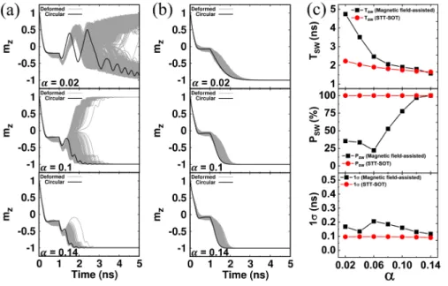
A. In the absence of the DMI
The simulation results of the SOT-MTJ in the absence of the DMI are presented inFig. 2. When the Gilbert damping constant (α) was less than 0.14, the magnetic field-assisted field write scheme was unable to produce 100% switching, while a high damping constant
FIG. 2. Simulation results of the SOT-MTJ in the absence of the DMI. Time evolution of the perpendicular component of the magnetization (mz) of
(gray line) the deformed MTJ samples and (black line) the circular MTJ samples using the (a) magnetic field-assisted write scheme and (b) STT-SOT write scheme with Gilbert damping constant
α = 0.02, 0.1, and 0.14. (c) Average
switching time (TSW), number of
switched samples represented as a percentage (PSW), and distribution 1σ
of the switching time of (black line) magnetic field-assisted write scheme and (red line) STT-SOT write scheme in the variation ofα.
resulted in low variation and enhanced switching speed as seen in
Fig. 2(c). It is known that a relatively low α induces an unstable mag-netization trajectory due to the high precession amplitude, which has been explained as the hysteric behavior of the transition to the inter-mediate position.18–20Such behavior can be observed inFig. 2(a), which shows the time evolution of the perpendicular component of the magnetization (mz) of the SOT-MTJ in the absence of the
DMI using the magnetic field-assisted write scheme. The magnetiza-tion showed highly precessional switching behavior, which resulted in low switching probability. As α increased from 0.02 to 0.14, the switching performance improved because of the faster energy dis-sipation towards the energy minimum (−z) state with high α.21 The average switching time (TSW) decreased from 4.74 ns to 1.57
ns with aTSWdevice-to-device variation 1σ decreases from 0.17 ns
to 0.12 ns and a switching probability (PSW) increases from 35.2%
to 100%.
For the STT-SOT write scheme, shape deformation did not induce switching failure even with low α. This is attributed to the fact that the perpendicular torque induced from the STT was directed towards the −z-axis without the in-plane magnetic field. Thus, less precession around the x-axis was induced with the perpendicular torque of STT suppressing the switching failure. Moreover, despite the fact that the critical STT current (Jc,STT) increased with α, the
switching performance of STT-SOT write scheme enhances with the increment of α. Here, TSWincreased from 2.23 ns to 1.65 ns and 1σ
decreased from 0.1 ns to 0.09 ns when α increased from 0.02 to 0.14. However,TSWwas not as large as that of the magnetic field-assisted
write scheme because the magnetization was located closer towards the x-y plane and relatively far from the −z-direction in the interme-diate state. Thus, the switching speed of magnetic field-assisted write scheme exceeded that of the the STT-SOT write scheme in α = 0.14 asTSWof the magnetic field-assisted write scheme was 1.57 ns, while
theTSWof the STT-SOT write scheme was 1.65 ns.
The source of the device-to-device variation of the switching time can be interpreted as the critical dimension (CD) difference of
the ellipse. the demagnetizing field (HD) of the elliptic thin film is
analytically stated as follows:22 HD=NM, N = ⎡ ⎢ ⎢ ⎢ ⎢ ⎢ ⎣ Nx Ny Nz ⎤ ⎥ ⎥ ⎥ ⎥ ⎥ ⎦ (2)
where N denotes the demagnetizing tensor. With the thickness t much smaller than the minor axis b and major axis a, the demag-netizing factors can be approximated as follows:22
Na=πt 4a[1 − 1 4 a − b a − 3 16( a − b a ) 2 ], Nb=πt 4a[1 − 5 4 a − b a − 21 16( a − b a ) 2 ], Nc=1 −Na−Nb, (3)
The in-plane component of the demagnetization field is there-fore initially negligible because the magnetization of the pMTJ in the relaxed state has small a in-plane magnetization component because of the perpendicular anisotropy. However, due to the interplay of the JSOT,JSTT, and in-plane magnetic field, the magnetization is located
near the in-plane when the SOT pulse is off. Therefore, the shape deformation in the x-y plane of the MTJ will have a larger impact at the beginning of the relaxation process, resulting in device-to-device variation of the switching time. Also, past simulation work indicates that variation of the in-plane magnetic field in the magnetic field-assisted write scheme can result in switching back behavior of the magnetization,23so write failure can be induced by the difference in the in-plane demagnetization field.
FIG. 3. Simulation results of the SOT-MTJ including the DMI term. Time evo-lution of the perpendicular component of the magnetization (mz) of (gray line)
the deformed MTJ samples and (black line) the circular MTJ samples using the (a) magnetic field-assisted write scheme and (b) the STT-SOT write scheme with Gilbert damping constantα = 0.02, 0.1,
and 0.14. (c) Average switching time (TSW), the number of switched samples
represented as a percentage (PSW), and
distribution 1σ of the switching time of
(black line) magnetic field-assisted write scheme and (red line) STT-SOT write scheme in the variation of theα.
B. Inclusion of the DMI
Inclusion of the DMI with a DM constant of 5 mJ/m2resulted in a tendency similar to that of the case without the DMI as seen in
Fig. 3. The STT-SOT write scheme still retained the 100% switch-ing with variance of α, and the magnetic field-assisted write scheme showed better switching characteristics with higher α. The PSW
increased from 49.1% to 100%, while theTSWdecreased from 2.82
ns to 1.38 ns with the 1σ decreases from 0.33 ns to 0.04 ns as α increases from 0.02 to 0.14. Increase of α also enhanced the switch-ing performance of the STT-SOT write scheme. TheTSWdecreased
from 2.06 ns to 1.47 ns, and 1σ decreased from 0.12 ns to 0.09 ns. Compared to the case without the DMI, the presence of the DMI enhanced the switching performance of the magnetic field-assisted write scheme because the magnetization was located closer to the −z-axis in the intermediate state.24However, no drastic performance enhancement of the STT-SOT write scheme due to the DMI was observed although the DMI induced magnetization of the STT-SOT write scheme at the beginning of the relaxation process to be located closer to the −z-axis. An earlier study attributed the degradation of STT efficiency in the presence of the DMI to the DMI-induced non-uniform magnetic texture.25 As a result, with the DMI, the magnetic field-assisted write scheme exceeded the switching perfor-mance of the STT-SOT write scheme when α was higher than 0.8. At a high α of 0.14, the TSWof the magnetic field write scheme was
0.1 ns faster than that of the STT-SOT write scheme with very small device-to-device variation of the magnetization trajectory as seen in
Fig. 3(a)and (b).
In the presence of the DMI, the switching process of SOT-MRAM involves asymmetric edge nucleation and propagation of the domain wall (DW) towards the opposite domain as the nucleated domain expands.9,18,26Nucleation and propagation of the domain can be affected by the edge roughness of the MTJ12which can result in device-to-device variation of the switching performance.Fig. 4
shows the DW propagation process altered by the edge roughness.
Fig. 4(a)shows the MTJ with an edge notch of 6 nm × 9 nm at the corner, which results in the write failure shownFig. 4(b). Although
α = 0.04 assures switching of a circular MTJ, switching of the
deformed sample is not guaranteed with thePSW of 88.3%. The
edge notch hinders DW propagation, and the switching failure occurs as seen inFig. 4(c). The result is consistent with the ear-lier numerical work of SOT switching with the DMI which pro-posed unstable switching behavior when α is low.18The source of the non-deterministic switching of the previous study was thermal fluctuation combined with the increasing tendency of oscillations
FIG. 4. Write failure of the magnetic field-assisted write scheme induced by the edge notch in the presence of the DMI. (a) MTJ with an edge notch of 6 nm ×9 nm (b) perpendicular component of the magnetization (mz), and (c) snapshots
of the magnetization dynamics of the circular MTJ (top) and the MTJ with notch (bottom) whenα = 0.04.
with decreasing α. The DW propagation hindrance can be the source of write failure when α is not high enough, and because the edge roughness of the MTJ can also alters the speed of the DW, it can also be a source of the device-to-device variation of the switching time.
IV. CONCLUSION
Our results indicate that shape deformation of the MTJ may have a crucial effect on the performance of SOT-MRAM: The edge roughness can alter the switching characteristics of SOT-MRAM. For the conventional magnetic field-assisted write scheme, the deformation of the MTJ can result in unstable switching and high device-to-device variation with low α. Hence, a high α was pre-ferred because it can compensate the edge roughness effect, showing less device-to-device variation with enhanced switching probabil-ity and switching speed. On the other hand the STT-SOT write scheme shows 100% of samples switched even at low α. Although Jc,STT is proportional to α, the STT-SOT write scheme also shows
enhanced behavior with higher α; however, the improvement of the switching performance is smaller than that of the magnetic field-assisted write scheme. Our results suggest that the STT-SOT write scheme is preferable if α is low. On the contrary, the SOT-magnetic field write scheme can be a better option if α is high and DMI is present because it shows faster switching speed with determinis-tic switching and there is no need for the write power to produce STT.
ACKNOWLEDGMENTS
This work was supported by the Samsung Research Funding & Incubation Center of Samsung Electronics under Project No. SRFC-IT1901-11.
DATA AVAILABILITY
The data that support the findings of this study are available from the corresponding author upon reasonable request.
REFERENCES
1P. Barla, V. K. Joshi, and S. Bhat,IEEE Access
8, 6876–6889 (2020).
2J. G. Alzateet al., in 2019 IEEE International Electron Devices Meeting (IEDM)
(IEEE, 2019).
3
K. Leeet al., in 2019 IEEE International Electron Devices Meeting (IEDM) (IEEE, 2019).
4M. Cubukcuet al.,Appl. Phys. Lett.
104, 042406 (2014).
5P. M. Haney, H. W. Lee, K. J. Lee, A. Manchon, and M. D. Stiles,Phys. Rev. B 87, 174411 (2013).
6
X. Fan, H. Celik, J. Wu, C. Ni, K. J. Lee, V. O. Loreanz, and J. Q. Xiao,Nat. Commun.5, 3042 (2014).
7G. Prenatet al.,IEEE Transactions on Multi-Scale Computing Systems 2, 49–60 (2016).
8
K. Garelloet al., in 2018 IEEE Symposium on VLSI Circuits (IEEE, 2018).
9
M. Baumgartneret al.,Nat. Nanotechnol.12, 980–986 (2017).
10
S. Pathak, C. Youm, and J. Hong,Sci. Rep.10, 2799 (2020).
11
B. Zeinali, J. K. Madsen, P. Raghavan, and F. Moradi, in2017 IEEE International Conference on Computer Design (ICCD) (IEEE, 2017).
12D. Meyners, H. Brückl, and G. Reiss,J. Appl. Phys.
93, 2676 (2003).
13R. McMichael and M. Donahue, “OOMMF user’s guide, version 1.0,”
Inter-agency Report NISTIR 6376, National Institute of Standards and Technology, Gaithersburg, MD, USA, 1999.
14H.-E. Jung and M. Shin,IEEE Trans. Electron Devices
60, 1861–1866 (2013).
15Y. Ban, Y. Ma, H. J. Levinson, and D. Z. Pan,J. Micro/Nanolithography, MEMS,
MOEMS9, 041211 (2010).
16
T. Ohashiet al.,J. Micro/Nanolithography, MEMS, MOEMS17, 024002 (2018).
17
S. Rohart and A. Thiaville,Phys. Rev. B88, 184422 (2013).
18
N. Mikuszeitet al.,Phys. Rev. B92, 144424 (2015).
19
B. Chenet al.,IEEE Magn. Lett.7, 3105205 (2016).
20
S. Wang, M. Yang, and C. Zhao,IEEE Magn. Lett.9, 3101804 (2018).
21
Z. Wang, Z. Li, M. Wang, B. Wu, D. Zhu, and W. Zhao,Nanotechnology30, 375202 (2019).
22D. D. Tang and Y.-J. Lee, inMagnetic Memory: Fundamentals and Technology
(Cambridge University Press, 2010), Chap. 3, pp. 52–53.
23
Y.-J. Tsou, J.-C. Chiu, H.-C. Shih, and C. W. Liu,IEEE J. Explor. Solid-State Computat.5, 173–181 (2019).
24B. Chen, J. Lourembam, S. Goolaup, and S. T. Lim,Appl. Phys. Lett.
114, 022401 (2019).
25
Y. Gao, Z. Wang, X. Lin, W. Kang, Y. Zhang, and W. Zhao,IEEE Trans. Nanotechnol.16, 1138–1142 (2017).
26E. Martinezet al.,Sci. Rep.