Organic
flash memory on various flexible
substrates for foldable and disposable electronics
Seungwon Lee
1, Hyejeong Seong
2, Sung Gap Im
2, Hanul Moon
1& Seunghyup Yoo
1With the emergence of wearable or disposable electronics, there grows a demand for aflash memory realizable on various flexible substrates. Nevertheless, it has been challenging to develop a flash memory that simultaneously exhibits a significant level of flexibility and performance. This is mainly due to the scarcity offlexible dielectric materials with insulating properties sufficient for a flash memory, which involves dual dielectric layers, respectively, responsible for tunneling and blocking of charges. Here we report ultra-flexible organic flash memories based on polymer dielectrics prepared by initiated chemical vapor deposition. Using their near-ideal dielectric characteristics, we demonstrate flash memories bendable down to a radius of 300μm that exhibits a relatively long-projected retention with a programming voltage on par with the present industrial standards. The proposed memory technology is then applied to non-conventional substrates, such as papers, to demonstrate its feasibility in a wide range of applications.
DOI: 10.1038/s41467-017-00805-z OPEN
1School of Electrical Engineering, Korea Advanced Institute of Science and Technology (KAIST), Daejeon 34141, Republic of Korea.2Department of Chemical & Biomolecular Engineering, KAIST, Daejeon 34141, Republic of Korea. Correspondence and requests for materials should be addressed to
F
lash memory is a non-volatile, transistor-based data-storage device that has become essential in most electronic systems found in modern daily life. With straightforward operation mechanisms and easy integration into NAND or NOR array architectures,flash memories have been established as by far the most successful and dominant non-volatile memory technology1,2. Above all, their direct electrical programming requiring no mechanical parts greatly reduces the weight of an overall system as well as the power consumption, making it hugely popular in portable electronics spanning from thumb drives and memory cards to solid-state drives in smart phones and laptops1, 2. Emerging areas, such as wearable, body-attachable, or disposable electronics, will also greatly benefit from such characteristics of flash memories as well as from their well-established circuit infrastructure, provided that they can be realized on various non-rigid substrates and, at the same time, can exhibit a memory performance that is sufficient for real-world applications3–12. In these respects, many studies have been devoted to the development offlash memories based on organic or other emerging electronic materials that can potentially be compatible with flexible substrates13–22.Despite promising demonstrations in the early stages13–36, however, the overall progress in thisfield has been far slower than that of thin-film transistors (TFTs) or other devices based on
flexible materials37–46. Major challenges lie in the core structure offlash memories, which involves dielectric bilayers sandwiching a charge storage layer such as a floating gate (FG) electrode (Fig.1a). In addition to playing a regular role as a gate insulator, these two dielectric layers have to provide a reliable and controllable means by serving, respectively, (i) as a tunneling dielectric layer (TDL) through which to inject charges into the FG for programming or to remove charges therefrom for erasing via control of a control gate (CG) bias; and (ii) as a blocking dielectric layer (BDL) to prevent charge leakage to confine the stored charges within the FG for memory retention and to ensure that chargeflow occurs only through the TDL during program-ming/erasing (Fig. 1b)1, 2. For reasonably low-programming/ erasing voltages, these dielectric layers should not be made too thick; this unfortunately contradicts the conditions for long memory retention in many cases. A best-case scenario would thus be to use dielectric layers that are thin enough to enable low-voltage programming/erasing and yet can provide leak-free insulating properties even at such small thickness. Finding such an ideal dielectric layer has been very difficult for polymeric layers, which are the most prominent candidate material for flexible electronics47–50. The solution processing used for most polymeric dielectric layers also makes it difficult to use them in flash memories due to the complexity involved in the formation
Electron BDL (pEGDMA) CG (Al) FG (Al) TDL (pV3D3) Channel (C60) S/D Source Drain Channel FG CG TDL BDL Substrate Al Ca 50 nm BDL (kBDL) TDL (kTDL) CG FG dBDL dTDL S eVBDL Channel Fermi level (EF) Poly(1,3,5-trimethyl-1,3,5-trivinyl cyclotrisiloxane) (pV3D3)
Normal (initial) state
a b c Erased state Programmed state Programming Erasing
Poly(ethylene glycol dimethacrylate) (pEGDMA) O Si O Si O Si O Si O Si O Si * * O O O O * * * * (total) eVTDL (total)
Fig. 1 Structure of thin-film transistor-based organic flash memories and their operation mechanism. a The schematic device structure of the proposed flash memory and a false-color cross-sectional TEM image of the fabricated flash memory device. TDL, BDL, CG, FG, and S/D refer to tunneling dielectric layer, blocking dielectric layer, control gate,floating gate, and source/drain, respectively. b Energy band diagrams of the flash memory device under study for various operation regimes. The total voltages across BDL (=VBDL(total)) and TDL (=VTDL(total)) are determined by the various factors such as built-in voltages, applied VCG, and coupling ratio, Vthshift due to stored or depleted charges, etc., as described in details in Supplementary Table1.c Chemical structures of the poly(1,3,5-trimethyl-1,3,5-trivinyl cyclotrisiloxane) (pV3D3) and the poly(ethylene glycol dimethacrylate) (pEGDMA) polymers used as TDL and BDL, respectively
of the bilayer dielectric structure, which is the key to flash memory operations. All of these considerations have made it highly challenging to realize trueflash memories in flexible form factors.
Herein, we try to overcome these hurdles and realize highly flexible flash memories by employing thin polymeric insulators grown with initiated chemical vapor deposition (iCVD), a vapor-phase growth technique for polymers pioneered by Gleason and her coworkers51. With tunneling-limited characteristics, these dielectrics have recently been demon-strated as flexible gate insulators that are important for low-voltageflexible TFTs52. In this work, it is further shown that the iCVD-based polymeric insulators can make a significant contribution to flash memories as well. With a rational design and material choice that carefully consider both applied and built-in electric fields across the dielectric layers for each operating condition, the proposed approach simultaneously enables long retention (projected to be ~>10 years) and low-programming/erasing voltages comparable to the present
industrial standards (~±10 V). We then take full advantage of the mild, solvent-free, and low-temperature growth of iCVD to demonstrate flexible flash memories on various non-rigid substrates including ultrathin plastics and paper.
Results
Design and characterization of organic flash memories. The proposed non-volatile memory devices are based on C60-based organic TFTs, wherein the gate insulator is replaced with a TDL/FG/BDL, as shown in the schematic device structure presented in Fig. 1a. C60 was chosen mainly for its consistency that led to a mobility larger than 1 cm2V−1s−1 with a good run-to-run reproducibility53–56. Two iCVD processed polymer films of poly(1,3,5-trimethyl-1,3,5-trivinyl cyclotrisiloxane) (pV3D3) and poly(ethylene glycol dimethacrylate) (pEGDMA)52, whose chemical structures are shown in Fig. 1c, are employed for TDL and BDL, respectively. While pV3D3 was chosen for its excellent insulating properties and down scalability that had
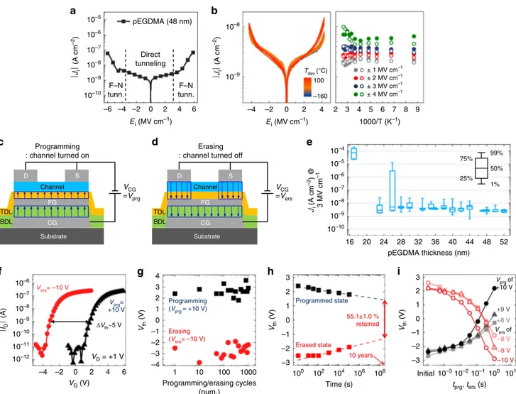
Vprg of +10 V Vers of +9 V +8 V –8 V –9 V –10 V Programming (Vprg = +10 V) Erasing (Vers= –10 V) 55.1±1.0 % retained 10 years Programmed state Erased state Vprg= +10 V Vers= –10 V ΔVth~5 V ± 1 MV cm–1 ± 2 MV cm–1 ± 3 MV cm–1 ± 4 MV cm–1 Tdev (°C) 100 –160 Direct tunneling F–N tunn. F–N tunn. S D Channel FG Substrate BDL CG TDL VCG =Vprg VCG =Vers Programming : channel turned on S D Channel FG Substrate BDL CG TDL Erasing
: channel turned off 75% 99%
50% 25% 1% 10–5 a b c d e f g h i pEGDMA (48 nm) 10–6 10–7 10–8 10–9 ⎪Ji ⎪ (A cm –2) ⎪lD ⎪ (A) ⎪Ji ⎪ (A cm –2) Ji (A cm –2) @ 3 MV cm –1 Vth (V) Vth (V) 10–10 –6 –4 –2 0 10–4 10–5 10–6 10–7 10–8 10–9 10–10 20 16 10–6 4 3 3 2 1 0 –1 –2 –3 Vth (V) 3 2 1 0 –1 –2 –3 2 1 0 –1 –2 –3 –4 10–7 10–8 10–9 10–10 10–11 10–12 –4 –2 0 2 4 6 1 10 100 Programming/erasing cycles (num.) Time (s) 1000 100 10–3 tprg, ters (s) Initial 10–210–1100 101 102 104 106 108 24 28 32 36 pEGDMA thickness (nm) 40 44 48 52 2 4 2 3 4 5 6 7 8 9 –4 –2 0 Ei (MV cm–1) Ei (MV cm –1 ) VG (V) VD = +1 V 1000/T (K–1) 2 4 6 10–8 10–9
Fig. 2 Properties of iCVD-processed polymer dielectric layers and an organicflash memory made thereof on plastic substrates. a |Ji| vs. Eicharacteristics of a Al/pEGDMA (48 nm)/Al device. The vertical, dashed lines are a guide to eyes that divides low-field, direct-like tunneling regime and high-field, Fowler–Nordheim (F–N)-like tunneling regime. The latter can be easily distinguished from the low-field regime due to the clear field-enhanced Jiover Ei. In both regimes, it is likely that each tunneling mechanism is coupled with trap-assisted tunneling (TAT)57,58.b|Ji|–Eicharacteristics of Al/pEGDMA (36 nm)/Al devices measured at various device temperatures (Tdev) (left) and Arrhenius plots (right) transformed from them.c, d Sketches of electricfield (shown as arrows) distribution insideflash memory under programming (c) and erasing (d) operations. e Statistical distribution of Jiat Eiof 3 MV cm−1 obtained for the Al/pEGDMA/Al devices with various pEGDMA thicknesses.f–i Device characteristics of the proposed flash memories fabricated on a PET substrate: transfer memory characteristics (f), endurance test result over repeated programming/erasing operations (g), data retention characteristics (h), and memory speed characteristics for various programming/erasing voltages (i). All the transistor and memory characteristics in Fig.2and those appearing later have been measured under controlled atmosphere in an N2-filled glove box, unless specified otherwise
previously been reported by Moon et al.52, pEGDMA was selected not only for its consistent insulating performance comparable to that of pV3D3, but also for its dielectric constant larger than that of pV3D3, which will be discussed later in details. As can be seen in the false-color high-resolution transmission electron microscopy (HRTEM) image in Fig. 1a, these polymers make a conformal coating on the bumpy Al surfaces used as a CG and a FG, respectively, thanks to the characteristics inherent to the vapor-based iCVD method. This conformal growth is highly beneficial in the present case because it can minimize a chance of forming accidental electrical short paths. Like pV3D352, pEGDMA polymer layers also have superb insulating properties even onflexible substrates, with low leakage current density (Ji) and a relatively high breakdownfield of over 6 MV cm−1(Fig.2a). This is due not only to the conformal coverage but also to the tunneling-limited insulating properties of iCVD-based polymers, which are characteristic to near-ideal dielectric layers with low trap densities52. The tunneling-limited behavior can be verified from their Jivs. applied electricfield (Ei) characteristics, which are almost independent of the device temperature over a wide range, as shown in ref. 51 for pV3D3 and in Fig. 2b for pEGDMA.
From the viewpoint of memory operation, the Ji–Ei character-istics of a metal-insulator-metal (MIM) device with near-ideal dielectric layers may be divided into two distinctive regions as shown for pEGDMA in Fig. 2a: (i) a low-Ei regime where Ji is significantly low due to direct-like tunneling where tunneling should be made through a full barrier width; and (ii) a high-Ei regime where Ji exhibits field-enhanced behavior, due to Fowler–Nordheim (F–N)-like tunneling, which involves tunneling throughfield-induced triangular barriers. It should be noted that, in both regimes, each tunneling mechanism could be further assisted with trap-assisted tunneling (TAT) found in dielectrics like high-quality Al2O357,58, where a localized trap can help the respective tunneling processes by playing a role like that of a“stepping stone.” Staying in the low-Ei region is important in terms of memory retention, while utilizing field-enhanced, F–N-like tunneling can become critical for programming and erasing. Hence, it is crucial to ensure the field across TDL (=ETDL) is high enough during programming/erasing so that Jiis dominated by F–N-like tunneling. On the other hand, the field across BDL (=EBDL) should always remain low to prevent charges fromflowing through BDL in all the cases and to let charges flow into or out from FG only through TDL, if necessary for programming or erasing. To fulfill these seemingly conflicting conditions simultaneously, it is necessary to first look at the voltages across BDL (=VBDL) and TDL (=VTDL) and the associated EBDL and ETDL when a bias (=VCG) is applied to a CG with respect to a source (S) and drain (D) electrodes. EBDL and ETDLare linked to each other via the so-called coupling ratio (αCR= VFG/VCG) and thus depend on the properties of both BDL and TDL, rather than solely on the properties of their own dielectric layers. Consider, for simplicity’s sake, an S/TDL/FG/ BDL/CG structure, which is equivalent to the memory structure underneath S electrode except for the absence of a semiconductor layer. Under capacitive approximation and in the absence of a built-in field, it can be shown that ETDL/EBDL scales with kBDLABDL/(kTDLATDL), where kiand Ai(i= BDL or TDL) are the relative dielectric constant and area of the insulating layers under study (see Supplementary Fig. 1and Supplementary Note 1for further details). pEGDMA used as a BDL in this work was found to have a k value of 3.059, which is significantly higher than that of pV3D3 used as a TDL (=2.2). This tends to make it easy for the condition of ETDL> EBDL to be met at a given VCG for programming/erasing, and thus provides a foundation to realize the required asymmetry between carrier flows though BDL and
TDL. It is noteworthy that the dielectric constant of parylene, a polymer produced from vapor phase and commonly used in many areas, is on par with that of pEGDMA. Hence parylene could also be used for a BDL in this scheme. One concern for parylene is, however, its relatively low break-down field60. Nevertheless, the report by Song et al. demonstrates that the dielectric properties of polymers could be significantly improved upon use of soft contacts such as transferred graphene61. If the break-downfield of parylene can further be increased in this way, parylene may also be used as one of the gate dielectric layers for memory devices.
Once kTDLand kBDLare chosen, one needs to determine the thicknesses of BDL (=dBDL) and TDL (=dTDL) that can fulfill thefield requirements for all the memory operation conditions. In the real memory structure (instead of the aforementioned simplified case), the detailed energy band alignment should be carefully taken into account, because it can lead to built-infields across BDL and TDL and thus exert an influence on the net field across those layers. It should further be noted that the built-in fields vary depending on the memory state because they are influenced by the differential increase or decrease in the amount of charge confined within FG (see Supplementary Table 1and description therein for further details). Another complication, which results from the inherent properties of a typical organic TFT, is the change inαCRassociated with the dependence of the capacitance of the FG/TDL/channel/S(D) structure (=CTDL) on the operation modes. Due to the gate-modulated conductivity of the channel, the effective thickness and area determining CTDL during programming (i.e., channel is ON) are dTDLand the area underneath the channel that overlaps with FG, respectively; in contrast, those relevant to the erasing process (i.e., channel is OFF) are dTDLplus the channel thickness (dchannel) and the area underneath D and S electrodes overlapping with FG, respectively (Fig.2c, d). The energy diagrams in Fig.1b were constructed by considering the location of Fermi level for C60and its interfacial alignment with Ca62, the spatial distribution of the vacuum level shift associated with the confined charges, the applied VCG (if any), and operation-mode-dependent αCR, etc. With a BDL thicker than a TDL (in this work, dBDL/dTDL= 1.8–5), energy diagrams are configured in such a way that F–N-like tunneling can occur efficiently across TDL, while it is much less effective for BDL due either to the low net electric field (during the programming operation; Fig. 1b “programming”) or to the energy barrier configuration, which is relevant to direct tunneling instead of F–N tunneling (during the erasing operation; Fig. 1b “erasing”).
When choosing dTDLand dBDL, it should also be kept in mind that these values should be larger than the critical thickness (=dcrit) of the corresponding dielectric layer, below which the layer’s insulating properties will quickly be degraded47, 63. A statistical study done for pEGDMA-based MIM devices fabricated in several batches indicates that dcrit of pEGDMA is ca. 30 nm (Fig. 2e). We have thus adopted the pEGDMA layer that is at least thicker than ca. 30-40 nm. With dcrit of pV3D3 being ca. 10 nm52, the total dielectric thickness can be maintained within 50–68 nm. With this total thickness, we were able to keep the programming and erasing voltages (Vprgand Vers) relatively low while still fulfilling all the requirements mentioned above. For example, the proposed flexible organic flash memory with 40 nm-thick pEGDMA and 16 nm-thick pV3D3 on PET substrates exhibited transistor characteristics that can be switched on at less than 3 V; the device also showed a sufficient voltage shift (ΔVth) of ~5 V with Vprgand Versas low as±10 V (Fig.2f). Note that these levels ofΔVthand programming/erasing voltages are comparable to those of conventional Si-basedflash memory devices2, 64. With |Δnfg| = CBDL×|ΔVth|/e, wherein Δnfg and e
refer to the change in carrier density stored in FG and charge of an electron, respectively, the observed ΔVthcorresponds toΔnfg of 2.1 × 1012cm−2, which is on par with those of mostflash-like memories found in the literature (see Supplementary Table 2). The reason why Δnfg exhibits little variation among different devices, albeit their widespreadΔVth, is that aflash memory with lower CBDLgenerally requires higher operating voltages and thus demands higherΔVthfor proper memory operation, making the CBDLΔVthproduct (and thus Δnfg) remain in the similar range among different systems. In addition, the flexible memory devices in this study showed reliable programming and erasing behaviors for repetitive operations of 1000 times (Fig. 2g and Supplementary Fig.2).
Moreover, the proposed memory devices exhibited significantly long retention time (tret), estimated to be 3.2 × 10⁸s (≈10 years), during which over 50% of the initial ΔVth is projected to be preserved (Fig.2h). As can be seen in the energy diagram given in Fig.1b) for“Programmed state”, presence of the stored charges in FG tends to yield band bending in energy bands for both TDL and BDL. Because their slopes are still relatively small, however, thefield across the insulators remain within the low-field regime. In this case, tunneling probability can be maintained low enough to enable long retention, provided that there are no other leakage paths such as electrical shorts. The observed level of large tretis thus consistent with tunneling-limited insulating properties of pV3D3 and pEGDMA used in this work. Nonetheless, one should
Programming (Vprg = +8 V) Erasing (Vers = –10 V) Initial “Relaxed” Push “Folded” Memory dev. Piano wire (R = 300 μm) Pull Affixed f g Vth (V) 4 3 2 1 0 –1 –2 101
Folding cycles (num.) 102 103 –4 –2 0 2 4 10–12 10–11 10–10 ⎪ID ⎪, ⎪IG ⎪ (A) 10–9 10–8 10–7 10–6 Initial state Folded state VG (V) VD = +1 V Erased states Programmed
states Folded memory test config.
S D Probes for CG Source (S) tip Drain (D) tip Control gate (CG) tip Piano wire ( R = 300 μ m) 500 μm Probe for S Probe for CG Probe for D Folded dev. under test Piano wire d e 6 8 10 S CG D Org. After 1200 foldings Initial Programming (Vprg = +8 V) Erasing (Vers = –8 V) Programming (Vprg = +9 V) Erasing (Vers = –9 V) R = 4.7 mm Strain = 1.1% 2 a b 3 c 20 15 10 5 0 0 1 2 3 4 2 1 0 –1 –2 –3 –4 1 0 –1 Vth (V) Vth (V) Ji @ 3 MV cm –1 (nA cm –2) –2 0 1 2
Tensile strain (%) Tensile strain (%)
3 101 102
Bending cycles (num.) 103 104
Fig. 3 Characteristics of the proposedflexible flash memory under or after mechanical deformation. a, b Vthmeasured upon programming/erasing operations for devices under various bending induced tensile strains (a), and Vthmeasured after repetitive bending cycles with tensile strain of 1.1% (b), (inset: a photograph of theflexible organic flash memory fabricated on 100 μm-thick PET films). c Jivalues of Al/pEGDMA (40 nm)/Al devices at an Eiof 3 MV cm−1measured as a function of various tensile strains.d Transfer memory characteristics of the proposed memory devices fabricated on 6μm-thick MylarTMsubstrates (“ultrathin Mylar” hereafter) in their flat and folded states, and after 1200-time folding cycles. Folding radius is 300 μm and defined by the radius of a piano wire. Inset shows a photograph of the foldedflash memory fabricated on the MylarTMfilm. e Photograph of a memory device on the ultrathin Mylar being characterized under the folded state. A top-view microscope image and a side-view probing diagram are also presented to show that folding-induced strain is applied exactly along the channel parallel to the long edges of S and D electrodes as shown in the schematic diagram presented in the inset. Such alignment can be witnessed by the contact pads (shown as areas surrounded by the dashed lines) of S and D that are overlapped each other. Note that the probe for S makes a contact from underneath the folded device.f A schematic diagram showing the method for alternating between“relaxed” and“folded” states for measurement of memory characteristics after repeated folding cycles. g Vthof the memory on ultrathin Mylar substrates measued upon programming/erasing operations after repeated folding cycles at 300μm bending radius vs. the number of folding cycles
keep in mind that the quoted retention time is the extrapolated value that considers only the electrical aspects and that the actual memory retention is subject to degradation depending on ambient conditions. The long-term test with proper encapsulation should be made to fully assess their actual retention time in practice. As for programming/erasing speed, the device showed aΔVthof ca. 2 V at tprgand tersas low as 10 ms (Fig.2i), simultaneously fulfilling all the requirements for key performance parameters—reasonably low voltage and short time span for programming and erasing; and sufficiently long retention. Mechanicalflexibility of the proposed organic flash memories. To estimate the mechanical durability of the proposed organic flash memory, a device fabricated on a 250 μm-thick PET substrate was tested as a function of flexural tensile strain by adjusting the bending radius of curvature. The device showed consistent programming/erasing behaviors after flexural deformation corresponding to tensile strain of up to 2.8% (Fig.3a and Supplementary Fig. 3), and it still exhibited memory characteristics even after the 10,000 bending cycles at a flexural strain of 1.1% (Fig.3b and Supplementary Fig.4). This excellent mechanical durability against flexural strain can be attributed to the highlyflexible nature of the iCVD-based polymeric dielectric layers. Both the pEGDMA and pV3D3 dielectric layers maintained their insulating property at tensile strain of up to 4% in a bending test using MIM devices (Fig. 3c, Supplementary Fig. 3, and refs. 51, 52. these results are in sharp contrast to the cases of inorganic dielectric layers that typically lose their insulating property with strain of ~1% in a similar test37.
It is noteworthy that the onset strain for failure (=εonset) is lower for flexible memory devices than for the corresponding flexible MIM devices. This is attributed to the relatively complex device structure of memory devices, which involves a larger number of heterogeneous interfaces than is present in MIM devices. This is consistent with theεonsetvalue of 3.3% obtained for a C60-based TFT transistor having the same configuration as
the proposedflash memory except that Al FG is not included (see Supplementary Fig.5).
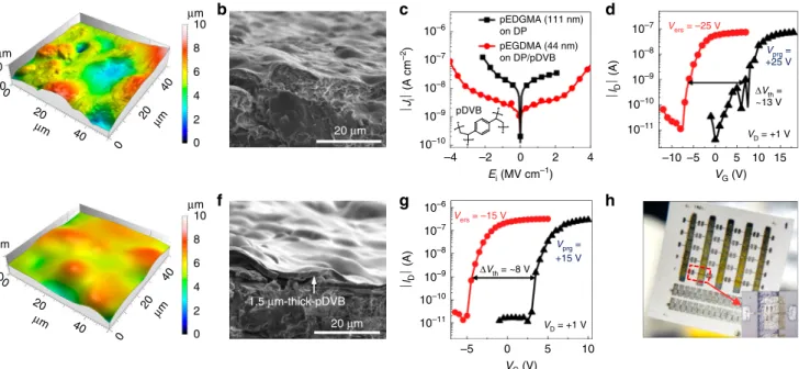
Even with a value of εonset smaller than those of the corresponding TFTs or MIM devices, the observed value is still unprecedented for flexible flash memories13–18 and is large enough to realize ultra-flexible form factors with a thin plastic substrate10,37,39. This will allow for a greater degree of freedom in designing flexible electronic systems, e.g., for wearable or skin-attachable electronic products. To verify this, the memory devices under study were fabricated on 6μm-thick MylarTMfilms using 33 nm-thick pEGDMA as a BDL and 17 nm-thick pV3D3 as a TDL. As can be seen in Fig. 3d, the devices were easily bendable over a needle with the radius of merely 300μm. The resultant devices show non-volatile memory operation comparable to that of the devices prepared on thick PET substrates. As the 6μm-thick plastic substrate significantly reduces the bending-induced strain at its surface, the achievable bending radius can become so small that devices on top of it can almost be folded. When tested with a custom-designed bending machine that can define a sub-mm bending radius with the assistance of a rigid piano wire (Fig. 3e, f, Supplementary Fig.6, and Supplementary Movies1and2), these devices were shown to maintain their programming and erasing capabilities in the folded state as well as after 1200-time folding cycles (Fig. 3d, g) for a bending radius of 300μm. This demonstrates their potential as nearly foldable and light-weightflash memory devices, which will be pivotal for epidermal or imperceptible electronics10,37,39. The possibility of fabricating these devices on MylarTM or PET substrates is a direct benefit of the low-temperature processability of the iCVD process, as these polyester films have relatively low-service temperature and glass-rubber transition temperature. Upon comparison with the previous works, the result shown here can be regarded as a significant breakthrough toward realization of highly flexible flash memory that satisfies both low Vprg, Vers, and long tret(Supplementary Table2and Supplementary Fig.7). 20 μm 20 μm 1.5 μm-thick-pDVB 10 00 20 40 0 20 40 μm μm μm 10 10–6 a b c d h g f e 10–7 10–8 10–9 10–10 10–11 10–7 10–8 10–9 10–10 10–6 10–7 10–8 10–9 10–10 10–11 –4 –5 0 5 10 –10 –5 0 5 10 15 –2 pDVB pEDGMA (111 nm) on DP pEGDMA (44 nm) on DP/pDVB 0 Ei (MV cm–1) VG (V) VG (V) VD = +1 V VD = +1 V ΔVth = ~13 V ΔVth = ~8 V Vprg = +25 V Vprg = +15 V Vers = –25 V Vers = –15 V 2 4 μm 8 6 4 2 0 10 00 20 40 0 20 40 μm μm μm 10 μm 8 6 4 2 0 ⎪Ji ⎪ (A cm –2) ⎪lD ⎪ (A) ⎪lD ⎪ (A) * * * *
Fig. 4 Organicflash memories on papers for disposable electronics. a, b Surface and cross-sectional morphologies of a pristine dye-sublimation paper (DP) characterized with atomic force microscopy (AFM) and scanning electron microscopy (SEM).c Ji–Eicharacteristics of pEGDMA layers measured from Al/ pEGDMA (111 nm)/Al devices fabricated on a pristine DP (black line with squares) and that of Al/pEGDMA (44 nm)/Al on a pDVB-coated DP. The molecular structure of pDVB is shown in the inset.d Transfer memory characteristics of aflash memory fabricated on a pristine DP (dBDL= 111 nm). e, f Surface and cross-sectional morphologies of the pDVB-coated DP.g Transfer memory characteristics of aflash memory fabricated on a pDVB-covered DP (dBDL= 44 nm). h A photograph of the proposed paper-based organic flash memories
Realization of flash memories on papers for disposable elec-tronics. Another advantage of the iCVD process that can be useful forflexible memory devices is its solvent-free nature52,65,66. Together with the conformal coating capability and low-temperature processability, this benefit provides the potential to build memory devices on a wide range of unconventional substrates, including those with a low damage threshold to liquid as well as those with relatively large roughness52, 65,66. In this respect, one attractive yet highly challenging substrate to build memory devices on is paper, which has all the unfavorable conditions mentioned above67–79. To determine whether substrates for the proposed memory can be extended even to paper, we built our devices on so-called dye-sublimation papers (DP), which has a significantly rough surface with bumps in both micro- and nano-scale (Fig. 4a, b and Supplementary Fig. 8). Note that DP does not have a plastic coating unlike the thick specialty photo paper used for inkjet printing of photographs. It was found that, thanks to the conformal coating capability of iCVD, a 111 nm-thick pEGDMA layer exhibited a considerable insulating property even on such a rough DP surface, as shown as a black line with squares in Fig. 4c. An organic flash memory fabricated on the DP surface with the 111 nm-thick pEGDMA-based BDL and a 44 nm-thick pV3D3-pEGDMA-based TDL was shown to be successfully operable with ΔVth of ~13 V for Vprgor Versof ±25 V (Fig.4d).
To further drive down the operation voltage of memory devices on paper, we used the iCVD process to apply a 1.5μm-thick poly (divinylbenzene) (pDVB) layer on the pristine DP surface so that nano-scale bumps were smoothened and only the relatively large micron-scale profiles remained. pDVB was chosen mainly for its relatively high deposition rate (~μm h−1) and, moreover, for its planarizing capability. (Fig. 4e, f and Supplementary Fig.8) In this case, even a 44 nm-thick pEGDMA layer showed a sufficiently good insulating property that was on par with the property observed in devices on glass or plastic substrates, as can be seen as a red line with circles in Fig.4c. With this modification,
the organic flash memory with the 44 nm-thick pEGDMA BDL and a 24 nm-thick pV3D3 TDL showed non-volatile memory operation withΔVthof ca. 8 V at Vprgor Versof±15 V (Fig.4g, h). To the best of our knowledge, this is thefirst demonstration of the flash memories on paper with practically meaningful operation voltage and a sufficient memory window. The results clearly demonstrate the immense potential of the iCVD process forflash memories on almost any kinds offlexible substrates.
Discussion
In summary,flexible organic flash memory devices realized in this work on various substrates exhibit both industry-compatible operating voltage (~10 V) and relatively long-projected retention time. Thanks to the virtue of iCVD-based polymeric insulating layers with a near-ideal insulating property limited by carrier tunneling, an organic flash memory can be designed, in a systematic fashion, based on a TDL/FG/BDL structure. The versatile synthetic capability of the iCVD process makes it possible to choose, from the pool of various iCVD-based polymers, a proper insulator that can meet the conditions that are key to the systematic design (e.g., a TDL with low dcrit; a BDL with a higher dielectric constant than a TDL). Furthermore, the advantages of the iCVD process, such as low process temperature, solution-free nature, and highly conformal deposition, help one to realize flash memories on various flexible substrates such as PET, ultrathin MylarTM, and paper, which would otherwise be highly challenging to build memory devices on. The proposed devices on thick PET substrates are found to be able to withstandflexural strain of up to 2.8%, which is unprecedented
for non-volatile memory devices. It is noteworthy that the proposed approach is not specific to C60, which is known to be air-sensitive and thus subject to degradation without encapsulation; some of the air-stable compounds80,81can also be used provided that their preparation is compatible with flexible substrates of interest. All these advantages are expected to allow non-volatile memories to be fabricated on virtually any flexible substrates while maintaining a sufficient level of performance as well as a high degree of mechanical flexibility. We believe the proposed approach will open a path for forthcoming electronics that are expected to be ubiquitous in daily life by providing an effective means for wearable, foldable, or disposable electronics. Methods
Initiated chemical vapor deposition process. Each of the monomers called ethylene glycol dimethacrylate (EGDMA), 1,3,5-trimethyl-1,3,5-trivinyl cyclotrisilo-xane (V3D3), and divinylbenzene (DVB) was vaporized and delivered to a custom-built iCVD reactor with the initiator, tert-butyl peroxide (TBPO) for the formation of pEGDMA, pV3D3, and pDVB, respectively, via free-radical polymerization reaction. The growth rates of pV3D3, pEGDMA, and pDVB were 1.5, 5, and 15 nm min−1, respectively. The process pressure was maintained at 70–300 mTorr, and the filament was heated to 160–200 °C. The substrate temperature was maintained at 40 °C. The thickness of the deposited polymerfilms was controlled in situ by a He–Ne laser (JDS Uniphase) interferometer system.
Surface andfilm characterization. To observe the cross-sectional structure of the non-volatile organicflash memory devices, the devices were sliced using a dual-beam focused ion beam (FIB, Helios Nanolab 450). HRTEM (Titan cubed G2 60-300) images were then obtained. The surface morphology of the bare dye-sublimation paper (DP) and the DP coated with pDVB was characterized using AFM (Nanosurf Nanite AFM & C3000 controller).
Device fabrication. The glass substrates were cleaned with detergent dissolved in deionized (DI) water, DI water, acetone, and isopropyl alcohol (IPA) successively in an ultrasonic bath for 20 min each, and dried at 100 °C for 12 h in a vacuum oven. PET substrates were cleaned with IPA. Ultra-thin Mylar and DP substrates were not cleaned with solvent; instead, a stream of compressed N2gas was just blown onto the substrates before fabrication.
For the planarization, PET and Mylar substrates were treated with air plasma (CUTE-1MP, Femto Science Inc.) for 1 min at 70 W. Directly after the plasma treatment, PET and Mylarfilms were spin-coated with a transparent photoresist (SU-8, Kayaku Microchem) at 2000 rpm (30 s).
For the fabrication of the bottom-gated C60-based non-volatileflash memory, 100 nm-thick Al as CG was deposited by thermal evaporation with a base pressure lower than 10−6Torr using shadow masks with a deposition rate of ~0.1 nm s−1, and pEGDMA polymer insulators as the BDL were deposited by the iCVD process on the top of CG electrodes with the desired thicknesses. The 15 or 50 nm-thick Al as the FG was then thermally evaporated in the same manner as Al prepared for the CG. pV3D3 polymer insulators as TDL were then deposited by the iCVD process on top of the FG electrodes. The memory devices were then completed by sequential thermal evaporation of 50 nm-thick C60channel layers (~0.07 nm s−1) and Ca (20 nm)/Al(100 nm) layers as source (S) and drain (D) electrodes. Patterns for electrodes were defined with shadow masks.
Electrical characterization of devices. All current density vs. voltage character-istics (J–V) were analyzed using a semiconductor parameter analyzer (HP4155A or HP4156C, Agilent). Electrical characteristics of any devices with C60were measured under controlled atmosphere in an N2-filled glove box unless noted otherwise. Capacitance vs. voltage characteristics (C–V) of MIM devices were measured using a precision LCR meter (HP4284A, Agilent). Dielectric constants (k) were estimated by using the relationship among C, k, and thickness of an insulator, following the procedure described in“Methods” section in the previous work by Moon et al.52. To measure the J–V characteristics of the MIM devices with various values of device temperature (Tdev), the samples were placed on a hot chuck in a customized vacuum chamber with probe tips, and Tdevwas systematically controlled by a combination of liquid N2gasflow and the chuck heating. To evaluate the electrical properties of theflexible (or foldable) MIM and non-volatile memory devices as a function of the bending radius and the number of bending cycles, the devices were tested with a custom-built bending tester. In case of a sub-mm bending radius, a piano-wire was employed and held tightly to maintain a proper tension for straightness. For nearly foldable devices on MylarTMsubstrates, the center of the bending was carefully aligned to the center of individual MIMs and memory devices by using a microscope.
Data availability. All relevant data supporting thefindings of this study are included within the paper and its Supplementary Information File, or available from the corresponding authors on reasonable request.
Received: 28 December 2016 Accepted: 31 July 2017
References
1. Pavan, P., Bez, R., Olivo, P. & Zanoni, E. Flash memory cells-an overview. Proc. IEEE 85, 1248–1271 (1997).
2. Bez, R., Camerlenghi, E., Modelli, A. & Visconti, A. Introduction toflash memory. Proc. IEEE 91, 489–502 (2003).
3. Son, D. et al. Multifunctional wearable devices for diagnosis and therapy of movement disorders. Nat. Nanotechnol. 9, 397–404 (2014).
4. Zeng, W. et al. Fiber‐based wearable electronics: a review of materials, fabrication, devices, and applications. Adv. Mater. 26, 5310–5336 (2014). 5. Wang, X., Gu, Y., Xiong, Z., Cui, Z. & Zhang, T. Silk-moldedflexible,
ultrasensitive, and highly stable electronic skin for monitoring human physiological signals. Adv. Mater. 26, 1336–1342 (2014).
6. Kim, D.-H. et al. Dissolvablefilms of silk fibroin for ultrathin conformal bio-integrated electronics. Nat. Mater. 9, 511–517 (2010).
7. Hwang, S.-W. et al. A physically transient form of silicon electronics. Science 337, 1640–1644 (2012).
8. Kang, S.-K. et al. Bioresorbable silicon electronic sensors for the brain. Nature 530, 71–76 (2016).
9. Salvatore, G. A. et al. Wafer-scale design of lightweight and transparent electronics that wraps around hairs. Nat. Commun. 5, 2982 (2014). 10. Sekitani, T., Zschieschang, U., Klauk, H. & Someya, T. Flexible organic
transistors and circuits with extreme bending stability. Nat. Mater. 9, 1015–1022 (2010).
11. Yi, H. T., Payne, M. M., Anthony, J. E. & Podzorov, V. Ultra-flexible solution-processed organicfield-effect transistors. Nat. Commun. 3, 1259 (2012). 12. Fukuda, K. et al. Fully-printed high-performance organic thin-film transistors
and circuitry on one-micron-thick polymerfilms. Nat. Commun. 5, 4147 (2014).
13. Sekitani, T. et al. Organic nonvolatile memory transistors forflexible sensor arrays. Science 326, 1516–1519 (2009).
14. Kaltenbrunner, M. et al. Anodized aluminum oxide thinfilms for room‐ temperature‐processed, flexible, low‐voltage organic non‐volatile memory elements with excellent charge retention. Adv. Mater. 23, 4892–4896 (2011). 15. Kim, S.-J., Song, J.-M. & Lee, J.-S. Transparent organic thin-film transistors and
nonvolatile memory devices fabricated onflexible plastic substrates. J. Mater. Chem. 21, 14516–14522 (2011).
16. Kim, S. M. et al. Transparent andflexible graphene charge-trap memory. ACS Nano 6, 7879–7884 (2012).
17. Han, S. T. et al. Layer‐by‐layer‐assembled reduced graphene oxide/gold nanoparticle hybrid double‐floating‐gate structure for low‐voltage flexible flash memory. Adv. Mater. 25, 872–877 (2013).
18. Kim, S.-J. & Lee, J.-S. Flexible organic transistor memory devices. Nano Lett. 10, 2884–2890 (2010).
19. Baeg, K. J., Noh, Y. Y., Sirringhaus, H. & Kim, D. Y. Controllable shifts in threshold voltage of top‐gate polymer field‐effect transistors for applications in organic nanofloating gate memory. Adv. Funct. Mater. 20, 224–230 (2010). 20. Mabrook, M. F., Yun, Y., Pearson, C., Zeze, D. A. & Petty, M. C. A
pentacene-based organic thinfilm memory transistor. Appl. Phys. Lett. 94, 173302 (2009). 21. Shih, C.-C. et al. High performance transparent transistor memory devices
using nano-floating gate of polymer/ZnO nanocomposites. Sci. Rep. 6, 20129 (2016).
22. Han, S. T., Zhou, Y. & Roy, V. Towards the development offlexible non‐volatile memories. Adv. Mater. 25, 5425–5449 (2013).
23. Gupta, D., Anand, M., Ryu, S.-W., Choi, Y.-K. & Yoo, S. Nonvolatile memory based on sol-gel ZnO thin-film transistors with Ag nanoparticles embedded in the ZnO/gate insulator interface. Appl. Phys. Lett. 93, 224106 (2008). 24. Novembre, C., Guerin, D., Lmimouni, K., Gamrat, C. & Vuillaume, D. Gold
nanoparticle-pentacene memory transistors. Appl. Phys. Lett. 92, 103314 (2008).
25. Kim, S.-J., Park, Y.-S., Lyu, S.-H. & Lee, J.-S. Nonvolatile nano-floating gate memory devices based on pentacene semiconductors and organic tunneling insulator layers. Appl. Phys. Lett. 96, 033302 (2010).
26. Kim, Y.-M., Kim, S.-J. & Lee, J.-S. Organic-transistor-based nano-floating-gate memory devices having multistack charge-trapping layers. IEEE Electron Dev. Lett. 31, 503–505 (2010).
27. Chang, H. C., Lu, C., Liu, C. L. & Chen, W. C. Single‐crystal C60 needle/CuPc nanoparticle doublefloating‐gate for low‐voltage organic transistors based non‐volatile memory devices. Adv. Mater. 27, 27–33 (2015).
28. Park, Y., Park, S., Jo, I., Hong, B. H. & Hong, Y. Controlled growth of a graphene charge-floating gate for organic non-volatile memory transistors. Org. Electron. 27, 227–231 (2015).
29. Yi, M. et al. The effect of porous structure of PMMA tunneling dielectric layer on the performance of nonvolatilefloating-gate organic field-effect transistor memory devices. Org. Electron. 33, 95–101 (2016).
30. Shih, C. C., Chiu, Y. C., Lee, W. Y., Chen, J. Y. & Chen, W. C. Conjugated polymer nanoparticles as nanofloating gate electrets for high performance nonvolatile organic transistor memory devices. Adv. Funct. Mater. 25, 1511–1519 (2015).
31. Lee, S. Y. et al. Chemically modulated band gap in bilayer graphene memory transistors with high on/off ratio. ACS Nano 9, 9034–9042 (2015). 32. Li, D. et al. Nonvolatilefloating‐gate memories based on stacked black
phosphorus–boron nitride–MoS2 heterostructures. Adv. Funct. Mater. 25, 7360–7365 (2015).
33. Han, S.-T. et al. Two-dimensional molybdenum disulphide nanosheet-covered metal nanoparticle array as afloating gate in multi-functional flash memories. Nanoscale 7, 17496–17503 (2015).
34. Bertolazzi, S., Krasnozhon, D. & Kis, A. Nonvolatile memory cells based on MoS2/graphene heterostructures. ACS Nano 7, 3246–3252 (2013). 35. Liu, Z., Xue, F., Su, Y., Lvov, Y. M. & Varahramyan, K. Memory effect of a
polymer thin-film transistor with self-assembled gold nanoparticles in the gate dielectric. IEEE Trans. Nanotechnol. 5, 379–384 (2006).
36. Lee, S. et al. Overcoming the“retention vs. voltage” trade-off in nonvolatile organic memory: Ag nanoparticles covered with dipolar self-assembled monolayers as robust charge storage nodes. Org. Electron. 14, 3260–3266 (2013).
37. Kaltenbrunner, M. et al. An ultra-lightweight design for imperceptible plastic electronics. Nature 499, 458–463 (2013).
38. Kim, R. H. et al. Non-volatile organic memory with sub-millimetre bending radius. Nat. Commun. 5, 3583 (2014).
39. Yokota, T. et al. Ultraflexible organic photonic skin. Sci. Adv. 2, e1501856 (2016).
40. White, M. S. et al. Ultrathin, highlyflexible and stretchable PLEDs. Nat. Photon 7, 811–816 (2013).
41. Kaltenbrunner, M. et al. Ultrathin and lightweight organic solar cells with high flexibility. Nat. Commun. 3, 770 (2012).
42. Choi, M. K. et al. Wearable red-green-blue quantum dot light-emitting diode array using high-resolution intaglio transfer printing. Nat. Commun. 6, 7149 (2015).
43. Asadi, K., De Leeuw, D. M., De Boer, B. & Blom, P. W. Organic non-volatile memories from ferroelectric phase-separated blends. Nat. Mater. 7, 547–550 (2008).
44. Jeong, H. Y. et al. Graphene oxide thinfilms for flexible nonvolatile memory applications. Nano Lett. 10, 4381–4386 (2010).
45. Yao, J. et al. Highly transparent nonvolatile resistive memory devices from silicon oxide and graphene. Nat. Commun. 3, 1101 (2012).
46. Ji, Y. et al. Flexible and twistable non-volatile memory cell array with all-organic one diode–one resistor architecture. Nat. Commun. 4, 2707 (2013). 47. Facchetti, A., Yoon, M. H. & Marks, T. J. Gate dielectrics for organicfield‐effect
transistors: new opportunities for organic electronics. Adv. Mater. 17, 1705–1725 (2005).
48. Veres, J., Ogier, S., Lloyd, G. & De Leeuw, D. Gate insulators in organic field-effect transistors. Chem. Mater. 16, 4543–4555 (2004).
49. Sirringhaus, H. Device physics of solution‐processed organic field‐effect transistors. Adv. Mater. 17, 2411–2425 (2005).
50. Ling, Q.-D. et al. Polymer electronic memories: materials, devices and mechanisms. Prog. Polym. Sci. 33, 917–978 (2008).
51. Baxamusa, S. H., Im, S. G. & Gleason, K. K. Initiated and oxidative chemical vapor deposition: a scalable method for conformal and functional polymer films on real substrates. Phys. Chem. Chem. Phys. 11, 5227–5240 (2009). 52. Moon, H. et al. Synthesis of ultrathin polymer insulating layers by initiated
chemical vapour deposition for low-power soft electronics. Nat. Mater. 14, 628–635 (2015).
53. Zhang, X.-H., Domercq, B. & Kippelen, B. High-performance and electrically stable C60organicfield-effect transistors. Appl. Phys. Lett. 91, 092114 (2007). 54. Anthopoulos, T. D. et al. High performance n-channel organicfield-effect
transistors and ring oscillators based on C60fullerenefilms. Appl. Phys. Lett. 89, 213504 (2006).
55. Itaka, K. et al. High‐mobility C60field‐effect transistors fabricated on molecular‐wetting controlled substrates. Adv. Mater. 18, 1713–1716 (2006). 56. Schwabegger, G. et al. High mobility, low voltage operating C60based n-type
organicfield effect transistors. Synth. Met. 161, 2058–2062 (2011).
57. Specht, M., Städele, M., Jakschik, S. & Schröder, U. Transport mechanisms in atomic-layer-deposited Al2O3dielectrics. Appl. Phys. Lett. 84, 3076–3078 (2004).
58. Yang, B.-L., Lai, P. & Wong, H. Conduction mechanisms in MOS gate dielectric films. Microelectron. Reliab 44, 709–718 (2004).
59. Seong, H., Pak, K., Joo, M., Choi, J. & Im, S. G. Vapor-phase deposited ultrathin polymer gate dielectrics for high-performance organic thinfilm transistors. Adv. Electron. Mater 2, 1500209 (2016).
60. Kondo, M. et al. Ultraflexible and ultrathin polymeric gate insulator for 2 V organic transistor circuits. Appl. Phys. Express 9, 061602 (2016).
61. Song, J. et al. A general method for transferring graphene onto soft surfaces. Nat. Nanotechnol. 8, 356–362 (2013).
62. Yi, Y. & Kang, S. J. Interfacial electronic structures between fullerene and calcium for high performance n-type organic semiconducting devices. Thin Solid Films 519, 3119–3122 (2011).
63. Cheng, X. et al. Air stable cross-linked cytop ultrathin gate dielectric for high yield low-voltage top-gate organicfield-effect transistors. Chem. Mater. 22, 1559–1566 (2010).
64. Takeuchi, K. Novel co-design of NANDflash memory and NAND flash controller circuits for sub-30 nm low-power high-speed solid-state drives (SSD). IEEE J. Solid State Circuits 44, 1227–1234 (2009).
65. Lewis, H. G. P., Bansal, N. P., White, A. J. & Handy, E. S. HWCVD of polymers: commercialization and scale-up. Thin Solid Films 517, 3551–3554 (2009). 66. Alf, M. E. et al. Chemical vapor deposition of conformal, functional, and
responsive polymerfilms. Adv. Mater. 22, 1993–2027 (2010).
67. Tobjörk, D. & Österbacka, R. Paper electronics. Adv. Mater. 23, 1935–1961 (2011).
68. Andersson, P. et al. Active matrix displays based on all-organic electrochemical smart pixels printed on paper. Adv. Mater. 14, 1460–1464 (2002).
69. Eder, F. et al. Organic electronics on paper. Appl. Phys. Lett. 84, 2673–2675 (2004). 70. Kim, Y.-H., Moon, D.-G. & Han, J.-I. Organic TFT array on a paper substrate.
IEEE Electron Dev. Lett. 25, 702–704 (2004).
71. Fortunato, E. et al. High-performanceflexible hybrid field-effect transistors based on cellulosefiber paper. IEEE Electron Dev. Lett. 29, 988–990 (2008). 72. Zschieschang, U. et al. Organic electronics on banknotes. Adv. Mater. 23,
654–658 (2011).
73. Martins, R. et al. Complementary metal oxide semiconductor technology with and on paper. Adv. Mater. 23, 4491–4496 (2011).
74. Khan, M. A., Bhansali, U. S. & Alshareef, H. N. High‐performance non‐volatile organic ferroelectric memory on banknotes. Adv. Mater. 24, 2165–2170 (2012). 75. Lee, B.-H. et al. Foldable and disposable memory on paper. Sci. Rep. 6, 38389
(2016).
76. Ferreira, I. et al. Solid-state paper batteries for controlling paper transistors. Electrochim. Acta 56, 1099–1105 (2011).
77. Martins, R. F. et al. Recyclable,flexible, low‐power oxide electronics. Adv. Funct. Mater. 23, 2153–2161 (2013).
78. Zhang, L. et al. Substrate‐free ultra‐flexible organic field‐effect transistors and five‐stage ring oscillators. Adv. Mater. 25, 5455–5460 (2013).
79. Pereira, L. et al. The influence of fibril composition and dimension on the performance of paper gated oxide transistors. Nanotechnology 25, 094007 (2014). 80. Takimiya, K. et al. 2, 7-Diphenyl [1] benzothieno [3, 2-b] benzothiophene, a
new organic semiconductor for air-stable organicfield-effect transistors with mobilities up to 2.0 cm2 V-1 s-1. J. Am. Chem. Soc. 128, 12604–12605 (2006).
81. Zschieschang, U. et al. Flexible low‐voltage organic transistors and circuits based on a high‐mobility organic semiconductor with good air stability. Adv. Mater. 22, 982–985 (2010).
Acknowledgements
This work was supported by Samsung Research Funding Center of Samsung Electronics under Project Number SRFC-MA1402-04. H.M. is grateful to Brain Korea 21 Plus Program for post-doctoral fellowship.
Author contributions
S.L., H.S., S.G.I., H.M., and S.Y. designed the experiments on the use of iCVD-based polymers as dielectrics for non-volatile organicflash memory devices. S.L. carried out fabrication and characterization of organicflash memory devices on plastic substrates as well as on paper. H.S and S.G.I. carried out process design, fabrication, and character-ization of iCVD-processed polymerfilms. S.L., H.M., and S.Y. worked on the design and electrical analysis of a device structure and electrical analysis. S.L., H.M., and S.Y. wrote the manuscript. All authors read and commented on the manuscript. H.M. and S.Y. contributed equally as corresponding authors.
Additional information
Supplementary Informationaccompanies this paper at doi:10.1038/s41467-017-00805-z. Competing interests:The authors declare no competingfinancial interests.
Reprints and permissioninformation is available online athttp://npg.nature.com/ reprintsandpermissions/
Publisher's note:Springer Nature remains neutral with regard to jurisdictional claims in published maps and institutional affiliations.
Open Access This article is licensed under a Creative Commons Attribution 4.0 International License, which permits use, sharing, adaptation, distribution and reproduction in any medium or format, as long as you give appropriate credit to the original author(s) and the source, provide a link to the Creative Commons license, and indicate if changes were made. The images or other third party material in this article are included in the article’s Creative Commons license, unless indicated otherwise in a credit line to the material. If material is not included in the article’s Creative Commons license and your intended use is not permitted by statutory regulation or exceeds the permitted use, you will need to obtain permission directly from the copyright holder. To view a copy of this license, visithttp://creativecommons.org/ licenses/by/4.0/.