Date of publication xxxx 00, 0000, date of current version xxxx 00, 0000. Digital Object Identifier 10.1109/ACCESS.2017.Doi Number
A Novel Experimental Approach to the
Applicability of High-Sensitivity Giant
Magneto-Impedance Sensors in Magnetic Field
Communication
JANG-YEOL KIM1, IN-KUI CHO1, HYUN JOON LEE1, JAEWOO LEE1, JUNG-ICK MOON1,
SEONG-MIN KIM1, SANG-WON KIM1, SEUNGYOUNG AHN2, (Senior Member, IEEE), AND
KIBEOM KIM2
1Radio & Satellite Research Division, Electronics and Telecommunications Research Institute, Daejeon 34129, South Korea
2Cho Chun Shik Graduate School of Green Transportation, Korea Advanced Institute of Science and Technology, Daejeon 34051, South Korea
Corresponding author: Kibeom Kim (e-mail: [email protected]).
This work was supported by the Institute of Information & Communications Technology Planning & Evaluation(IITP) grant funded by the Korea government(MSIT) (No.2019-0-00007, Magnetic Field Communication Technology Based on 10pT Class Magnetic Field for Middle and Long Range).
ABSTRACT This paper presents a new application field of a giant magneto-impedance (GMI) sensor. It shows valuable findings for the GMI sensor on the possibility of a new receiving element in magnetic field communication. The proposed GMI sensors serve as antennas and mixers in receiver systems. They have the advantage of being easily implemented and in terms of mass production and manufacturing processes due to the manufacture base on a printed circuit board (PCB). Their smaller size, lower cost, and higher sensitivity have more advantages than conventional magnetic sensors, such as the magneto-inductive, anisotropic magneto-resistive, and giant magneto-resistive sensors. Two types of PCB-based GMI sensors are proposed. The first type of GMI sensor is directly wound around the solenoid-shaped pickup coil onto an alumina insulation tube inserted with an amorphous microwire. The second type of GMI sensor has a patterned pickup coil that does not require the winding of the coil, similar to the patterned pickup coil of a micro electro-mechanical system-based GMI sensor. This GMI sensor provides a new geometry that can be easily manufactured with two PCB substrates. The proposed GMI sensors achieve the equivalent magnetic noise spectral density to the high-sensitivity characteristics of the pT/√Hz level. The equivalent magnetic noise spectral density of 1.5 pT/√Hz at 20.03 MHz is obtained for the first type of GMI sensor, and 3 pT/√Hz at 3.03 MHz is achieved the second type. The analyzed results of the bandwidth and the channel capacity for the two types of GMI sensors are acceptable. This first analysis confirms the possibility of the implementation of GMI sensors in magnetic field communication. The results of this experiment confirm the high performance of the proposed GMI sensors and their applicability in magnetic field communication. The detailed experimental results of the proposed GMI sensors are presented and discussed.
INDEX TERMS Amorphous microwire, giant magneto-impedance (GMI), high sensitivity, magnetic field communication, magnetic sensor.
I. INTRODUCTION
Magnetic sensors play an increasing role in wireless sensor networks. Thus, studies have focused on the applicability of these sensors to wireless communication systems in underground and underwater environments. In these environments, the conventional techniques of using electromagnetic (EM) waves in the gigahertz frequency
band dramatically increase bit error rates. The non-uniform soil, rocks, and water cause high levels of reflection and attenuation of the communication signals, and this results in channel unreliability [1], [2]. Techniques that use the magnetic field can solve these issues. Specifically, the wireless communication problems of multi-path propagation and fading are resolved because most materials,
except nickel, cobalt, and iron, have the same permeability as air. Thus, magnetic communication has low susceptibility to underwater and underground environments.
An important factor in magnetic communication is the increase in voltage conversion ratio, which is expressed in V/T units, to detect weak magnetic fields. Several magnetometers, also known as magnetic sensors, are available. Examples are magneto-inductive (MI), fluxgate, Hall effect, anisotropic magneto-resistive (AMR), giant magneto-resistive (GMR), superconducting quantum interface device (SQUID), and optically pumped (OPM) sensors [3]–[15]. These magnetic sensors are generally known to have high-sensitivity characteristics [3]. High-sensitivity magnetic sensors are widely used in nearly all engineering and industrial areas, such as automobile, high-density magnetic recording, navigation, non-destructive testing, magnetic marking and labeling, military and security, biomagnetic measurements in the human body, meteorological, aviation, and geomagnetic measurement applications [3], [4]. For instance, the MI, fluxgate, and GMR sensors are being used for measuring perturbations in the magnitudes and direction of Earth’s field due to induced or permanent dipoles in major applications of magnetic compasses, munitions fuzing and mineral prospecting [4]. A two-axis fluxgate sensor that could be used in navigation systems is currently being studied [10]. The Hall-effect sensor is used for the application of non-contact switching, magnetic memory readout and current measurements. The AMR sensor is mainly being applied to the magnetic field communication system and flexible electronics [11], [12]. The SQUID sensor is being used for measuring field gradients or differences due to permanent dipole magnets in major applications of brain function mapping and magnetic anomaly detection. In addition, the research on SQUID sensors for application to tomb exploration, airborne transient electromagnetic, and magnetic resonance image
system being reported [13], [14]. The OPM sensor is mainly being studied in the application of biomagnetic measurement for the magnetoencephalogram and the magnetocardiogram, and communication [15]. The trend of magnetic sensor development is toward sensors that are smaller, faster, more affordable, more sensitive, low power consuming, and reliable in order to apply magnetic sensors to the various fields mentioned above. Moreover, magnetic sensors are being used in various applications because they have a high-sensitivity resolution from the nano-tesla level to the femto-tesla level and can detect weak external magnetic fields because of their high-sensitivity characteristics. The magnetic sensors, such as the above, directly convert the magnetic field into voltage. The MI method is generally used in near-field magnetic communication. The near-field region in underground and underwater magnetic field communication is defined concerning the literature [11], [16], [17]. Specifically, the definition of the near-field region in underground and underwater magnetic field communication has been reported in detail in the literature [17]. The near-field region is defined by considering the three properties: the wavelength λ, wavenumber k , skin depth δ. If the lossy medium with the good conductors, given the distance r, the near-field region can be expressed as follows. First, the wavelength can be expressed as r≪λ . Second, the wavenumber can be defied as kr≪2π . Third, the skin
depth can be written as r≪2πδ. Here, the skin depth in
good conductors with the σ 1 ωε≫ is 1 f δ π µσ = . where σ is the conductor conductivity, f is the frequency of the transmitted signal, µ is the relative permeability for the conductor. In other words, the near-field region can be defied as r≪λ πδ=2 . The values of the skin depth in the
underground and underwater medium environments according to the composition of the in-organic materials (i.e., rock, soil, mineral, water, etc.) are provided in FIGURE 1. Conceptual block diagram of a giant magneto-impedance
(GMI) receiver system for magnetic communication. The receiver includes an antenna, mixer, oscillator, demodulator, and signal processing unit. The demodulator converts the output signal from the GMI sensor into baseband signals and then transmits the signal to the signal processing unit.
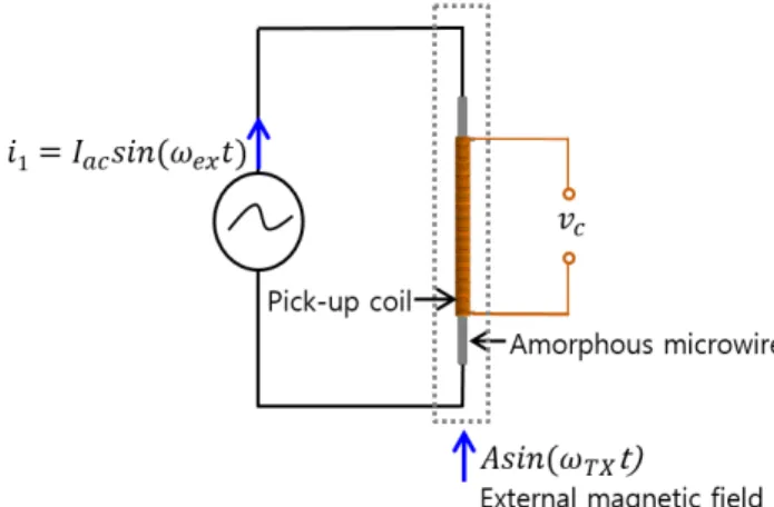
FIGURE 2. Schematic view of the voltage response in a classical off-diagonal giant magneto-impedance configuration.
literature [17]. The near-field region using the value of this skin depth, is defined as follows. If the transmission frequency range of 1-100 kHz in consideration of the communication environments, by definition, the near-field region is determined from several meters up to several kilometers depending on the composition of the in-organic materials in underground and underwater medium environments. For instance, the results of the calculation for the near-field region are as follows. In the granite material, the calculated value is 6.3 km at 1 kHz and 700 m at 100 kHz in the underground medium. In the underwater medium, the calculated value of the seawater is 100 m at 1 kHz and 10 m at 100 kHz. In addition, the calculated value for the natural water is 1 km at 1 kHz and 100 m at 100 kHz. Therefore, the magnetic field communication takes place in short-range coupling in the near-field region. Our research team aims to communicate underground and underwater magnetic field within a near-field region of up to 300 m using a giant magneto-impedance (GMI) sensor as the receiving element by selecting the transmission frequency according to the conditions of the underground and underwater medium conditions. The MI method has an inherent restriction because of a high path loss of 60 dB per decade at short distances. To solve this problem, AMR sensors have been proposed as replacements for conventional MI communication systems [11].
The advances in nano-thin film technology have enabled the development of GMR sensors, which exceed the sensitivity of AMR sensors. However, these sensors are less sensitive than GMI sensors, which are the focus of this study. The sensitivity of a typical GMI sensor can be as much as 500 times that of a GMR sensor [18].
Large impedance variations in CoFeSiB-based soft amorphous wires, which are called “the GMI effect,” were reported by Panina and Mohri in 1994 [19], [20]. The results on the GMI sensor and “the GMI effect” are currently being examined by several groups [21]–[23]. The proposed GMI sensors have the advantage of being easier to implement, less expensive, smaller, and higher performing than the GMI magnetometers being studied by the groups mentioned above. A previous study [24] proposed the use of a high-frequency magnetic probe with a 1 mm-thick glass substrate and a GMI sensor element for measuring EM radiation in a circuit.
Another study [25] proposed an off-diagonal GMI sensor that uses software-defined radio. This research provides an implementation concept of digital and real-time electronic devices for GMI sensors in an off-diagonal configuration. Although these studies focus on measuring only the magnetic field strength, the reported physical principles and outline models of the GMI effect demonstrate the potential for the use of magnetic communication in underground and underwater environments.
Fig. 1 shows the conceptual block diagram of receiver systems using a GMI sensor in magnetic communication.
The diagram corresponding to the GMI sensor shows an antenna and a mixer. The GMI effect is the impedance variation of the magnetic material used as an element for amplifying small signal variations in an external magnetic field. To extract messages from external magnetic signals, the appropriate demodulation and signal processing units are connected to the back end of the GMI sensor stage. Given that high sensitivity is the most notable characteristic of GMI sensors, a receiver system design based on the GMI effect enables high-performance magnetic communication.
This paper aims to provide a comprehensive analysis of the GMI sensor used as a radio frequency (RF) front end module corresponding to the preceding stage of de-modulation units in a receiver system for magnetic communication. The main characteristics for determining whether a radio receiver is well designed for a given purpose are gain, dynamic range, and noise spectral density. Specifically, when using the GMI sensor as a component of the receiver, the gain mentioned above means a voltage conversion ratio of magnetometers. These characteristics are analyzed by measuring two fabricated test GMI sensors. From this analysis, the bandwidth and channel capacity of these sensors are characterized. In addition, the equivalent magnetic noise spectral density, which dominantly affects the minimum signal level measurable in the magnetic communication channel, is analyzed in the frequency domain.
The remainder of this paper is structured as follows: Section II presents the theoretical background. An off-diagonal GMI sensor can be considered the same as the combination of an antenna and a mixer of the main components in a receiver system. It also explains the important physical characteristics of the GMI sensor. Section III describes the design of the proposed GMI sensors. Section IV gives the measurement strategies and experimental evaluation results, including the device characteristics. The concluding remarks and future work proposals are provided in Section V.
II. THEORETICAL BACKGROUND
This section explains the theoretical background. The off-diagonal GMI sensor can be considered the same as the combination of an antenna and a mixer of the main components in a receiver system (Fig. 1). It also describes the important physical characteristics of the GMI sensor (Fig. 2). As illustrated in Fig. 2, the sensing element consists of a pickup coil wound around an amorphous ferromagnetic microwire. The operation of an amorphous microwire at a high frequency, MHz, generates an induced voltage in the pickup coil. Here, as the number of turns of the pickup coil increases, the intrinsic sensor sensitivity (which corresponds to the off-diagonal term ( ) /
21
Z B B
∂ ∂
)
increases, and the excitation frequency tends to decrease [26]. The parasitic capacitance occurs according to the
number of turns of the pickup coil. As the number of turns of the pickup coil increases, the parasitic capacitance value decreases [26], [27]. As a result, the parasitic capacitance must be reduced to increase the intrinsic sensor sensitivity of the GMI sensor, and increasing the number of turns of the pickup coil is advantageous for increasing the intrinsic sensor sensitivity. However, as the excitation frequency is lowered, the number of turns of the pickup coil must be determined in consideration of the frequency of the external alternating current (AC) magnetic field to be sensed. The determined number of turns of the pickup coil is shown in Section III.
The induced voltage is proportional to the off-diagonal term Z21 of the impedance matrix of the two-port network sensing element, and this term Z21 is relatively less affected by the parasitic capacitance than the term Z22. Moreover, this induced voltage depends on the frequency and strength of the external magnetic field [26], [28]. For excitation, the angular frequency applied to the amorphous microwire for GMI is
ex
ω , the excitation current amplitude is Iac, the static field (bias field) is B0, and the induced voltage in the pickup coil can be expressed as
0 21 21 0 ( ) ( ) ( ) sin( ) c ac ex B B Z B v Z B b t I t B = ω ∂ = + ⋅ ⋅ ⋅ ∂ . (1)
Eq. (1), which is related to the AC component, shows a classic amplitude modulation. The key to Eq. (1) is the detection of the small signal b(t), and it is important for the differential term of Z21 for amplifying b(t). When the angular frequency of the external magnetic field is ωTX ,
( ) sin( TX )
b t = A ω t , and Eq. (1) can be written as
}
{
0 21 1 ( ) sin( ) 2 sin( ) sin( ) c ex ac B B ex TX ex TX Z B A v c t I B t t ω ω ω ω ω = ∂ = ⋅ + ⋅ ⋅ ∂ ⋅ + + − , (2)where c1 and A are arbitrary constants. The output
voltagevc has the three frequency components of the
ex
ω ,
TX
ex
ω ±ω . The output voltage of the GMI sensor is shown as the combination of an antenna and a mixer (Fig. 1). To extract the frequency component corresponding to ωTX from the three frequency components, a demodulation process is required. First, the two frequency components with
ex
ω ,
TX
ex
ω +ω are extracted from the three frequency components using the band pass filter that passes only the frequency components above
ex
ω in this demodulation stage. Second, it uses a frequency mixer. A local frequency corresponding to the excitation frequency of the GMI sensor is fed to the frequency mixer from an external oscillator, as shown in Fig. 1. Therefore, this local frequency and ωTX frequency cancel each other in the frequency mixer, and only the ωTX frequency component is extracted. After this demodulation stage, the output voltage
vc can be written as
0 21( ) ( ) c ac B B Z B v G I b t B = ∂ = ⋅ ⋅ ⋅ ∂
,
(3)where G is the gain associated with the demodulation stage. Through Eq. (3), the voltage conversion ratio corresponding to the small-signal gain can be defined as
(a) (b)
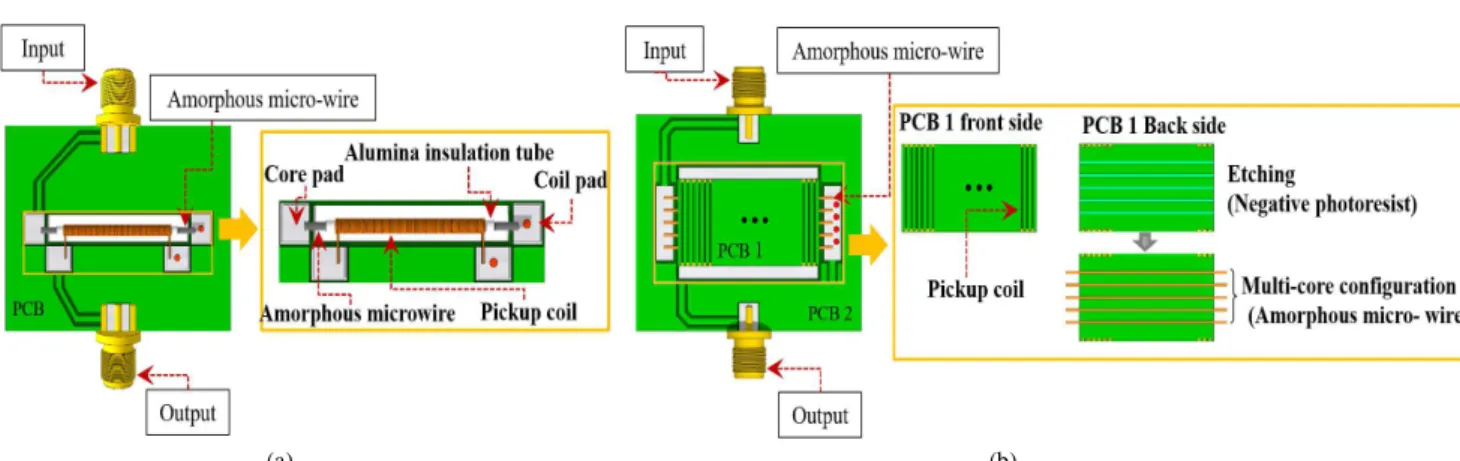
Figure 3. Schematic view of the proposed giant magneto-impedance (GMI) sensors: (a) Type A GMI sensor. (b) Type B GMI sensor.
TABLE I. Design parameters of GMI sensors
Type GMI wire diameter GMI wire length Number of turns of the pickup coil Number of core Overall PCB Size A 100 μm 30 mm 250 1 40 × 30 × 2 mm3 B 100 μm 30 mm 27 5 40 × 35 × 1.8 mm3
0 21( ) 1 c v ac B B v Z B S I b G B = ∂ ∂ = = ⋅ ∂ ∂ , (4) where ( ) / 21 Z B B
∂ ∂ is the intrinsic sensor sensitivity. The ability to obtain a large value is important for amplifying the small signal. In addition, intrinsic sensor sensitivity should be highly linear because it depends on the frequency and strength of the external magnetic field. The equivalent magnetic noise spectral density bn is obtained as the ratio between the output voltage noise spectral density en and the voltage conversion ratio Sv. It can be written as
n n v e b S = . (5) The units of the equivalent magnetic noise spectral density are T/√Hz.
Bandwidth, an area in the spectrum, is necessary for transmitting information signals centered on the frequency of the carrier signal. The following formula is applied to calculate the bandwidth of the proposed GMI sensors. According to Shannon’s channel capacity [29], it can be expressed as 2 log 1 S C BW N = × + , (6) where Cis the channel capacity, i.e., the bit transfer rate, and the unit is bit per second (bps). BW refers to the bandwidth, which is generally based on 3 dB. The units are expressed in hertz (Hz). S/Nis the signal-to-noise power ratio.
III. DESIGN OF A GMI SENSOR
Fig. 3 shows the structure of the two GMI sensor designs. The two types of GMI sensors use a soft magnetic material composed of a CoFeSiB amorphous microwire with a diameter of 100 µm and length of 30 mm. They use a structure in which the amorphous microwire is commonly embedded on a printed circuit board (PCB) substrate. The difference between the two types of sensors is the pickup coil pattern.
As shown in Fig. 3(a), the first type of GMI sensor, Type A, is directly wound around the solenoid-shaped pickup coil onto an alumina insulation tube inserted with an amorphous microwire, and the pickup coil is composed of a primary coil. The number of turns for the pickup coil was 250 with a single layer. A copper wire with a 0.1 mm diameter was used. The alumina insulation tube has an outer diameter of 0.8 mm, inner diameter of 0.4 mm, and length of 26 mm. The reason for using an alumina insulation tube is the difficulty in precisely winding the coil directly around the amorphous microwire without breaking the microwire. Therefore, the pickup coil can be effectively wound using an alumina insulation tube. Both ends of the amorphous microwire that are inserted into the alumina insulation tube are connected by being mounted on the core pad of the PCB substrate after silver plating treatment. The
pickup coil is connected to the coil pad by soldering. In the second type of GMI sensor, Type B, the pickup coil is patterned without winding the coil. Specifically, the PCB 1 structure of this sensor has a new geometry. The pickup coil is patterned on the front side of the PCB 1, which has negative etching with 110 µm-deep grooves in a straight line on the back side. On the back of PCB 1 are five parallel negative types of grooves in which the five amorphous microwires are inserted. Thus, this type has a multi-core configuration.
The composition of the multiple amorphous microwires allows for increases in the voltage conversion ratio of the GMI sensor. The proposed structure of Fig. 3(b) has the advantage of facilitating the formation of 1–5 amorphous microwires. The PCB 1 substrate is mounted with the PCB 2 substrate, and the patterned pickup coils on the PCB 2 substrate (omitted from Fig. 3[b]) and the front surface of the PCB 1 substrate are connected by soldering. The
(a)
(b)
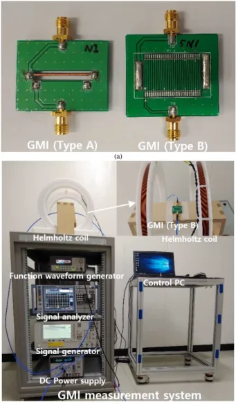
Figure 4.Experimental environment configuration of the proposed giant magneto-impedance (GMI) sensors: (a) Fabricated GMI sensors. (b) GMI measurement system.
number of turns for the pickup coil in the Type B GMI sensor is 27 with a single layer, and the pickup coil is composed of a primary coil. The five amorphous microwires are connected by being mounted on the core pad (omitted from Fig. 3[b]) of the PCB substrate after silver plating treatment (Fig. 3[a]). The Type B GMI sensor can be easily implemented with two PCB substrates. The design parameters of the proposed GMI sensors are
presented in Table I.
IV. RESULTS AND DISSCUSSIONS
A. EXPERIMENTAL SETUP AND CONFIGURATION
The designed GMI sensors are fabricated, as shown in Fig. 4(a). For the experimental evaluation of the sensors, an experimental measurement environment (i.e., a GMI
(a)
(b)
(c)
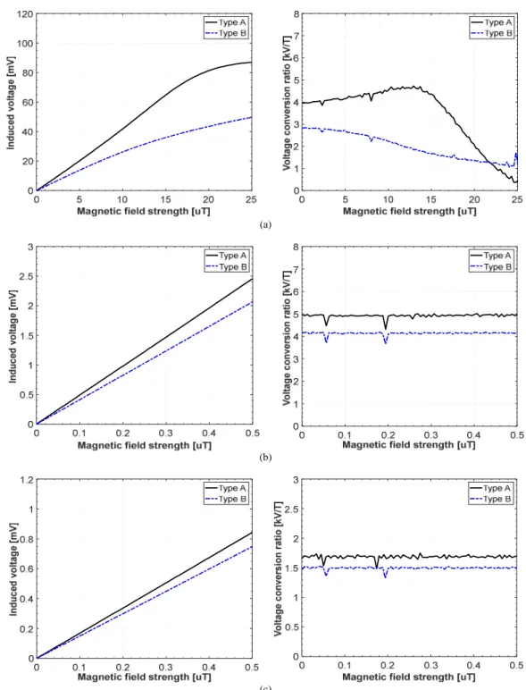
Figure 5.Comparison of the induced voltage (left) and voltage conversion ratios (right) of the two types of giant magneto-impedance sensors for (a) 1 kHz (Type A and Type B). (b) 30 kHz (Type A and Type B). (c) 100 kHz (Type A and Type B).
measurement system) is configured (Fig. 4).
The characteristics of the sensing elements, such as the AC magnetic field response, voltage noise spectral density, and equivalent magnetic noise spectral density, are assessed by the GMI measurement system.
For the external AC magnetic field, three candidate frequencies, namely 1 kHz, 30 kHz and 100 kHz, are selected to verify their applicability for underwater and underground magnetic field communication within the frequency range of 100 kHz in the near-field region. As shown in Fig. 4, the fabricated Helmholtz coil is used as a transmitting antenna. The signal input of the external AC magnetic field is supplied from the function waveform generator (Keysight, 33250A) to the Helmholtz coil. The Helmholtz coil transmits an external AC magnetic field to the GMI sensor in the form of a sine wave, which is a continuous wave. To receive an external AC magnetic field, input conditions to the GMI sensor are required to drive the GMI sensor. The input conditions of the GMI sensor can be set by setting the excitation frequency and the excitation voltage with AC voltage and direct current (DC) bias. The excitation parameters and bias condition corresponding to these input conditions affect the equivalent magnetic noise of an off-diagonal GMI sensor, and the equivalent magnetic noise varies according to these conditions. The DC bias current can decrease the equivalent magnetic sensor noise level in the white noise region because of the magnetic domain wall movement of the amorphous microwire [30]. The input for the excitation frequency and the AC voltage input of the excitation voltage for Type A and Type B GMI sensors is fed from thesignal generator (Keysight, E8257D), and the DC bias input of the excitation voltage is supplied from the DC power supply (Keysight, E3613A). The signal analyzer (Rohde & Schwarz, FSV4) is used to collect the output data of the sensor. The GMI measurement system is operated through a control personal computer (PC).
To validate the possibility of using GMI sensors in magnetic field communication, the Helmholtz coil is used to measure the bandwidth of the sensors under the external AC magnetic field of 0.001–100 kHz. The bit transfer rate is calculated through the analysis of the results. The detailed analysis is presented in sub-section E of section IV. The AC magnetic field response is measured for the operation of the Type A fabricated sensor at an excitation frequency of 20 MHz and Type B at an excitation frequency of 3 MHz. The difference in the excitation frequencies for the two sensors is the result of the intrinsic sensor sensitivity characteristics ( ( ) / ( )
21
Z B Z B
∂ ∂ ) of Eq. (1). In other words, the excitation frequency changes because of the difference in the number of pickup coil turns and the configuration of the multicore. Thus, the GMI sensors have different excitation frequencies.
The Type A sensor uses an excitation voltage of 3.3 Vpp and a DC bias of 50 mVdc.The Type B sensor uses an
excitation voltage of 3.3Vpp. The external frequencies used for the Helmholtz coil are 1, 30, and 100 kHz, which are the candidate frequencies for magnetic field communication. As the applied voltage to the Helmholtz coil, voltage change from 0.001 V to 10 Vpp is used, and this indicates a change in the magnetic field strength of the Helmholtz coil.
B. DYNAMIC RANGE AND VOLTAGE CONVERSION
RATIO
The induced voltage (vc) with a unit of mV, which represents the dynamic range for the GMI sensors, and the voltage conversion ratio (Sv) with a unit of kV/T are shown
(a)
(b)
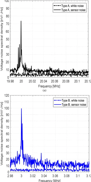
Figure 6.Voltage noise spectral density: (a) Type A giant magneto-impedance (GMI) sensor. (b) Type B GMI sensor.
in Fig. 5.
Fig. 5(a) shows the induced voltage and voltage conversion ratios for the GMI sensors under an external frequency of 1 kHz. When the Helmholtz coil operates at 1 kHz, the Helmholtz coil has an impedance |Z| of 73.77 Ω. An induced voltage of up to 87.1 mV and a voltage conversion ratio of 0.19 kV/T to 4.65 kV/T are achieved for Type A. For Type B, the induced voltage is 50.7 mV, and the voltage conversion ratio is 1 kV/T to 2.8 kV/T. The results confirm that the output linearity characteristics of
the GMI sensors at an external frequency of 1 kHz are not guaranteed and that the voltage conversion ratio value changes with the strength of the Helmholtz coil.
The induced voltage and voltage conversion ratio under an external frequency of 30 kHz are shown in Fig. 5(b). The Helmholtz coil has an impedance |Z| of 3.05 kΩ at 30 kHz. The two types of GMI sensors are guaranteed high linearity characteristics for the induced voltage. The achieved induced voltage and voltage conversion ratios are 2.5 mV and 4.95 kV/T for Type A and 2.1 mV and 4.15 kV/T for Type B, respectively.
(a)
(b)
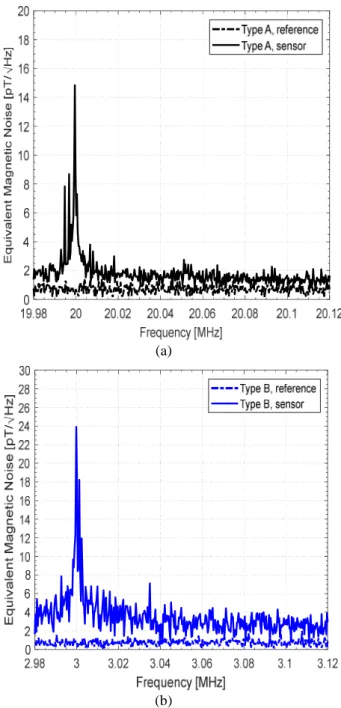
Figure 7. Equivalent magnetic noise spectral density: (a) Giant magneto-impedance (GMI) sensor Type A with the applied voltage conversion ratio of 4.95 kV/T. (b) GMI sensor Type B with the applied voltage conversion ratio of 4.15 kV/T.
(a)
(b)
Figure 8. Bandwidth: (a) Giant magneto-impedance (GMI) sensor with Type A. (b) GMI sensor with Type B.
The induced voltage and voltage sensitivity under the external frequency of 100 kHz using a Helmholtz coil are shown in Fig. 5(c). The Helmholtz coil has an impedance |Z| of 3.40 kΩ at 100 kHz. The achieved induced voltage and voltage conversion ratios are 0.84 mV and 1.7 kV/T for Type A and 0.74 mV and 1.67 kV/T for Type B, respectively.
These results confirm that the induced voltage has linear characteristics. However, the induced voltage and voltage conversion ratios are lower than those in Fig. 5(b).
Regarding the applicability of magnetic field communication, the results shown in Fig. 5 confirm that among the three external frequencies (1, 30, and 100 kHz), 30 kHz provides the best performance characteristics for the induced voltage and voltage conversion ratios. In addition, Type A exhibits better performance characteristics than Type B. Therefore, Type B does not perform as well as Type A. The reason is the difference in the number of turns for the pickup coils in the GMI sensors. The number of turns for the Type B pickup coil is 9.3 times less than that for the Type A pickup coil.
C. VOLTAGE NOISE SPECTRAL DENSITY
Fig. 6 shows the voltage noise spectral density (en) results for the GMI sensors. The excitation conditions are the same as those in the AC magnetic field response. The excitation frequencies of the GMI sensors and the external magnetic field of a frequency range of 1–100 kHz for magnetic field communication are considered in the noise level measurements. Thus, the considered frequency bandwidth for the noise level is 19.98–20.12 MHz for Type A and 2.98–3.12 MHz for Type B.
Figs. 6(a) and (b) show the voltage noise spectral density for Type A and Type B. The measured average white noise for Types A and B are the same. The value is 3.5 nV/√Hz. The average noise levels of approximately 10 nV/√Hz and 15 nV/√Hz are achieved for Type A and Type B, respectively. The exception is the excitation frequency
region in the considered frequency range. Specifically, for an external frequency of 30 kHz, the noise levels of approximately 7.4 nV/√Hz at 20.03 MHz and 12.3 nV/√Hz at 3.03 MHz are achieved for Type A and Type B,
respectively.
In both results, the noise levels are measured at high frequencies in the MHz region; thus, the flicker noise 1/f is very small. Large noise values are found at the excitation frequencies for the two types of GMI sensors. Both sensors appear to have excellent noise characteristics of tens of nV/√Hz levels. However, the Type A GMI sensor seems to have better noise characteristics than Type B.
D. EQUIVALENT MAGNETIC NOISE SPECTRAL DENSITY
Fig. 7 shows the results of the equivalent magnetic noise spectral density for the two types of GMI sensors. The equivalent magnetic noise spectral density bn can be obtained with Eq. (5). For an external frequency of 30 kHz, the considered voltage conversion ratio for Type A and Type B is approximately 4.95 kV/T of 20.03 MHz and 4.15 kV/T of 3.03MHz, respectively. For the voltage noise spectral density en , the results in Fig. 6 are applied.
The results of the equivalent magnetic noise spectral density for Type A and Type B are shown in Figs. 7(a) and (b). The calculated average equivalent magnetic noise of 2 pT/√Hz and 3.7 pT/√Hz is achieved for Type A and Type B, respectively. The exception is the excitation frequency region in the considered frequency bandwidth. In Fig. 7, the dash-dotted lines for Type A and Type B refer to the noise reflected by the white noise in Fig. 6 and the voltage TABLE II. Bandwidth characteristics of giant magneto-impedance sensors
External frequency 3dB Bandwidth (Type A) Channel capacity (Type A) 3dB Bandwidth (Type B) Channel capacity (Type B) 1 kHz 0.49 kHz 16 kbps 0.6kHz 17 kbps 10 kHz 3 kHz 75 kbps 3.3 kHz 72 kbps 30 kHz 10.3 kHz 222 kbps 12.7 kHz 240 kbps 50 kHz 17 kHz 339 kbps 21.5 kHz 379 kbps 70 kHz 20 kHz 385 kbps 26.4 kHz 447 kbps 90 kHz 26.7 kHz 497 kbps 34.2 kHz 557 kbps
TABLE III. Summary of the performance of giant magneto-impedance sensors
Parameter Type A Type B
Dynamic range Max. 2.5 mVa Max. 2.1 mVa
Voltage conversion
ratio 4.95 kV/T
a
4.15 kV/Ta
Average white noise 3.5 nV/√Hz 3.5 nV/√Hz
Average sensor noise 10 nV/√Hz 15 nV/ Hz Sensor noise 7.4 nV/√Hza 12.3 nV/√Hza Average equivalent noise 2 pT/√Hz b 3.7 pT/√Hzb
Equivalent noise 1.5 pT/√Hza,b 3 pT/√Hza,b
Bandwidth (3 dB) 10.3 kHza 12. 7kHza
Channel capacity
(bit transfer rate) 212 kbps
a
240 kbpsa a
Relative comparisons of the performance of Type A at 20.03 MHz and Type B at 3.03 MHz.
b
Relative comparison of the voltage conversion ratios of 4.95kV/T at 20.03 MHz for Type A and 4.15 kV/T at 3.03 MHz for Type B.
communication (see Fig. 8 for results). The bandwidths of the GMI sensors are measured by fixing the voltage of the Helmholtz coil to 3Vpp and varying its external frequency from 0.001 kHz to 100 kHz. The bandwidth and channel capacity results are summarized in Table II.
Fig. 8(a) shows the measured bandwidth for Type A. A 3 dB bandwidth of approximately 10.3 kHz at a center frequency of 20.03 MHz is obtained. The channel capacity, i.e., the bit transfer rate, for Type A is calculated with Eq. (6). The calculated channel capacity is 222 kbps when the measured signal-to-noise power ratio value is approximately 65 dB.
The measured bandwidth of Type B is shown in Fig. 8(b). A 3 dB bandwidth of approximately 12.7 kHz at a center frequency of 3.03 MHz is achieved. The channel capacity for Type B is calculated at 240 kbps when the measured signal-to-noise power ratio value is 57 dB.
The bandwidths for the two types of GMI sensors increase as the external frequency increases. The bandwidth and channel capacity results for Type B are better characteristics than those for Type A. In addition, considering only the bandwidth and channel capacity characteristics facilitates the selection of an external frequency corresponding to a high frequency of almost 100 kHz. However, the results, as illustrated in Fig. 5, indicate that the best voltage conversion ratio is obtained with the 30 kHz external frequency rather than the 1 and 100 kHz frequencies. The measured bandwidth and channel capacity at 30 kHz are reasonably acceptable. Therefore, the selection of an external frequency of 30 kHz is deemed appropriate.
Moreover, given the overall device characteristics of the sensor and bandwidth characteristics for Type A and Type B, Type A is a sensor with excellent characteristics and may be used as a test sensor for application in magnetic field communication. Conversely, Type B has better bandwidth characteristics than Type A. Type B achieves excellent equivalent noise spectral density characteristics of pT/√Hz levels similar to Type A. Type B has advantages in terms of mass production and manufacturing process compared with Type A. Therefore, Type B can also be a test sensor for application in magnetic field communication. This study confirms the possibility of using the proposed GMI sensors as audio receivers in magnetic field
evaluation of the proposed GMI sensors. These results indicate that a weak magnetic field can be received in magnetic field communication in the near-field region. When an external frequency of 30 kHz is used, the bandwidth and channel capacity are found to be suitable for the use of GMI sensors in magnetic field communication. As a result, the possibility of applying the proposed GMI sensors to a receiving element for magnetic field communication, which is a new application field, can be confirmed. Studies on modulation and demodulation methods (e.g., frequency shift keying and the phase shift keying) and transmission methods (e.g., synchronous and asynchronous methods) as communication methods for magnetic field communication will be conducted in future studies. Moreover, a demodulation circuit of a GMI receiver using a GMI sensor, which performs an experimental evaluation of the GMI receiver, will be designed and implemented.
ACKNOWLEDGMENT
This work was supported by the Institute of Information & Communications Technology Planning & Evaluation(IITP) grant funded by the Korea government(MSIT) (No.2019-0-00007, Magnetic Field Communication Technology Based on 10pT Class Magnetic Field for Middle and Long Range).
REFERENCES
[1] Z. Sun and I. F. Akyildiz, “Underground wireless communication using magnetic induction,” Proc. 2009 IEEE ICC, 2009.
[2] S. Wang and Y. Shin, “Efficient routing protocol based on reinforcement learning for magnetic induction underwater sensor networks,” IEEE Access, vol. 7, pp. 82027–82037, 2019.
[3] P. Ripka, Magnetic Sensors and Magnetometers, Norwood, MA, USA: Artech House, 2001.
[4] M. Phan and H. Peng, “Giant magnetoimpedance materials: Fundmen-tals and applications,” Progr. Mater. Sci., vol. 53, no. 2, pp. 323–420, Feb. 2008.
[5] T. Dogaru and S. T. Smith, “Giant magnetoresistance-based eddy-current sensor,” IEEE Trans. Magn., vol. 35, no. 5, pp. 3831–3838, Sep. 2001.
[6] P. Ripka, M. Janosek, and M. Butta, “Crossfield sensitivity in AMR sensors,” IEEE Trans. Magn., vol. 45, no. 10, pp. 4514–4517, Sep. 2009.
[7] L. Ejsing, M. F. Hansen, and A. Menon, “Magnetic microbead detection using the planar Hall effect,” J. of Magnet. Magn. Mater., vol. 293, no. 1, pp. 677–684, May 2005.
[8] S. Oh, B. J. Jang, and H. Chae, “Sensitivity enhancement of a vertical-type CMOS Hall device for a magnetic sensor,” J. Electromagn. Eng. Sci., vol. 18, no. 1, pp. 35–40, Jan. 2018. [9] J. Wang, B. Zhou, X. Liu W, Wu, L. Chen, B. Han, and J. Fang, “An
improved target-field method for the design of uniform magnetic field coils in miniature atomic sensors,” IEEE Access, vol. 7, pp. 74800–74810, 2019.
[10] P. H. Hsieh and S. J. Chen, “Multilayered vectorial fluxgate magnetometer based on PCB technology and dispensing process,”
Mea. Sci. Technol., vol. 30, no. 12, p. 125101. 2019.
[11] M. Hott, P. A. Hoeher, and S. F. Reinecke, “Magnetic communication using high-sensitivity magnetic field detectors,” Sensors, vol. 19, no. 15, p. 3415, Aug. 2019.
[12] Z. Wang, X. Wang, M. Li, Y. Gao, Z. Hu, T. Nan, X. Laing, H. Chen, J. Yang, S. Cash, and N. X. Sun, “Highly sensitive flexible magnetic sensor based on anisotropic magnetoresistance effect,” Adv. Mater., vol. 28, no. 42, pp. 9370–9377, 2016.
[13] L. Rong, S. Bao, J. Wu, G. Zhang, L. Qiu, S. Zhang, Y. Wang, H, Dong, Y. Pei, and X. Xie, “High-performance dual-channel squid-based TEM System and its application,” IEEE Trans. Appl. Supercond., vol. 29, no. 8, pp. 1-4, Dec. 2019.
[14] S. J. Lee, K. Jeong, J. H. Shim, H. J. Lee, S. Min, H. Chae, S. K. Namgoong, and K. Kim, “SQUID-based ultralow-field MRI of a hyperpolarized material using signal amplification by reversible exchange,” Sci. Rep. vol. 9, no. 1 pp. 1-8, 2019.
[15] V. Gerginov, F. C. S. da Silva, and D. Howe, “Prospects for magnetic field communications and location using quantum sensors,”
Rev. Sci. Instrum., vol. 88, no. 12, p. 125005, 2017.
[16] Y. Kim, S. Boo, G. Kim, N. Kim, and B. Lee, “Wireless power transfer efficiency formula applicable in near and far fields,” J. Electromagn. Eng. Sci., vol. 19, no. 4, pp. 239–244, Oct. 2019. [17] T. E. Abrudan, O. Kypris, N. Trigoni and A. Markham, "Impact of
rocks and minerals on underground magneto-inductive communication and localization", IEEE Access, vol. 4, pp. 3999-4010, 2016.
[18] H. X. Peng, F. Qin, and M. H. Phan, Ferromagnetic Microwire Composites: From Sensors to Microwave Applications, Cham, Switzerland: Springer, 2016.
[19] L. V. Panina, K. Mohri, “Magneto-impedance effect in amorphous wires,” Appl. Phys. Lett., vol, 65, no. 9, pp. 1189–1191, Jun. 1994. [20] L.V. Panina, K. Mohri, T. Uchiyama, M. Noda, and K. Bushida,
“Giant magneto-impedance in co-rich amorphous wires and films,”
IEEE Trans. Magn., vol. 31, no. 2, pp. 1249–1260, Mar. 1995. [21] M. Malátek and L. Kraus, “Off-diagonal GMI sensor with
stress-annealed amorphous ribbon,” Sens. Actuators A: Phys., vol. 164, no. 1, pp. 41–45, 2010.
[22] F. Jin, J. Wang, L. Zhu, W. Mo, K. Dong and J. Song, “Impact of adjustment of the static working point on the 1/f noise in a negative feedback GMI magnetic sensor,” IEEE Sensors J., vol. 19, no. 20, pp. 9172–9177, 15 Oct. 2019.
[23] J. Chen, J. Li, and L. Xu, “Highly integrated MEMS magnetic sensor based on GMI effect of amorphous wire,” Micromachines vol. 10, pp. 237, Apr. 2019.
[24] K. Tan, K. Yamakawa, T. Komakine, M. Yamaguchi, Y. Kayano, and H. Inoue, “Detection of wide band signal by a high frequency carrier-type magnetic probe,” J. Appl. Phys., vol. 99 no. 8, pp. 08B315, Apr. 2006.
[25] A. Asfour, J. P. Yonnet, and M, Zidi, “Toward a novel digital electronic conditioning for the GMI magnetic sensors: The software defined radio,” IEEE Trans. Magn., vol. 51 no. 1, pp. 1–4, Feb. 2015. [26] B. Dufay, S. Saez, C. P. Dolabdjian, A. Yelon, and D. Ménard, “Characterization of an optimized off-diagonal GMI-based magnetometer,” IEEESensors J., vol. 13, no. 1, pp. 379–388, Jan. 2013.
[27] K. L. Corum and J. F. Corum, “RF coils helical resonators and voltage magnification by coherent spatial modes,” IEEE Microw. Rev., vol. 7, no. 2, pp. 36–45, Sep. 2001.
[28] E. Portalier, B. Dufay, S. Saez, and C. Dolabdjian, “Noise behavior of high-sensitive GMI-based magnetometer relative to conditioning parameters,” IEEE Trans. Magn., vol. 51, no. 1, pp. 1–4, Jan. 2015. [29] S. Aslam, N. U. Hasan, J. W. Jang, and K. G. Lee, “Optimized
energy harvesting, cluster-head selection and channel allocation for IoTs in smart cities,” Sensors, vol. 16, no. 12, p. 2046, Dec. 2006. [30] E. Paperno, “Suppression of magnetic noise in the
fundamental-mode orthogonal fluxgate,” Sens. Actuators A, Phys., vol. 116, no. 3, pp. 405–409. Oct. 2004.
JANG-YEOL KIM received his B.S., M.S., and Ph.D. degrees in information and communication engineering from Chungbuk National University, Cheongju, Republic of Korea, in 2010, 2012, and 2017, respectively. Since 2012, he has been with the Electronics Telecommunications Research Institute, Daejeon, Republic of Korea. His research interests include antenna design, thermal therapy algorithms, microwave sensing, and electromagnetic sensors.
IN-GUI CHO received his B.S. and M.S. degrees from the Department of Electronic Engineering, Kyungpook National University, Daegu, South Korea, in 1997 and 1999, respectively, and his Ph.D. degree in electrical engineering from the Korea Advanced Institute of Science and Technology, Daejeon, South Korea, in 2007. Since May 1999, he has been with the Electronics and Telecommunications Research Institute, Daejeon, South Korea, where he has designed and developed optical backplane, optical chip-to-chip interconnect system, and magnetic resonance wireless power transfer. His current research interests include simulation and development of WPT components, such as planar magnetic resonators and magnetic resonators for three-dimensional WPT.
HYUN JOON LEE received his B.S., M.S., and Ph.D. degrees from the Department of Physics, Pusan National University, Busan, South Korea, in 2008, 2011, and 2018, respectively. Between 2018 and 2019, he was a postdoctoral associate at the Korea Research Institute of Standards and Science working on optical magnetometry. Since 2019, he has been with the Electronics and Telecommunications Research Institute, Daejeon, Korea. His research interests include ultra-low field magnetic resonance and the development of highly sensitive quantum sensors.
JAEWOO LEE received his B.S. degree in electrical and electronics engineering from Korea University, Seoul, Republic of Korea, in 2000, his M.S. degree in information and communication engineering from Gwangju Institute of Science and Technology (GIST), Gwangju, Republic of Korea, in 2002, and his Ph.D. in electrical engineering from Korea Advanced Institute of Science and Technology Daejeon, Republic of Korea, in 2017. After graduate school (GIST) in 2002, he joined a micro-system team at the Electronics and Telecommunication Research Institute (ETRI), Daejeon, Korea. For three years, he focused on developing bridge-type RF MEMS switches using an Au membrane on a
antennas, broadband antennas, wireless power transmission, and RF energy harvesting.
SEONG-MIN KIM received his B.S., M.S., and Ph.D. degrees from the Department of Electronic Engineering, Kyungpook National University, Daegu, Korea, in 1997, 1999, and 2016, respectively. Since March 2001, he has been with the Electronics and Telecommunications Research Institute, Daejeon, Korea. He has developed RF systems for WiFi, mobile wimax, LTE, LTE-A, and WPT. His current research interests include the design and implementation of WPT systems, control algorithms for WPT, and network management for WPT systems.
SANG-WON KIM received his B.S. and M.S. degrees from the Department of Electronic Engineering, Sogang University, Seoul, Korea, in 1999 and 2002, respectively, and his Ph.D. degree from the Department of Radio and Information Communications Engineering from Chungnam National University, Daejeon, Korea, in 2018. Since 2005, he has been with the Electronics and Telecommunications Research Institute, Daejeon, Korea. He has developed RF systems for cognitive radio, direction finding, and WPT. His research interests include RF circuit design and WPT systems.
SEUNGYOUNG AHN received his B.S., M.S., and Ph.D. degrees from the Korea Advanced Institute of Science and Technology, Daejeon, South Korea, in 1998, 2000, and 2005, respectively, all in electrical engineering. From 2005 to 2009, he worked as a senior engineer at Samsung Electronics, Suwon, South Korea, where he was in charge of high-speed board design for laptop computer systems. He is currently an associate professor at Cho Chun Shik Graduate School of Green Transportation, Korea Advanced Institute of Science and Technology. His research interests include wireless power transfer system design and electromagnetic compatibility design for electric vehicles and high-performance digital systems.
KIBEOM KIM received his B.S. degree from Koreatech, Cheonan, South Korea, in 2011, and his M.S. and Ph.D. degrees from the Korea Advanced Institute of Science and Technology (KAIST), Daejeon, South Korea, in 2014 and 2019, respectively. He is currently a research assistant professor at Cho Chun Shik Graduate School of Green Transportation, KAIST. His current research interests include electromagnetic interference/electromagnetic compatibility for