A novel integrated laser, that is, a distributed reflector laser diode integrated with an electroabsorption modulator, is proposed to improve the output efficiency, single-mode stability, and chirp. The proposed laser can be realized using the selective metalorganic vapor phase epitaxy technique (that is, control of the width of the insulating mask), and its fabrication process is almost the same as the conventional electroabsorption modulated laser (EML) process except for the asymmetric coupling coefficient structure along the cavity. For our analysis, an accurate time-domain transfer-matrix-based laser model is developed. Based on this model, we perform steady-state and large-signal analyses. The performances of the proposed laser, such as the output power, extinction ratio, and chirp, are compared with those of the EML. Under 10-Gbps NRZ modulation, we can obtain a 30% higher output power and about 50% lower chirp than the conventional EML. In particular, the simulation results show that the chirp provided by the proposed laser can appear to have a longer wavelength side at the leading edge of the pulse and a shorter wavelength side at the falling edge.
Keywords: Distributed reflector laser diode, electroabsorption modulator, monolithic integration.
Manuscript received May 20, 2012; revised Oct. 2, 2012; accepted Oct. 30, 2012.
This work was supported by the “Energy Efficient Power Semiconductor Technology for Next Generation Data Center” IT R&D project (No. 10038766) of Korea Ministry of Knowledge Economy (MKE/KEIT).
Oh Kee Kwon (phone: +82 42 860 1366, [email protected]) and Yong Soon Beak ([email protected]) are with the Components & Materials Research Laboratory, ETRI, Daejeon, Rep. of Korea.
Yun C. Chung ([email protected]) is with the Department of Electrical Engineering, Korean Advanced Institute of Science and Technology, Daejeon, Rep. of Korea.
Hyung-Moo Park ([email protected]) is with the Department of Electrical Engineering, Dongguk University, Seoul, Rep. of Korea.
http://dx.doi.org/10.4218/etrij.13.0112.0305
I. Introduction
A directly modulated laser diode has been employed for most commercial fiber-optic transmission systems, such as those at 2.5 Gb/s. However, its modulation bandwidth and transmission distance are limited by the wavelength chirp of the signal source. To overcome these problems, one of the main candidates is the laser diode integrated with an external modulator [1]-[5]. Among such optical sources, particularly an electroabsorption modulated laser (EML), a distributed feedback laser diode (DFB-LD) monolithically integrated with an electroabsorption modulator (EA-MOD) utilizing the quantum confined Stark effect (QCSE) has generally been the preferred choice owing to its compactness, high reliability, and easy fabrication [2], [4], [5]. Multiple quantum wells (MQWs) in this integrated laser can be grown one at a time using the selective metalorganic vapor phase epitaxy (MOVPE)
technique [2], [5]. In addition, an optical coupling efficiency of almost 100% can be obtained between a DFB-LD and an EA-MOD.
For the use of this integrated laser diode in higher speed applications (such as >10 Gb/s), a clear eye opening with a small wavelength chirp under a large-signal modulation should be provided. However, an optical signal reflected from the output facet can perturb the lasing condition of a DFB-LD, which in turn causes unwanted power fluctuations and a large chirp of the output signal under modulation [4]-[7]. It was recently reported that this facet reflection can also cause a large peak or valley in the frequency response [5] and degrade the signal quality [6]. This problem is a critical issue for the design of a high-speed integrated laser diode since it frequently occurs in a laser diode integrated with a short EA-MOD. There are several chirp-reduction methods commonly used to avoid such
Proposal and Analysis of Distributed Reflector-Laser
Diode Integrated with an Electroabsorption Modulator
an influence on an integrated laser diode [5], [7]-[9]. For example, it was reported that this facet-reflection-induced chirp can be reduced by decreasing the reflectivity of the output facet to less than approximately 2×10⁻⁴ [7]. However, it is difficult to
decrease the reflectivity to such a low value without utilizing a window structure [8] or a tilted waveguide [5] or accurately control the thickness of the dielectric coating materials. This influence can also be alleviated by realizing DFB-LDs with high immunity to an external feedback (that is, high κL DFB-LD) [9]. However, in spite of its improvement in the reflection immunity, this method is still debatable since the use of high κL DFB-LDs can result in the reduction of output power and the degradation of single-mode stability owing to the longitudinal spatial hole burning (LSHB) [10]. On the other hand, from an operational point of view, it is well known that this influence can be suppressed by increasing the bias voltage of an EA-MOD. This is equivalent to a decrease in the detuning between the lasing wavelength of a DFB-LD and the absorption peak wavelength of an EA-MOD. In this case, however, the output power is reduced owing to the increase of the absorption of the EA-MOD.
To achieve high output power through the output facet, the high reflection (HR) films at the rear-facet of the DFB-LD and the anti-reflection films at the front-facet of the EA-MOD are coated. However, since a single-mode device yield of DFB-LD depends strongly on the grating phase at the HR-coated facet, we must evaluate its lasing properties one by one, which in turn substantially increases the manufacturing cost. To solve this problem, in this paper, we propose a distributed reflector laser diode (DR-LD) monolithically integrated with an EA-MOD, which can provide a high single-mode yield irrespective of the facet-grating phase, a high output efficiency, and a high insensitivity to residual facet reflection. In addition, the fabrication process of this proposed laser is almost the same as the conventional EML process except for an asymmetric coupling coefficient (ACC) structure, which can be realized by controlling the duty of the grating along the cavity [11], [12].
This paper is organized as follows. Section II describes the static and dynamic analyses for the monolithically integrated laser. A comparison between the conventional EML and proposed laser for the static and dynamic properties is described in section III. Finally, some concluding remarks regarding this proposal are given in section IV.
II. Proposal of DR-LD/EA-MOD and Theory behind
Analysis Model
1. Proposal of DR-LD/EA-MOD
Figure 1 shows schematic diagrams of the conventional
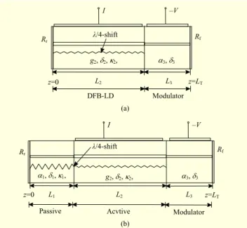
Fig. 1. Schematic diagrams of (a) DFB-LD/EA-MOD and (b) DR-LD/EA-MOD. I –V Rr Rf λ/4-shift L2 L3 z=LT z=0 DFB-LD Modulator g2, δ2, κ2, α3, δ3
Passive Acvtive Modulator
(a) λ/4-shift α1, δ1, κ1, g2, δ2, κ2, α3, δ3 z=0 L1 L2 L3 z=LT Rf I –V Rr (b)
EML, the DFB-LD/EA-MOD, and the proposed laser, the DR-LD/EA-MOD, respectively. The DR-LD/EA-MOD consists of a passive reflector (Region I), an active region (Region II), and an EA-MOD (Region III). To guarantee high single-mode stability along the optical cavity, the λ/4-shifted structure is selected. The phase-shift of the DR-LD is located between the passive reflector and the active region, whereas that of the DFB-LD is located in the center of the active region. In the proposed laser, the DR-LD can provide high output efficiency from the reflectivity of the passive reflector. In particular, the mode instability caused by the initial grating phase at the rear-facet can be removed (owing to the high reflectivity of the passive reflector), and, as a result, a high single-mode yield can be achieved. It was reported that the effective linewidth enhancement factor (αeff) in a DR-LD, which has an effect on
the linewidth and chirp of the output signal, can be lower than the material linewidth enhancement factor (αH) by properly
controlling the wavelength detuning between the active region and the passive reflector (that is, wavelength-dependent threshold gain) [13], [14]. In a previously reported structure, however, it was difficult to avoid the regrowth process when realizing a passive reflector. The selective MOVPE technique, a growth technique that can create an MQW on a substrate patterned using an insulating mask such as SiO2, has recently
become the core technology in the fabrication of integrated devices. This technique can be used to create various waveguide structures for only one growth by controlling the width of the insulating mask. From this perspective, the fabrication process of the DR-LD/EA-MOD is almost the same as that of the DFB-LD/EA-MOD, except for the ACC
structure along the cavity. 2. Analysis Model
To investigate the operational properties of the proposed laser theoretically, we develop a time-domain transfer-matrix-based laser model composed of various longitudinal regions. To consider the LSHB, we divide each region into small sections of length Δz and assume all variables in each section to be constant (although these variables can have different values from one section to another). In this model, we consider the changes of the absorption coefficient and refractive index of an EA-MOD as a function of the applied voltage and neglect the thermal effect, the noise characteristics, and the electrical parasitics including the RF property of an EA-MOD [15] and the bonding wire [16]. To verify the consistency of our model and understand the performance of the integrated lasers, the static and dynamic properties of a DR-LD/EA-MOD is compared with those of a conventional DFB-LD/EA-MOD.
The electric field in this integrated laser can be approximated by
(
)
0 0 0 0 ( , , , ) , ( , ) j z ( , ) j z j t, E t x y z =U x y R t z e⎡ −β +S t z e β ⎤eω ⎣ ⎦ (1)where U0(x, y) is the electric field of the guided mode, which
depends mainly on the waveguide structure, and R(t, z) and
S(t, z) are the time-dependent slowly varying forward and
backward propagating waves along the longitudinal direction z, respectively. In addition, β0 and ω0 are the propagation constant
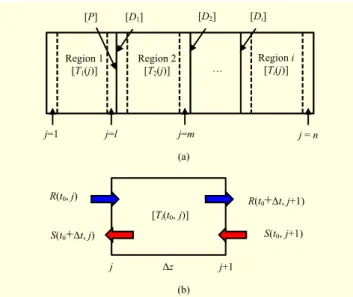
and the angular frequency in the Bragg condition, respectively. Figure 2 shows a schematic diagram of a time-domain transfer-matrix-based model and the relation between R(t, z) and S(t, z) within the section of Δz during the time interval of Δt. In this model, assuming that the medium remains unchanged over Δt, R(t, z) and S(t, z) from z = 0 to z = L at t0 and t0+Δt are
related by the transfer matrices expressed by
[
]
0 0 0 0 0 ( , ) ( , 0) ( , ) ( , ) ( , 0) R t t z L R t z T t L S t z L S t t z + Δ = = ⎡ ⎤ ⎡ ⎤ = ⎢ = ⎥ ⎢ + Δ = ⎥ ⎣ ⎦ ⎣ ⎦, (2)where [T(t0, L)] is the overall transfer matrix at t = t0. [T(t, L)]
can be written as follows:
[
]
[
3][ ]
2[
2][ ][ ] [
1 1]
1 1 1 ( , ) n ( , ) m ( , ) l ( , ) , j m j l j T t L T t j D T t j P D T t j = + = + = =∏
∏
∏
(3) where [Ti(t0, j)] is the transfer matrix of the j-th (j= 1, 2, ... , n)section of the i-th region at t = t0, and subscript i stands for the
passive reflector, active region, and EA-MOD when equal to 1, 2, and 3, respectively. In addition, [D] is a matrix representing the reflection induced by the refractive index difference between the regions, and [P] is the matrix representing the
Fig. 2. (a) Schematic diagram of transfer-matrix-based laser model and (b) relationship between R(t, z) and S(t, z) within section length of Δz during time interval of Δt. [Ti(t0, j)]is transfer matrix of j-th section of i-th region at
t = t0. … Region 1 [T1(j)] Region 2 [T2(j)] j = n [P] [D1] Region i [Ti(j)] [D2] [Di] j=1 j=l j=m (a) j Δz j+1 R(t0, j) S(t0+Δt, j) R(t0+Δt, j+1) S(t0, j+1) [Ti(t0, j)] (b)
phase shift. [Ti(t, j)] can be written as follows:
[
]
11 12 21 22 ( , ) ( , ) ( , ) ( , ) ( , ) i i i i i T t j T t j T t j T t j T t j ⎡ ⎤ = ⎢ ⎥ ⎣ ⎦, (4) where( )
(
)
( )
( )
( )
(
)
11 , , ( , ) cosh , sinh ( , ) , , i i i i i i t j j t j T t j t j z t j z t j α δ γ γ γ − = Δ + Δ (5-1)(
)
12( , ) sinh ( , ) , ( , ) j i i i i j T t j t j z e t j κ γ γ − Ω = − Δ (5-2)(
)
21( , ) sinh ( , ) , ( , ) j i i i i j T t j t j z e t j κ γ γ Ω = Δ (5-3)( )
(
)
( )
( )
( )
(
( )
)
22 , , ( , ) cosh , sinh , , , i i i i i i t j j t j T t j t j z t j z t j α δ γ γ γ − = Δ − Δ (5-4)( )
, 2(
( )
,( )
,)
2 2, i t j i t j j i t j γ = α − δ +κ (6)( )
, (( )
, absp( )
) / 2, i t j ig t j i i t α = Γ − − Γα α (7)( )
( )
eff ,( )
0 2 , , i t j t n i t j π δ β λ = − , (8) where αi(t, j) and δi(t, j) denote the amplitude gain anddetuning from the Bragg condition, respectively; κ and Ω are the coupling coefficient and initial grating phase of the grating
regions; Γi and αi are the optical confinement factor and optical
loss of each region; g(t, j) is the material gain of the active region; and αabsp(t) is the material absorption coefficient of an
EA-MOD. [Di] can be written as follows:
[ ]
eff , 1 eff , eff , 1 eff ,
eff, 1 eff , 1
eff, 1 eff , eff , 1 eff ,
eff , 1 eff , 1 ( 1) ( ) ( 1) ( ) 2 ( 1) 2 ( 1) . ( 1) ( ) ( 1) ( ) 2 ( 1) 2 ( 1) i i i i i i i i i i i i i n j n j n j n j n j n j D n j n j n j n j n j n j + + + + + + + + + + + − ⎡ ⎤ ⎢ + + ⎥ ⎢ ⎥ = ⎢ + − + + ⎥ ⎢ ⎥ + + ⎢ ⎥ ⎣ ⎦ (9)
When we know all spatial field distributions at t = t0, the field
distributions at t = t0+Δt can be obtained consecutively by
0 ,21 0 0 0 ,22 0 ( , 1) ( , ) ( , ) ( , ) ( , ) i i S t j T t j R t j S t t j T t j + − + Δ = (10) 0 ,11 0 0 ,12 0 0 ( , 1) i ( , ) ( , ) i ( , ) ( , ) R t + Δt j+ =T t j R t j +T t j S t + Δt j , (11) where R(t0+Δt, z = 0) and S(t0+Δt, z = L) can be obtained by the
boundary conditions: 0 0 ( , 0) L ( , 0), R t + Δt z= =r S t + Δt z= (12) 0 0 ( , ) R ( , ), S t + Δt z=L =r R t + Δt z=L (13)
where rL and rR are the reflection coefficient at z = 0 and z = L,
respectively. In a semiconductor laser, g(t, j) and neff,i(t, j) are
varied with the carrier density N(t, z), photon density Pd(t, z) (=
|R(t, z)|2+|S(t, z)|2), and a lasing wavelength of λ(t). They can be
modeled as follows:
(
)
( )
( )
( )
( )
2 0 0 1 0 2 0 , , ( , ) ( ( , )) , 1 , i p d g N S a N t z N a t a N t z N P t z λ λ λ ε ⎡ ⎤ − − ⎣ − − − ⎦ = + (14)( )
(
)
(
( )
)
( )
( )
( )
eff , eff , eff 0, 0 , ( , ) , , 4 i g i i B B H i i n N t z n n N n t t a N t z n t λ λ λ λ α λ π − = + − Γ − + Γ Δ (15)where a0, a1, and a2 are the linear differential gain, gain
curvature, and differential peak wavelength, respectively; N0 is
the transparent carrier density; λp0 is the gain-peak wavelength
at transparency; and ε is the gain compression factor. In (15), the first term, neff0,i, represents the effective refractive index
without a carrier injection. The second and the third terms indicate the dispersion property of the cavity and the refractive index change caused by the carrier injection, respectively, ng is
the group refractive index, and αH is the linewidth
enhancement factor. The fourth term represents the modal
refractive index change induced by the variation in the absorption in the EA-MOD.
Under a uniform injection current, IDFB, the carrier
distribution at t = t0+Δt can be obtained through a
time-dependent rate equation as
( )
( )
( )
( ) ( ) ( )
(
)
( )
, , , , , , , , , e g d d dN t z I N t z dt eV t z v g t N t z P t z P t z η τ λ = − − (16) where η is the injection efficiency, e is the electron charge, V is the volume of the active region, and τe(t, z) (= A+BN(t, z)+CN(t, z)2)–1 is the carrier lifetime, where A, B, and C are the materialrecombination coefficients. Finally, vg is the group velocity.
From all information at t = t0, that is, R(t0, z = 0 to L), S(t0, z =
0 to L), N(t0, z = 0 to L), and λ(t0), the complex field
distributions at t = t0+Δt, that is, R(t0+Δt, z = 0 to L) and S(t0+Δt,
z = 0 to L), can be updated using (2), (12), and (13), and the
carrier distribution of t = t0+Δt, that is, N(t0+Δt, z = 0 to L), can
be updated using (16). With this updated information, λ(t0+Δt)
can be obtained by finding the value at the minimum condition of the Wronskian term (that is, the determinant of the overall transfer matrix). W(λ(t)) can be expressed as follows [11]:
( )
(
)
( )
( )
( )
( )
22 , L 21 , R 12 , L R 11 , , W t Det T t L r T t L r T t L r r T t L λ = ⎡⎣ + − − ⎤⎦ (17) where Tmm(= 1, 2)(t, L) is a matrix element obtained from theoverall transfer matrix [T(t = t0+Δt, L)], and Det is the matrix
determinant.
The output power from the front-facet P, expressed in (18), is obtained by updating R(t, z= L) and λ(t):
( )
( )
3 3(
)
2 3 , g d w hc P t v R t z L t λ = = Γ , (18)where h is a Plank constant, c is the velocity of light in free space, and d3 and w3 are the thickness and width of the core
layer in an EA-MOD, respectively.
Before performing an analysis of the laser diode integrated with an EA-MOD, we must estimate the absorption coefficient and refractive index change as a function of the applied voltage. When we apply reverse-biased voltage across the MQW of an EA-MOD, the absorption at the lasing wavelength (located at the longer wavelength side of the absorption peak) is increased by the effect of a red-shift of the absorption peak and its broadening (that is, QCSE). To model this effect, we analyze the energy levels between the electron and holes in a conventional InGaAsP QW by solving the Schrödinger equation, which includes a Coulomb interaction by the exciton (that is, exciton binding energy), and then utilize the absorption models for the exciton and continuum states [17]. In this model, the linewidth broadening factors are used as fitting parameters.
Fig. 3. Absorption coefficient and refractive index change as function of applied voltage of EA-MOD.
Applied voltage Vmod (V)
–4 –3 –2 –1 0 1 Absorpti on coef ficient αab sp (cm –1) 0 500 1000 1500 2000 2500 3000 Refra
ctive index change
Δ n –0.06 –0.04 –0.02 0.00 0.02
Table 1. Device parameters.
Parameter Description Value
L1 Length of passive reflector (I) 200 μm
L2 Length of active region (II) 400 μm
L3 Length of EA-MOD (III) 200 μm
d2 Thickness of active layer 0.036 μm
d3 Thickness of core in EA-MOD 0.024 μm
w2 Width of active region 1 μm
w3 Width of core in EA-MOD 1 μm
Λ Grating period 2,370 Å Γ2 Optical confinement factor of active region 0.12
Γ3 Optical confinement factor of EA-MOD 0.08
a0 Differential gain 7.6×10⁻¹⁶ cm2
a1 Width of gain spectrum 0.15×1014 cm–3
a2 Differential gain wavelength 2.7×10 –26 cm3
neff0,1 Effective refractive index of passive reflector 3.278
neff0,2 Effective refractive index of active region
without carrier injection 3.283
neff0,3 Effective refractive index of EA-MOD
without bias voltage 3.278
ε Nonlinear gain coefficient 3.5×10⁻¹⁷ cm3
N0 Transparent carrier density 1×1018 cm–3
α1,2 Internal loss 15 cm–1
αH Material linewidth enhancement factor 5.0
A Linear recombination coefficient 1×10⁸ sec–1
B Bimolecular recombination coefficient 8×10–11 cm3/s
C Auger recombination coefficient 10×10–29 cm6/s
ng Group refractive index 3.7
Fig. 4. Output power vs. injection current for DFB/EA-MOD (dashed line) and DR/EA-MOD (solid line) under 0 V (on-state) and –2 V (off-state).
Injection current I (mA)
0 10 20 30 40 Output power P (mW) 0 2 4 6 8 DFB/EA-MOD DR/EA-MOD κ2L2 = 2 Vmod =0 V Vmod = – 2 V
The absorption-induced refractive index change is obtained through the well-known Kramers-Kronig relation. The wavelength detuning between the operating wavelength of the active region and the absorption peak wavelength of the modulator is designed to be about 60 nm. Figure 3 shows the absorption coefficient αabsp and refractive index change Δn as a
function of the applied voltage, Vmod. This figure indicates that
αabsp increases gradually to the saturation level as the voltage
increases, and Δn increases slightly and then decreases rapidly. The extinction ratio (ER), calculated from the difference between the absorption coefficients at voltages of 0 and –2 V, is calculated to be about 10 dB.
The steady-state, that is, zero condition of the Wronskian term, and large-signal analyses, that is, the minimum condition of the Wronskian term, for integrated devices with non-zero reflectivity at the output facet are performed through numerical simulations using the parameters listed in Table 1.
III. Simulation Results
Figure 4 shows the output power versus injection current, that is, L-I curve, for a DFB-LD/EA-MOD and a DR-LD/EA-MOD under Vmod = 0 V, that is, on-state, and Vmod = –2 V, that
is, off-state. In the simulation, we assume a facet reflectivity (Rf)
of 0.1% for the EA-MOD, a coupling coefficiency of 6 for the passive reflector (κ1L1) for the DR-LD/EA-MOD, and a
normalized coupling coefficient of 2 for the active region (κ2L2)
for both devices. The figure shows that the DR-LD/EA-MOD has a 30% higher output power and 80% lower threshold current during an on-state than the DFB-LD/EA-MOD. These improved results are due to the fact that the passive Bragg reflector of a DR-LD acts as a highly reflective mirror.
Fig. 5. Distributions of photon densities for (a) DFB-LD/EA-MOD and (b) DR-LD/EA-DFB-LD/EA-MOD during on-state and off-state. Photon density S( z) (cm –3) 0 200 400 600 0 4 8 12 Vmod = 0 V Vmod = –2 V I=Ith+20 mA κ2L2 = 2 Cavity length L (µm) (a) Cavity length L (µm) 0 200 400 600 800 0 10 20 30 40 Vmod = 0 V Vmod = –2 V I=Iκ th+20 mA 1L1 = 6 κ2L2 = 2 Photon density S( z) (cm –3) (b) ×1015 ×1015
Fig. 6. ER and slope efficiency (dP/dI) for various values of κ2L2.
Normalized active coupling coeff. κ2L2
0.5 1.0 1.5 2.0 2.5 3.0 3.5 E xtinction ratio E R (dB) 10.0 10.5 11.0 11.5 12.0 12.5 Slope ef
ficiency dP/dI (W/A)
0.10 0.15 0.20 0.25 0.30 0.35 DR-LD/EA-MOD DFB-LD/EA-MOD
Figure 5 shows the photon distributions of the DFB-LD/EA-MOD and the DR-LD/EA-DFB-LD/EA-MOD during an on-state (solid line) and off-state (dashed line) at a current of Ith +20 mA. The peaks
in the photon densities along the cavity for both devices appear at the phase-shift. In the EA-MOD, the photon distributions are
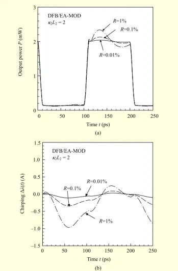
Fig. 7. (a) Output power and (b) chirp of DFB-LD/EA-MOD for various values of output Rf.
Time t (ps) 0 50 100 150 200 250 Outpu t power P (mW) 0 1 2 3 DFB/EA-MOD κ2L2 = 2 R=1% R=0.01% R=0.1% (a) Time t (ps) 0 50 100 150 200 250 –1.5 –1.0 –0.5 0.0 0.5 1.0 1.5 DFB/EA-MOD κ2L2 = 2 R=1% R=0.01% R=0.1% Chirping Δ λ( t) (A) (b)
decreased linearly during an on-state and decreased exponentially during an off-state.
Figure 6 shows the static ER and slope efficiency during an on-state of the DFB-LD/EA-MOD and DR-LD/EA-MOD for various values of κ2L2. As κ2L2 increases, for the
DR-LD/EA-MOD, the ER is nearly constant and the slope efficiency is decreased linearly, but, for the DFB-LD/EA-MOD, the ER is changed irregularly and the slope efficiency is decreased nonlinearly with the maximum value occurring at a κ2L2 of
1.25. This irregular change in the ER for the DFB-LD/EA-MOD is mainly due to the variation in the output power during an on-state, which results from the optical reflection from the output facet. In this simulation, the ER is calculated from the output power difference between the on-state and off-state at the front facet of the EA-MOD. Unlike the value calculated from Fig. 3, that is, approximately 10 dB, an ER of 11.6 dB to 11.9 dB is obtained for both devices. This effect (that is, the change in the ER owing to the residual facet reflection) can be explained by the variation in the photon distribution during
Fig. 8. (a) Output power and (b) chirp of DR-LD/EA-MOD for various values of output Rf.
Time t (ps) 0 50 100 150 200 250 Pow er P (mW) 0 1 2 3 DR/EA-MOD κ1L1 = 6 κ2L2 = 2 R=1% R=0.01% R=0.1% (a) Time t (ps) 0 50 100 150 200 250 –1.5 –1.0 –0.5 0.0 0.5 1.0 1.5 R=1% R=0.01% R=0.1% DR/EA-MOD κ1L1 = 6 κ2L2 = 2 Chirping Δ λ( t) (A) (a)
the on-state and off-state, that is, linear and exponential decreases.
Figures 7 and 8 show the transient output power and wavelength chirp of the DFB-LD/EA-MOD and the DR-LD/EA-MOD at a rate of 10 Gb/s for various values of the output Rf, respectively. The current injected into the active
region is controlled such that an output power of 2 mW can be achieved. The simulation results show that the power fluctuation and chirp of the DR-LD/EA-MOD are reduced more than those of the DFB-LD/EA-MOD under the same reflectivity. This means that the carrier densities within the active region of DR-LD are less fluctuated for the optical signal reflected back into the active region. In this simulation, it is found that the phase of the optical signal reflected from the output facet has an additional influence on the output power fluctuation and chirp. The detailed explanations and results for this appear in [18].
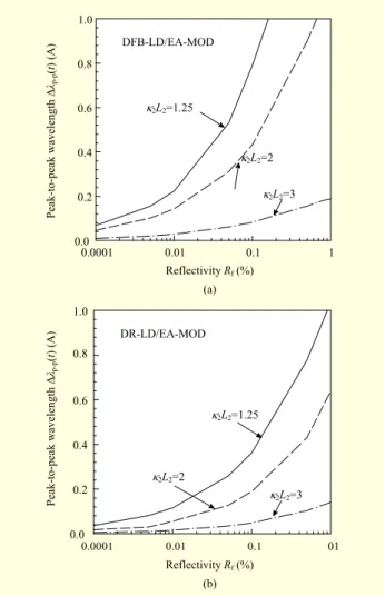
Figure 9 shows the peak-to-peak wavelengths of the DFB-LD/EA-MOD and the DR-DFB-LD/EA-MOD as a function of the
Fig. 9. Peak-to-peak wavelengths of (a) DFB-LD/EA-MOD and (b) DR-LD/EA-MOD as function of output Rffor various
values of coupling coefficient of active region (κ2L2 = 1.25, 2, 3). Reflectivity Rf (%) 0.0001 0.01 0.1 1 Peak-to-peak wavelength Δ λp-p (t ) (A) 0.0 0.2 0.4 0.6 0.8 1.0 DFB-LD/EA-MOD κ2L2=1.25 κ2L2=2 κ2L2=3 (a) 0.0001 0.01 0.1 01 0.0 0.2 0.4 0.6 1.0 DR-LD/EA-MOD 0.8 κ2L2=1.25 κ2L2=2 κ2L2=3 Reflectivity Rf (%) (b) Peak-to-peak wavelength Δ λp-p (t ) (A)
output Rf for various coupling coefficients (that is, κ2L2 = 1.25,
2, 3). It is shown that the peak-to-peak wavelength of the DR-LD/EA-MOD is half that of the DFB-DR-LD/EA-MOD. To investigate the chirp properties of single-mode integrated laser diodes utilizing the Bragg grating, we divide the chirp obtained through a dynamic analysis, that is, Δλ(t), into the component related to the wavelength dependence of the detuning, that is, deviation from the Bragg condition, Δλδ(t), and the component related to the variation of carrier densities along the active region, ΔλN(t) [19]. Each component can be written as follows.
[
]
[
]
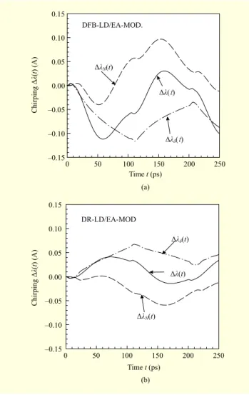
LD LD LD LD ( ) ( ) ( ) 1 ( , ) (0, ) ( ) B ( ) ( , ) (0, ) , ( ) N t t t t z z A BN t t N t z N z A BN t δ λ λ λ δ δ λ Δ = Δ + Δ − = − + − − + (19) whereFig. 10. Chirp and its components of (a) DFB-LD/EA-MOD and (b) DR-LD/EA-MOD. In this simulation, κ2L2 = 2 and
Rf = 0.01%. Time t (ps) 0 50 100 150 200 250 –0.15 –0.10 –0.05 0.00 0.05 0.10 0.15 DFB-LD/EA-MOD. (a) Chirping Δ λ( t) (A) ΔλN(t) Δλ(t) Δλδ(t) Time t (ps) 0 50 100 150 200 250 –0.15 –0.10 –0.05 0.00 0.05 0.10 0.15 DR-LD/EA-MOD Chirping Δ λ( t) (A) Δλδ(t) Δλ(t) ΔλN(t) (b) 2 02 2 , , 2 ( ) g H n dg A B dN t π α λ λ Γ = =
where the first term of (19) indicates the temporal variations of the detuning, namely, changes in the difference between the lasing wavelength and Bragg wavelength, and the second term represents the temporal variations in the (threshold) carrier densities from the residual facet reflection. In addition, zLD
represents the position between the LD and the EA-MOD. Figure 10 shows the chirp and its components of the DFB- LD/EA-MOD and the DR-LD/EA-MOD at a reflectivity Rf of
0.01%. In this condition, the effect of Δλδ(t) is comparable to that of ΔλN (t). During a transient condition near 100 ps, that is,
from an off-state to an on-state, for the DFB-LD/EA-MOD, ΔλN (t) is shifted to a longer wavelength owing to the decrease
of the carrier densities by the increase of the facet reflection, and Δλδ(t) is shifted to a shorter wavelength owing to the increase of the detuning. For the DR-LD/EA-MOD, the chirp and its components show opposite properties of those of
DFB-LD/EA-MOD. This result can be explained by the difference in the propagation constants between the active region (β2) and
passive reflector (β1) [20]. Therefore, the transient wavelength
of the DR-LD/EA-MOD appears to be longer at the leading edge of the pulse and shorter at the falling edge. From this result, it can be thought that the optical pulse provided by the DR-LD/EA-MOD can provide an enhanced transmission distance from the compensation of the dispersion of the fiber.
IV. Conclusion
We proposed a DR-LD/EA-MOD to improve output efficiency, single-mode yield, and chirp. The proposed device can be useful for practical applications since it can be easily fabricated by the selective MOVPE technique, that is, the control of the width of the SiO2 mask, and its fabrication
process is almost the same as that in the conventional DFB-LD integrated EA-MOD except for the asymmetric coupling coefficient grating structure. For our study, an accurate time-domain transfer-matrix-based laser model was developed. Based on this model, we performed steady-state and large-signal analyses. The performances of the proposed laser, such as the output power, ER, and chirp, were compared with those of an EML. Under a 10-Gbps NRZ modulation, we found that the proposed laser can be 30% higher in output power and about 50% lower in chirp than a conventional EML. In particular, the simulation results show that the chirp provided by the proposed laser appears to have a longer wavelength at the leading edge of the pulse and a shorter wavelength at the falling edge. Therefore, we conclude that both the power consumption and transmission distance can be considerably enhanced by utilizing this laser.
References
[1] D. Marcuse, “DFB Laser with Attached External Intensity Modulator,” IEEE J. Quantum Electron., vol. 26, no. 2, Feb. 1990, pp. 262-269.
[2] M. Aoki et al., “InGaAs/InGaAsP MQW Electroabsorption Modulator Integrated with a DFB Laser Fabricated by Band-Gap Energy Control Selective Area MOCVD,” IEEE J. Quantum
Electron., vol. 29, no. 6, June 1993, pp. 2088-2096.
[3] O. Sahlen, “Optimization of DFB Lasers Integrated with Frantz-Keldysh Absorption Modulators,” J. Lightw. Technol., vol. 12, no. 6, June 1994, pp. 969-976.
[4] M. Yamaguchi et al., “Requirements for Modulator-Integrated DFB LD’s for Penalty-Free 2.5-Gb/s Transmission,” J. Lightw.
Technol., vol. 13, no. 10, Oct. 1995, pp. 1948-1954.
[5] Y.H. Kwon et al., “40 Gb/s Traveling-Wave Electroabsorption Modulator-Integrated DFB Lasers Fabricated Using Selective
Area Growth,” ETRI J., vol. 31, no. 6, Dec. 2009, pp. 765-769. [6] C. Sun et al., “Influence of Residual Facet Reflection on the
Eye-Diagram Performance of High-Speed Electroabsorption Modulated Lasers,” J. Lightw. Technol., vol. 27, no. 15, Aug. 2008, pp. 2970-2976.
[7] M. Aoki et al., “New Transmission Simulation of EA-Modulator Integrated DFB-Lasers Considering the Facet Reflection-Induced Chirp,” IEEE Photon. Technol. Lett., vol. 9, no. 3, Mar. 1997, pp. 380-382.
[8] B.H. Park et al., “Investigation of Optical Feedback in High Speed Electroabsorption Modulated Lasers with a Window Region,”
IEEE Photon. Technol. Lett., vol. 17, no. 4, Apr. 2005, pp.
777-779.
[9] R.A. Salvatore and R.T. Sahara, “Reduction in Reflection-Induced Chirp from Photonic Integrated Sources,” IEEE Photon. Technol.
Lett., vol. 14, no. 12, Dec. 2002, pp. 1662-1664.
[10] H. Soda et al., “Stability in Single Longitudinal Mode Operation in GaInAsP/InP Phase-Adjusted DFB Lasers,” IEEE J. Quantum
Electron., vol. 23, no. 6, June 1987, pp. 804-814.
[11] O.K. Kwon et al., “Effects of Asymmetric Grating Structures on Output Efficiency and Single Longitudinal Mode Operation in
λ/4-Shifted DFB Laser,” IEEE J. Quantum Electron., vol. 47, no. 9, Sept. 2011, pp. 1185-1194.
[12] N. Kim et al., “Widely Tunable 1.55-μm Detuned Dual-Mode Laser Diode for Compact Continuous-Wave THz Emitter,” ETRI
J., vol. 33, no. 5, Oct. 2011, pp. 810-813.
[13] K. Komori et al., “Single-Mode Properties of Distributed-Reflector Lasers,” IEEE J. Quantum Electron., vol. 25, no. 6, June 1989, pp. 1235-1244.
[14] J.I. Shim et al., “Lasing Characteristics of 1.5 μm GaInAsP-InP SCH-BIG-DR Lasers,” IEEE J. Quantum Electron., vol. 27, no. 6, June 1991, pp. 1736-1745.
[15] G.L. Li et al., “Ultra-Speed Traveling-Wave Electroabsorption Modulator-Design and Analysis,” IEEE Trans. Microw. Theory
Techn., vol. 47, no. 7, July 1999, pp. 1177-1183.
[16] O.K. Kwon et al., “Improvement of Modulation Bandwidth in Electroabsorption-Modulated Laser by Utilizing the Resonance Property in Bonding Wire,” Opt. Express, vol. 20, no. 11, May 2012, pp. 11806-11812.
[17] P.J. Steven et al., “Computer Modeling of the Electric Field Dependent Absorption Spectrum of Multiple Quantum Well Material,” IEEE J. Quantum Electron., vol. 24, no. 10, Oct. 1988, pp. 2007-2016.
[18] O.K. Kwon, Y.S. Beak, and Y.C. Chung, “Electroabsorption Modulated Laser with High Immunity to Residual Facet Reflection,” IEEE J. Quantum Electron., vol. 48, no. 9, Sept. 2012, pp. 1203-1213.
[19] J. Kinoshita, “Modeling of High-Speed DFB Lasers Considering the Spatial Holeburning Effect Using Three Rate Equations,”
IEEE J. Quantum Electron., vol. 30, no. 4, Apr. 1994, pp.
929-938.
[20] K. Kudo, S. Arai, and J.I. Shim, “Linewidth Reduction of DSM Lasers Due to Effects of Composite Cavity and Distributed Reflectors,” IEEE J. Quantum Electron., vol. 29, no. 6, June 1993, pp. 1769-1781.
Oh Kee Kwon received his BS and MS in electronics engineering from Hanyang University, Rep. of Korea, in 1996 and 1998 and his PhD in electrical engineering from the Korea Advanced Institute of Science and Technology (KAIST), Daejeon, Rep. of Korea, in 2012. In 2002, he joined the Basic Communication Research Lab. of ETRI, Daejeon, Rep. of Korea, where he has been engaged in research and development of wavelength tunable lasers, wavelength selective switches, and high-speed EML arrays. His current research interests include the characterization of monolithically integrated devices using lasers and amplifiers.
Yong Soon Baek received his BS in physics from Seoul National University, Seoul, Rep. of Korea, in 1991 and his PhD for research in nonlinear optics from CREOL at the University of Central Florida, Orlando, FL, USA, in 1997. In 1999, he joined the Basic Communication Research Lab., ETRI, Daejeon, Rep. of Korea. He has been engaged in the development SOA-related functional devices, optical transceivers for FTTH applications, and advanced optical switches for ROADM systems. He is currently involved in the development of 100-Gbps Ethernet transceiver modules.
Yun C. Chung is a professor of electrical engineering at the Korea Advanced Institute of Science and Technology (KAIST), which he joined in 1994. From 1987 to 1994, he was with the Lightwave Systems Research Department at AT&T Bell Laboratories. From 1985 to 1987, he was with the Los Alamos National Laboratory under the AWU-DOE Graduate Fellowship Program. His current research activities include high-capacity WDM transmission systems, all-optical WDM networks, optical performance monitoring techniques, WDM passive optical networks, and fiber-optic networks for wireless communications. He has published over 400 journal and conference papers in these areas and holds over 60 patents. Prof. Chung is a fellow of IEEE and OSA and a member of the Korean Academy of Science and Technology.
Hyung-Moo Park received his BSc in electrical engineering from Seoul National University, Seoul, Rep. of Korea, in 1978, and his MSc and PhD in electrical engineering from the Korea Advanced Institute of Science & Technology (KAIST), Seoul, Rep. of Korea, in 1980 and 1984, respectively. He has been with the School of Electrical Engineering and Computer Science, Dongguk University, Seoul, Rep. of Korea since 1998. From 1984 to 1998, he was with ETRI, Daejeon, Rep. of Korea, where he served as a senior vice president and was responsible for running the division of materials and components. He is an IEE fellow. He has been engaged in research on compound semiconductor devices for microwave circuits and optoelectronics for optical fiber communications. He has published papers and patented inventions in several fields, including HBT (heterojunction bipolar transistor), MMIC (microwave monolithic integrated circuit), long wavelength InP semiconductor laser diode, and OEIC (optoelectronic integrated circuit). His current research interests include III-V semiconductor technology, microwave and millimeter wave devices, and high power semiconductor devices.