First-principles calculation of capacitance including interfacial effects
Bora Lee, Choong-Ki Lee, Seungwu Han, , Jaichan Lee, and Cheol Seong Hwang
Citation: Journal of Applied Physics 103, 024106 (2008); doi: 10.1063/1.2832413 View online: http://dx.doi.org/10.1063/1.2832413
View Table of Contents: http://aip.scitation.org/toc/jap/103/2 Published by the American Institute of Physics
First-principles calculation of capacitance including interfacial effects
Bora Lee,1Choong-Ki Lee,1Seungwu Han,1,a兲Jaichan Lee,2and Cheol Seong Hwang31
Department of Physics, Ewha Womans University, Seoul 120-750, Republic of Korea
2
School of Materials Science & Engineering, SungKyunKwan University, Suwon 440-746, Republic of Korea
3
School of Materials Science and Engineering, and Inter-University Semiconductor Research Center, Seoul National University, Seoul 151-742, Republic of Korea
共Received 6 September 2007; accepted 14 November 2007; published online 31 January 2008兲 An efficient computational method is proposed within a first-principles framework to calculate capacitances of metal-insulator-metal structures including interfacial effects. In this approach, we employ metal-insulator models under external electric fields to calculate dielectric responses near the interface region. Macroscopically averaged potentials allow for evaluating the capacitance and local dielectric constants of the corresponding metal-insulator-metal capacitor. We apply this method to calculate the capacitance of Au/MgO共100兲/Au and Ni/ZrO2共110兲/Ni with dielectric thicknesses of nanometers. While the Au/MgO interface is relatively free of interfacial effects, the computational results for Ni/ZrO2 indicate the presence of interfacial regions with dielectric constants noticeably lower than that of the bulk. Microscopic origins are discussed. © 2008
American Institute of Physics.关DOI:10.1063/1.2832413兴
I. INTRODUCTION
The dielectric constant is a fundamental quantity that characterizes electrical and optical responses of insulators. Experimentally, it can be measured with a high precision when materials are in bulk phases. However, for microelec-tronic devices or thin-film structures, where insulators are vastly employed, dielectric constants are often scattered de-pending on growth conditions and measurement techniques. Furthermore, it is observed that dielectric constants in metal-insulator-metal共MIM兲 capacitors are affected by the dielec-tric thickness1or the species of electrodes.2This implies that the interface between insulators and metals substantially modify overall dielectric behaviors, which can be understood by high ratios of interface to volume for thin films. However, the understanding of the interfacial effects on dielectric con-stants is often hampered by difficulties in characterizing in-terfacial structures, and it is ambiguous whether the varia-tions in dielectric constants are intrinsic or, for instance, due to the existence of a secondary phase near the interface. As individual components are aggressively scaled down for ad-vanced electronic devices, understanding of the interface property is not only a fundamentally intriguing issue but also crucial for the development of reliable electronic devices.
On the theoretical side, a direct study on dielectric prop-erties of capacitors is complicated by the inherent nonequi-librium condition; the applied bias splits chemical potentials of constituent electrodes. However, this is not compatible with the conventional density functional methods to calculate the ground-state properties since they require a unique Fermi level throughout the whole system.3 Methods based on the nonequilibrium Green’s functions can describe the finite bias, but they are still computationally demanding. Recently, Stengel et al. noticed that the localized character of Wannier
functions can be used to calculate dielectric constants of MIM structures.4 By applying this method to the interfaces between SrTiO3 and various electrodes, they were able to reveal the presence of dielectric dead layers intrinsic to the metal-oxide interfaces.5
In this article, we propose an alternative computational framework based on the first-principles method to calculate dielectric properties or capacitances in consideration of the metal-insulator interface. The simulation of the nonequilib-rium condition is enabled by adopting a metal-insulator共MI兲 slab with both ends exposed to the vacuum, rather than pe-riodically repeated MIM structures. The external bias or po-tential differences between electrodes are emulated by the application of an electric field. Our method exploits features that are already implemented in widely used first-principles codes such as the VIENNA AB INITIO SIMULATION PACKAGE
共VASP兲,6or QUANTUM-ESPRESSO7and therefore could be
em-ployed easily. This paper is organized as follows. In Sec. II, we will outline basic ideas of our theoretical approaches, followed by a detailed computational setup. Exemplary ap-plications to model interfaces of Au/MgO and Ni/ZrO2 are presented in Sec. III with related discussions. Section IV summarizes the main achievements.
II. COMPUTATIONAL METHODS A. Basic models
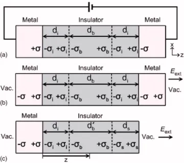
Our method is based on the similarities between a MIM capacitor and its derived metal-insulator共MI兲 slab, as illus-trated in Fig.1. The starting model in Fig.1共a兲schematically represents a typical capacitor connected to an external volt-age source. The interfacial regions with an electrical polariz-ability distinct from the bulk are explicitly described. The applied bias builds up free charges at the metal-insulator in-terface, which in turn induces dielectric polarizations inside the insulator. Discontinuities in the polarization also result in
a兲Author to whom correspondence should be addressed. Electronic mail: [email protected].
effective surface charges at various interfaces present in the model system. The capacitance of this model is then calcu-lated in SI units as follows:
CMIM=
0A
2共−i兲di+共−b兲db
, 共1兲
where0is the vacuum permittivity,and d are the surface charge density and thickness of each region, respectively, and A is the cross-sectional area of the electrode. The sub-scripts i and b in Eq. 共1兲 indicate the interfacial and bulk regions.
The role of the external power source in Fig.1共a兲can be replaced by the external field共Eext兲 applied on the MIM slab model with both ends exposed to the vacuum关see Fig.1共b兲兴. The nonequilibrium condition is maintained as long as the charge transfer between metal electrodes is forbidden.3 How-ever, as mentioned in the Introduction, this is difficult to achieve within the conventional first-principles calculations.
Eext is chosen such that the surface charge density 共兲 in-duced on the metal surface is identical to that in Fig.1共a兲. Then, the other parameters 共i, b, di, and db兲 would not change either. If repeated along the surface normal without the vacuum space, the resulting periodic MIM structure is similar to that used in Refs.4and5.
By removing the right electrode in the isolated MIM model, one arrives at a MI slab model shown in Fig. 1共c兲, which constitutes the base model used in this work. With the same choice of materials and interface types as in the origi-nal MIM capacitor model, the interface properties repre-sented by iand diare equal to those in Fig. 1共a兲. We then define a virtual capacitance C˜MIof the MI model as follows:
C ˜ MI共z兲 = A 2V共z兲= 0A 2共−i兲di+ 2共−b兲共z − di兲 , 共2兲
where V共z兲 is the potential at z from the interface 关see Fig.
1共c兲兴 and evaluated with respect to the potential value inside the metal electrodes. We note that the surface region in Fig.
1共c兲共represented by the index s兲 does not contribute to C˜MI as far as surface effects are negligible at z. By equating Eq.
共2兲 with Eq. 共1兲, a condition, 2z = 2di+ db= d, is obtained where d is the total thickness of the insulator in the MIM model. That is to say, by evaluating V共z兲 and , one can calculate the capacitance of the corresponding MIM structure with an insulator thickness of 2z. Furthermore, is readily obtained from the condition that the electric field vanishes inside the electrodes, which gives =0Eext. Although the model systems in Fig.1 assume discrete interfacial regions, it is straightforward to extend the above formulation to the case of continuously varying polarizations.
B. First-principles implementations
The schematic framework in the previous section can be implemented within the density functional methods. An ato-mistic model is first built up representing the metal-insulator interface with both ends exposed to the vacuum, and a con-stant electric field is applied. To be consistent with the MI model in Fig.1共c兲, it should be confirmed that three kinds of electron transfers do not occur under external fields:共i兲 The electron transfer from the metal to conduction bands of the insulator 共Schottky emission兲. 共ii兲 The transition from va-lence bands to conduction bands of insulators共Zener break-down兲. 共iii兲 The emission of electrons from the metal or in-sulator to the vacuum共field emission兲. These conditions can be verified directly by inspecting the distribution of charge densities and partial density of states.
To obtain V共z兲 in Eq. 共2兲from first-principles results, it is required to make the atomically varying potentials smooth. The local potential is first averaged over the plane perpen-dicular to the surface normal. To extract information relevant to dielectric responses, we calculate the change in electro-static potentials upon the application of electric fields,
⌬V共z兲 = 1 LxLy
冕
0 Lx dx冕
0 Lydy关Vloc共x,y,z;Eext兲
− Vloc共x,y,z;0兲兴, 共3兲
where Lxand Lyare the unit cell lengths along the x and y directions, and Vloc共x,y,z;E兲 is the sum of ionic and Hartree potentials under an external field of E. The ions could be fixed to their equilibrium positions at zero bias or relaxed in response to the finite electric fields. Each corresponds to the dielectric response at optical frequencies 共⬁兲 or for static fields 共0兲, respectively. When ionic relaxations are consid-ered to calculate 0, ⌬V共z兲 is oscillatory due to small dis-placements of ions. This can be smoothened through a mac-roscopic average8 along the z-direction,
FIG. 1. 共Color online兲 Schematic pictures explaining the computational framework. 共a兲 A conventional MIM capacitor connected to an external voltage source.共b兲 The electric bias is replaced by an external field which produces the same surface charge density as in 共a兲. 共c兲 The metallic electrode on the right-hand side is removed from the MIM model in共b兲. All constituent materials and interface types are assumed to be identical among model systems.
具⌬V共z兲典 = 1 l1l2
冕
z−共l1/2兲 z+共l1/2兲 dz⬘
冕
z⬘−共l2/2兲 z⬘+共l2/2兲 dz⬙
⌬V共z⬙
兲, 共4兲where l1 and l2 are the periodicity lengths along the
z-direction for the metal and insulator in bulk phases,
respec-tively. As will be shown below, 具⌬V共z兲典 changes smoothly inside the electrodes and insulators, thereby allowing for as-signing potential values关V共z兲兴 inside the insulator to be used in Eq. 共2兲. In addition, one can define local dielectric con-stants as follows:
具共z兲典 = Eext/
d
dz具− ⌬V共z兲典. 共5兲
The concept of local dielectric constants was first introduced for periodic insulating systems in Refs. 9 and10. In those works, the permittivity profiles were evaluated from local polarizations which were in turn obtained by induced charge densities. In the present formulation, the differential electro-static potential in Eq.共3兲is contributed by the same induced charges. Therefore, the local dielectric constant defined in Eq. 共5兲 is equivalent to that formulated in Ref.9. The only difference that can be expected is from technical details such as how the potentials or charge densities are averaged. In passing, we add that the above computational approach can be used to evaluate dielectric constants of bulk insulators as long as the slab is thick enough.
One of the advantages in our method is that it can be easily adopted using conventional codes without any major modification. However, some technical considerations are re-quired for free surfaces of insulators present in the model system. 共This was also noted in Ref. 4.兲 If the
bulk-terminated surface of the insulator is polar, a surface passi-vation is required to satisfy electron counting rules and make the surface insulating. This can be achieved in various ways. As an example, attaching hydrogen atoms makes MgO共111兲 surface insulating.11Alternatively, one can control the sto-ichiometry to neutralize the surface. For instance, the cubic-ZrO2共100兲 surface becomes insulating if one oxygen atom is removed from the O-terminated surface unit cell. As another example, the AlO2 face of the LaAlO3共100兲 surface can be neutralized by removing one oxygen atom from the 共2⫻2兲 surface unit cell. For ferroelectric materials, however, the bulk property may not be recovered inside the slab.12 There-fore, extra caution is demanded when calculating on ferroelectric-metal interfaces.
C. Model systems
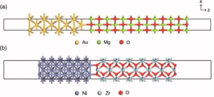
For specific models to apply our methods, we choose Au/MgO共100兲 and Ni/cubic-ZrO2共110兲 interfaces 共see Fig.
2兲. The numbers of atoms within the unit supercell are 34
and 65 for Au/MgO and Ni/ZrO2, respectively. The lattice mismatch between the metal and oxide is within 1% and the in-plane lattice parameters are set to those of oxides. For density functional calculations, we employVASP throughout this work. The ionic potentials are described by the projector-augmented-wave method,13 and the exchange-correlation energies of electrons are described within the lo-cal density approximation.14The energy cutoff of 400 eV is
used to generate a plane-wave basis set to expand the wave functions. For the k-point integration, 6⫻6⫻1 and 4⫻6 ⫻1 regular meshes are used for Au/MgO and Ni/ZrO2, re-spectively. The density of states is broadened by the Gauss-ian function with a width of 0.05 eV. The vacuum lengths between neighboring supercells are longer than 14 Å to avoid the wave function overlap. The external bias is simu-lated with a sawtooth potential to be compatible with peri-odic boundary conditions. The external field induces dipole moments within the model slab, giving rise to spurious long-range dipole-dipole interactions between model slabs. In or-der to prevent the cross talk between supercells, artificial dipoles are introduced in the middle of the vacuum region to cancel out dipole fields from other slabs.15The atomic coor-dinates are relaxed until the Hellmann-Feynman forces for each atom are reduced to within 0.02 eV/Å.
III. RESULTS AND DISCUSSIONS A. Au/MgO„100… interface
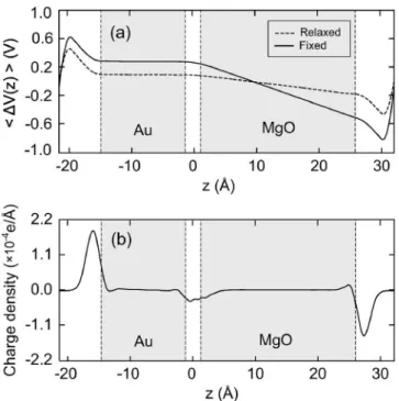
We first discuss on computational results for the Au/ MgO共100兲 interface. The equilibrium geometry indicates that the distance between the outermost metal layer and the Mg共O兲 atom in the adjacent layer is 2.46 共2.51兲 Å. Figure
3共a兲 shows 具⌬V共z兲典 when an external field of 0.1 V/Å is applied along the normal direction of the interface 共z-direction兲. The solid line indicates results obtained with fixed ionic positions while the dashed line is calculated with all atoms fully relaxed. The smooth change of 具⌬V共z兲典 throughout the model system permits an unambiguous deter-mination of capacitances following the formulation given in the previous section. The almost flat potential in the metallic region is indicative of the perfect metallic screening. Inside the insulator, on the other hand, the external field is screened by induced dipole moments, and the internal fields are about 0.03 and 0.01 V/Å for fixed and relaxed results. In Fig.
3共b兲, field-induced redistributions of charge densities are dis-played. The accumulation of electronic charges at the surface of the metal electrode is calculated to be 4.71⫻10−3 e/Å2in comparison with 4.83⫻10−3 e/Å2 estimated directly from the external electric field共see above兲.
In Fig. 4共a兲, the inverse of local dielectric constants 共具共z兲典−1兲 is shown. On the metallic side, 具共z兲典−1is close to zero, consistent with the perfect metallic screening. Inside the dielectric, on the other hand, 具共z兲典−1 rapidly converges to a finite value. The optical and static dielectric constants
FIG. 2. 共Color online兲 The model interfaces calculated in this work. 共a兲 Au/MgO共100兲; 共b兲 Ni/ZrO2共110兲.
evaluated in the middle of the MgO slab are 3.36 and 9.65, respectively. These values as well as the profile of具共z兲典−1in Fig.3共a兲are in good agreement with the results for the cor-responding Ag/MgO/Ag capacitor in Ref.4 calculated with Wannier functions, suggesting that interface properties are well captured in our methods.
The inverse capacitance per unit area and the nominal dielectric constant, which is equal to dC/A, are calculated with respect to the dielectric thickness of the corresponding Au/MgO/Au capacitor. Figure4共b兲shows the results at high frequencies obtained from具⌬V共z兲典 with fixed ionic positions,
while the fully relaxed results are employed to obtain the plots in Fig.4共c兲. To define the insulator thickness, the origin corresponding to z = 0 is set to the middle of the interface layers共see Fig.3兲. We recall that the thickness 共d兲 is equal to
2z if V共z兲 is used in evaluating the capacitance based on Eq.
共2兲.
For the sake of analysis, we schematically represent the capacitance including interface regions as follows:
1 C= 1 Ci + 1 Cb + 1 Ci = 1 A0
冋
2di冉
1 i − 1 b冊
+ d b册
, 共6兲where di is the interface thickness, and i共b兲 indicates the dielectric constants for the interfacial共bulk兲 regions, respec-tively. Equation 共6兲 means that the A/C-vs-d graph crosses the origin if the interfacial effects are negligible 共di= 0 or i=b兲. In fact, it can be observed in Figs.4共b兲and4共c兲that the extrapolated inverse capacitances narrowly pass through the origin, indicating that the thickness of the interfacial re-gions is small for both optical and static frequencies. Con-sistently, the nominal dielectric constants are almost constant with respect to d, as shown in the same figures. The effective dielectric constantsbobtained from linear fits of共C/A兲−1vs
d are 3.22 and 9.56 for optical and static results, respectively,
in good agreement with 3.36 and 9.65 obtained directly from 具共z兲典.
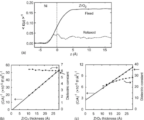
B. Ni/ ZrO2 interface
For another application, we calculate on Ni/cubic-ZrO2共110兲 as shown in Fig. 2共b兲. ZrO2 is a candidate re-placement oxide to be used in future microelectronic devices.16 The relaxed structure shows that the Zr and O atoms in the interface layer are at distances of 1.95 and 1.87 Å from the boundary of the electrodes, respectively. The buckling tendency is opposite to that of the Au/MgO interface where the cation is closer to the metal共see above兲, and this reflects that the surface reactivity is higher for
FIG. 3. 共a兲 具⌬V共z兲典 for the Au/MgO共100兲 model slab. The external field is 0.1 V/Å. The vertical dashed lines indicate the position of boundary layers of the insulator and the metal.共b兲 The induced charge density is shown. The ions are fixed to their equilibrium positions.
FIG. 4.共a兲 The inverse of local dielec-tric constants for the Au/MgO共100兲 in-terface with ions fixed共solid line兲 or relaxed共dashed line兲. 共b兲 The inverse capacitances and nominal dielectric constants at optical frequencies are shown with respect to the thickness of MgO in the corresponding symmetric Au/MgO/Au capacitor. The bulk di-electric constant is indicated by an ar-row on the right axis. 共c兲 Similar graphs at the static frequency.
ZrO2共110兲 than MgO共100兲. In addition, it is found that the local structures are slightly distorted from the cubic phase to the tetragonal phase. This is due to the unstable phonon mode in cubic ZrO2triggering a transition into the tetragonal phase. However, the relative oxygen displacement is only 0.0005 in comparison with the theoretical value of 0.04 in the crystalline tetragonal phase.17 Therefore, material prop-erties are expected to be very close to those of the cubic phase. In Fig. 5共a兲, we plot the inverse of the computed 具共z兲典. The dielectric constants measured in the middle of ZrO2 are 6.23 and 36.1 for ⬁ and 0, respectively. These values are in good agreement with 5.75 and 35.52 calculated using the Born effective charges and phonon modes at the zone center.17 On the other hand, it is noticeable that the dielectric constants are substantially reduced near the inter-face region. This is contrasted to the fixed results, which show a monotonic transition from the metal to dielectric and therefore do not show interfacial effects in the inverse ca-pacitance curve in Fig.5共b兲. Due to the presence of the low-permittivity regions at the interface, the dielectric constants in Fig. 5共c兲 are substantially smaller than the bulk value when ZrO2 is thinner than 2 nm. Consistently, the inverse capacitance is extrapolated to a finite value at the zero thick-ness, which suggests the presence of an interfacial layer based on Eq.共6兲. The dielectric constant calculated from the slope of the inverse capacitance is 37.1, close to the value of 36.1 above.关The slope of the inverse capacitance in Fig.5共b兲 results in⬁of 5.97 in accord with the value of 5.75 above.兴 To gain some insight into the origin of the reduced in-terfacial dielectric constants for Ni/ZrO2, we carry out a fur-ther analysis on the computational results. First, the screen-ing property of electrodes is checked because the incomplete metallic screening can give rise to interfacial capacitances.18 To this end, we note that the interfacial effects are not sig-nificant for the optical dielectric constants 关see Fig. 5共b兲兴, although the具共z兲典−1profile from the interface共z=0兲 into the
metal side is very close to that for the static dielectric con-stants. Therefore, it can be concluded that the reduction of the dielectric constants for Ni/ZrO2originates from the ma-terial properties of ZrO2 at the interface region that are at variance with the bulk.
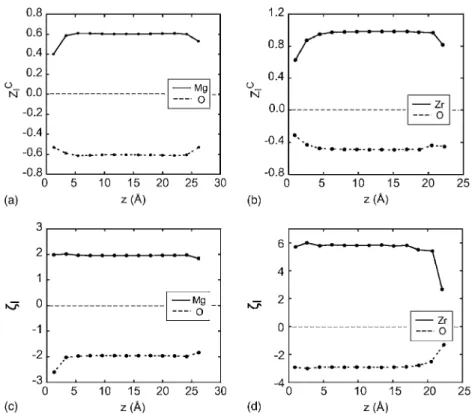
In general, the ionic parts of static dielectric constants are determined by effective charges and frequencies of the phonon modes related to dielectric relaxations. Therefore, any changes in these quantities lead to variations in the di-electric constants. In Ref.5, for example, it was shown that the hardening of the soft phonon modes in SrTiO3 is the main origin of the intrinsic dead layer pertaining to the metal-SrTiO3 interfaces. The investigation of the local pho-non modes at the interface is beyond the scope of the current work. Instead, we examine the spatial variations of effective charges. In Figs.6共a兲and6共b兲, the zz components of Callen dynamical charges 共ZI
C兲 are shown for the atom I in the in-sulator part.9,19In our model systems, ZI
C
is computed by the
z-component of the Hellmann-Feynman force divided by the
external field. As shown in Figs. 6共a兲 and 6共b兲, the Callen charges are significantly smaller at the interface region. However, the Callen charges are affected by local electric fields, and we calculate in Figs.6共c兲and6共d兲another effec-tive charge I=⬁共zI兲ZI
C
that is directly related to effective ionic polarizabilites.9 It is notable thatI is almost constant from the interface to the bulk for both the Au/MgO and Ni/ZrO2 interfaces. 共However, a slight decrease of I is noted for the O atom at the Au/MgO interface.兲 This strongly suggests that the reduction of dielectric constants in Ni/ZrO2 is likely to be caused by hardening of the soft modes in cubic ZrO2. Further analysis on local phonon modes will be able to verify this.
IV. SUMMARY
To summarize, we have proposed a simple but efficient first-principles approach to calculate dielectric constants in
FIG. 5. 共a兲 The inverse of the local dielectric constant for Ni/ZrO2共110兲 interface.共b兲 The inverse capacitances and nominal dielectric constants at op-tical frequencies are shown with re-spect to the thickness of ZrO2in the corresponding symmetric Ni/ZrO2/Ni capacitor. The bulk dielectric constant is indicated by an arrow on the right axis. 共c兲 Similar graphs at the static frequency.
consideration of interfacial effects. Our results were in good comparison with the available results obtained by Wannier functions. In the case of a Au/MgO interface, the interfacial effect was negligible, while the local dielectric constant for a Ni/ZrO2interface shows a signature of intrinsic dead layers. The effective charges are almost constant throughout the model systems except for the surface region. This implies that the hardening of phonon modes should be the most im-portant origin.
ACKNOWLEDGMENTS
This work was supported by the System IC2010 program of the Korean government and by the KOSEF through Na-tional Research Laboratory 共NRL兲 program. The authors would like to acknowledge the support from KISTI Super-computing Center共KSC-2007-S00-1006兲.
1C. S. Hwang, J. Appl. Phys. 92, 432共2002兲.
2O. G. Vendik, S. P. Zubko, and L. T. Ter-Martirosayn, Appl. Phys. Lett.
73, 37共1998兲.
3N. Nakaoka, K. Tada, S. Watanabe, H. Fujita, and K. Watanabe, Phys. Rev. Lett. 86, 540共2001兲.
4M. Stengel and N. A. Spaldin, Phys. Rev. B 75, 205121共2007兲. 5M. Stengel and N. A. Spaldin, Nature共London兲 443, 679 共2006兲. 6G. Kresse and J. Hafner, Phys. Rev. B 47, 558共1993兲; G. Kresse and J.
Hafner, ibid. 49, 14251共1994兲.
7S. Baroni, A. Dal Corso, S. de Gironcoli, and P. Giannozzi, http:// www.pwscf.org
8A. Balderschi, S. Baroni, and R. Resta, Phys. Rev. Lett. 61, 734共1988兲. 9F. Giustino and A. Pasquarello, Phys. Rev. B 71, 144104共2005兲. 10F. Giustino and A. Pasquarello, Phys. Rev. Lett. 95, 187402共2005兲. 11Y. Cho, C. Kim, H.-S. Ahn, E. Cho, T. Kim, and S. Han, J. Appl. Phys.
101, 083710共2007兲.
12B. Meyer and D. Vanderbilt, Phys. Rev. B 63, 205426共2001兲. 13P. E. Blöchl, Phys. Rev. B 50, 17953共1994兲.
14D. M. Ceperley and B. J. Alder, Phys. Rev. Lett. 45, 566共1980兲. 15L. Bengtsson, Phys. Rev. B 59, 12301共1999兲.
16Y. F. Dong, S. J. Wang, J. W. Chai, Y. P. Feng, and A. C. H. Huan, Appl. Phys. Lett. 86, 132103共2005兲.
17G.-M. Rignanese, F. Detraux, X. Gonze, and A. Pasquarello, Phys. Rev. B
64, 134301共2001兲.
18C. T. Black and J. J. Welser, IEEE Trans. Electron Devices 46, 776共1999兲. 19Ph. Ghosez, J.-P. Michenaud, and X. Gonze, Phys. Rev. B 58, 6224
共1998兲.
FIG. 6. 共a兲, 共b兲 The zz component of Callen charge共ZI
C兲 for the atom I at a
distance z from the interface of Au/ MgO and Ni/ZrO2, respectively. 共c兲, 共d兲 Effective charges I obtained by
multiplying ZI
C with optical dielectric
constants at the ionic position for Au/ MgO and Ni/ZrO2, respectively.