P2-84 / H. Lee
IMID 2009 DIGEST •
Abstract
Organic light emitting layer in OLED device was formed by gravure printing process in this work. Organic surface coated by gravure printing typically showed relatively bad uniformity. Thickness and roughness control was characterized by applying various mixed solvents in this work. Poly (N-vinyl carbazole) (PVK) and fact-tris(2-phenylpyridine)iridium(Ir(ppy)3) are host
dopant system materials. PVK was used as a host and Ir(ppy)3 as green-emitting dopant. To luminance efficiency of the plasma treatment on etched ITO glass and then PEDOT:PSS spin coated.
The device layer structure of OLED devices is as follow Glass/ITO/PEDOT:PSS/PVK+Ir(ppy)3-Active layer /LiF /Al. It was printed by gravure printing technology for polymer light emitting diode (PLED). To control the thickness multi-printing technique was applied. As the number of the printing was increased the thickness enhancement was increased. To control the roughness of organic layer film, thermal annealing process was applied. The annealing temperature was varied from room temperature, 40°C, 80°C, to 120°C.
1. Introduction
Recently, several research groups have demonstrated the feasibility of printing processes for OLED fabrication with ink-jet printing, screen printing, and gravure printing processes. [2,3]. We have developed gravure printing process for organic layer of OLED in this work. We characterized the effects of thermal annealing on nanoscale organic layer thickness and roughness in gravure printing of organic lighting materials. We investigated gravure printing process and post thermal annealing process for the organic layer of OLEDs in this work. We characterized the effects of annealing on the surface morphology and roughness of the nanoscale organic layer in the gravure printing of organic lighting materials.
2. Experimental
The first step of the device fabrication is to pattern ITO coated glasses. 3mm wide and 70mm long line was formed on the center of the 70 x 70 mm2 ITO
glass by masking the ITO bottom electrode with insulation tapes. The substrate was immerged in diluted HCl solution for 15 min at the room temperature. After the etching process, the surface was sequentially cleaned with trichloroethylene, acetone, methanol, and DI-water. Each cleaning process was carried out in ultrasonic bath for 15 min at 40 °C. O2 plasma treatment was applied to the
patterned ITO anode to remove the carbon contamination. O2 plasma treatment is also known to
increase the work function and to improve the maximum lifetime. An inductively coupled plasma reactor was used for the plasma treatment process at a pressure of 20mTorr with a source power of 100watts, O2 flow rate of 15 sccm, and Ar flow rate of 15 sccm
for 5min. After the plasma treatment, a PEDOT:PSS (Baytron P) layer formed by the spin-coating process. The active layer was formed by the gravure printing process in this work.
The gravure printer used in this work was custom-made by Samjung MachineryTM. It consisted of a
gravure roll, doctor blade, silicone roll, and substrate. The substrate was inserted between the patterned roll and silicone transfer roll. The pressure between the patterned roll and silicone roll was kept at 6.5 MPa and the blade pressure at 1.5 MPa. The printing speed was used 83 rpm or 217mm/s in linear velocity. The engraved pattern on the printing roll was filled with ink by dropping. The thickness was increased by increasing the number of printings.
To control the roughness and morphology of organic
Effect of Thermal Annealing on Nanoscale Thickness and
Roughness Control of Gravure Printed Organic Light
Emitting for OLED with PVK and Ir(ppy)
3Hyemi Lee, Aran Kim, Dae Kyoung Kim ,Sung Min Cho, and Heeyeop Chae* School of Chemical Engineering, Sungkyunkwan University
Suwon, 440-746, Korea
P2-84 / H. Lee
• IMID 2009 DIGEST
layer film, thermal annealing process was applied. The annealing temperature was varied from room temperature, 40°C, 80°C, to 120°C in hot plate. Active layer was gravure printed and then evaporation in the N2 glove box atmosphere. After the Active layer dry
device was annealing treated between 20min. Young joo lee and coworkers also determined appropriate thermal annealing temperature was reported. They were annealed at the temperatures below and above the glass transition temperatures of each organic layer. TPD glass transition temperature was (Tg=60 °C). [4] After the printing process, the cathode layer was completed by the thermal evaporation process of LiF and Al. The base pressure of the thermal evaporation was of the order of 10-5 torr. The thicknesses of the
LiF and Al layers were about 1 nm and 100nm, respectively.
3. Results and discussion
Thermal annealing is known to make surface uniform due to molecular rearrangement. TPD has the lowest glass transition temperature of 60oC among
active materials of PVK, Ir(ppy)3, TPD, and PBD. To
investigate the effect of thermal annealing temperature we changed annealing temperature from room temperature, 40oC, 80oC and to 120oC. The surface energy variation of gravure printed organic layers on annealing temperature was observed with X-ray diffraction spectroscopy. X-ray diffraction spectroscopy was measured after the thermal annealing as shown in Figure 1.
(a)
(b)
Figure1. X-ray diffraction spectrum of thermally annealed gravure printed layers at different temperatures
As the thermal annealing temperature was increased, the peak intensity of 12.66° was increased up to 80°C and clear shift was observed with 120°C condition. 35.2° peak shows the highest intensity at 120°C. Relatively strong variation was observed at the coordinate axis 2θ of 35° and 35.2°.
The surface roughness and morphology were determined with atomic force microscopy (AFM) as a function of annealing temperature as shown in Figure 2. The degree of the crystallization is expected to increase with temperature. However, around 120°C, the polymer chains are seem to be damaged due to high temperature. Or, up to 80°C the thermal annealing helps in rearranging polymer molecules
4 6 8 10 12 14 16 18 20 22 0 50 100 150 200 250 RT 40 80 120 Inten s it y 2dsin 34.0 34.5 35.0 35.5 36.0 0 100 200 300 400 500 In te n s it y 2dsin RT 40 80 120
P2-84 / H. Lee
IMID 2009 DIGEST •
.
Figure2. Annealing temperature dependence on the surface thickness and roughness–AFM Image
The grain shape morphology was disappeared and thickness and roughness was decreased with increased annealing temperature [5]. However, with the 120oC
annealing condition, the polymer chains seem to be broken and too much energy can damage polymer structures. The thickness and roughness variation with thermal annealing process are summarized in Figure 3.
Figure3. Annealing temperature dependence on the surface thickness and roughness trend
At the room temperature, roughness was 9.97nm. Roughness was decreased up to 80oC annealing
temperature treatment but at the 120oC the roughness
was 2.32nm. At the 120oC the roughness was a little
bit increased. At the 80oC annealing treatment, the
active layers thick was measured by 103nm and roughness was measured 1.08nm.
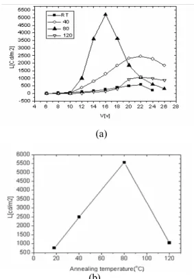
Figure 5 shows luminescence characteristics of various devices annealed at different temperatures.
(a)
(b)
Figure4. OLED brightness dependence on annealing temperature
4. Summary
In this work the effects of solvents and concentration of active materials were studied for gravure printed organic light emitting diodes. In this work we also invested the thermal annealing process after gravure printing of organic layers. We have found that around 80°C is good for PVK and Ir(ppy)3 gravure printed organic layers
Acknowledgement
This work has been carried out with the support of Korea Energy Management Corporation (Project No. 2007-E-CM11-P-07) and also support by the Basic Research Program of the Korea Science & Engineering Foundation (Grand No. R01-2006-000-10140-0).
5. References
1. C. W. Tang and S. A. Van Slyke, Appl. Phys. Lett.,
51(12), 913 (1987)
2. H.Benkreira, R.Patel, Chem.Eng.Sci., 48 2329 (1993)
P2-84 / H. Lee
• IMID 2009 DIGEST
Cho, Curr. Appl. Phsys., 9, 161 (2009)
4. Y.-Joo Lee, H. Lee, Y. Byun , S. Song a, J.E. Kim, D.Eom ,W. Cha, S.S.Park, J. Kim and H.Kim
Thin Solid Films.,515, 5674 (2007)
5. C.Y. Kwong, A.B. Djurisˇic, V.A.L. Roya, P.T. Laia and W.K. Chanc, Thin Solid Films.,458, 281-286(2004)