The effect of smaller output capacitance should be analyzed for stability analysis using an appropriate small-signal resonant LLC converter model. The design of the power stage and feedback loop will be verified by comparing the performance of LLC resonant converters with a switching frequency of 100 kHz and 500 kHz. All design aspects using the GaN E-HEMT are verified with a 240 W prototype LLC resonant converter operating at a switching frequency of 1 MHz.
Introduction
Poor stability due to the small size of the output capacitor is analyzed with the small-signal model. Dominant poles and zeros of the transfer function are measured as the capacitance and ESR value change. In addition, to obtain the output impedance response of the power converter, the step load responses are measured to indirectly verify stable operation.
Design Considerations for High Power Density
Design for Soft Switching Condition
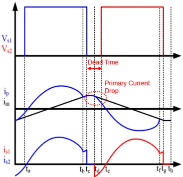
The primary current cannot follow the magnetizing current during the dead time and it is collapsed by the secondary parasitic capacitance before the end of the dead time. The conventional magnetizing inductance design guide shown in (3) has high error to obtain the ZVS condition with high dead time ratio. C (5) Therefore, the magnetizing inductance guaranteeing the ZVS of the MOSFET can be designed considering the high switching frequency operation with long dead time.
Design for Smaller Output Capacitance
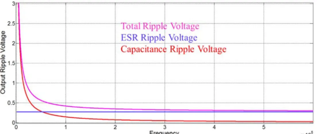
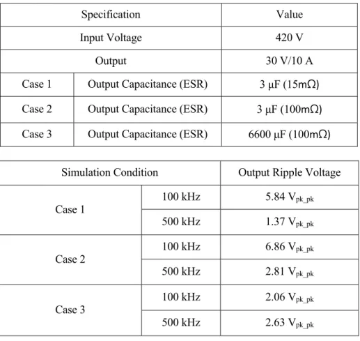
From (6), the voltage ripple related to the output capacitance is proportional to the output current and inversely proportional to the switching frequency. 4 and (6), it is verified that ESR is the dominant factor to reduce the output voltage ripple than the output capacitance at the high switching frequency. Case 2, which has high ESR and low capacitance mode, shows that ESR has a high effect on the output voltage ripple at high switching frequency.
Design for Smaller Transformer
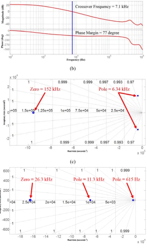
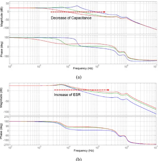
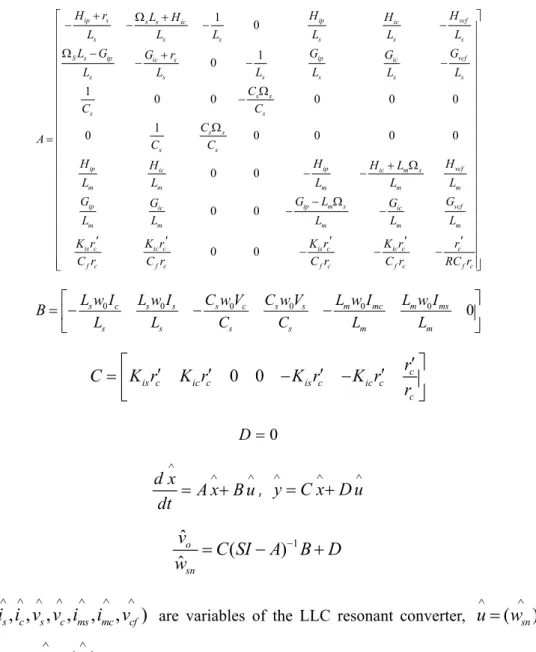
The reduction in transformer size and air gap length is proportional to the square of the switching frequency. The small-signal model of LLC resonant converter has been proposed in previous studies [18]-[21]. 9 shows a comparison of open-loop gain pole placements by output capacitance at 500 kHz switching frequency with pole plot and pole-zero map.
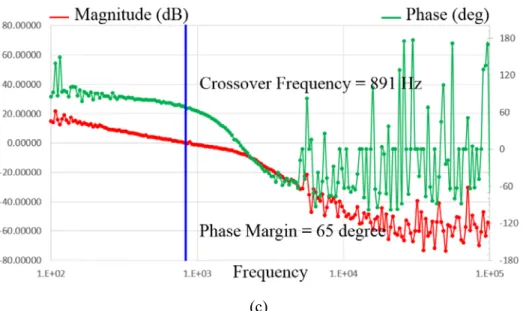
The open loop gain with respect to the output capacitance and the ESR is obtained to analyze the variation of the crossover frequency as shown in Fig. The small output capacitance and small ESR induce a high crossover frequency and drastic decrease of the phase margin. Compared to the 100 kHz switching frequency case, the closed-loop gain of the 500 kHz high frequency LLC resonant converter has much higher crossover frequency to achieve high power density.
Compared to 100 kHz operation, the size of the passive components is drastically reduced when operating at 500 kHz. 21 shows the step load response of the output voltage at a switching frequency of 500 kHz from idle to full load. 34 (a) shows a comparison of transformer and output capacitor sizes with respect to.
To overcome the stability problem, the open-loop gain is investigated to obtain the variation of the crossover frequency and the phase margin according to the output capacitor.
Feedback Control Loop Design
Instability of Power Converter and Derivation of Small-Signal Model
In order to obtain a highly accurate model of the converter, the line resistance and the effective series resistance (ESR) of the output capacitor must be taken into account. In order to achieve a phase margin such as 65° at 100 kHz, the effect of the output capacitance must be considered in order to properly design the feedback compensator for high power density. A small output capacitance results in a much higher frequency location of the first two poles and the zero, resulting in a higher crossover frequency than with a high output capacitance.
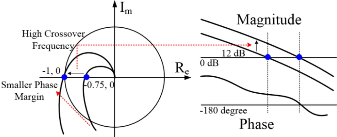
In addition, the effect of the high ESR is investigated to obtain the overall effects of the output capacitor for high power density. The high ESR results in a much lower frequency location of the null, causing a high crossover frequency and high phase margin due to the gradual magnitude slope and earlier phase gain. The small output capacitor causing a high crossover frequency and a low phase margin causes unstable operation of the converter, as shown in Fig.
The nonlinearity induces an undesirable phase drop of the small-signal response, which is significant in the high frequency region. To reduce the side effect of nonlinearity, the crossover frequency should be lower than the Nyquist frequency. Furthermore, to attenuate the high-frequency noise caused by switching devices, the magnitude of the small-signal response of the feedback loop across the crossover frequency must decrease [19].
Finally, the feedback compensator should be designed by considering the above effects to obtain enough phase margin with proper crossover frequency under high power conversion efficiency operation of the LLC resonant converter.
Design of the Feedback Compensator
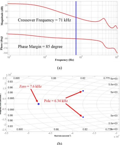
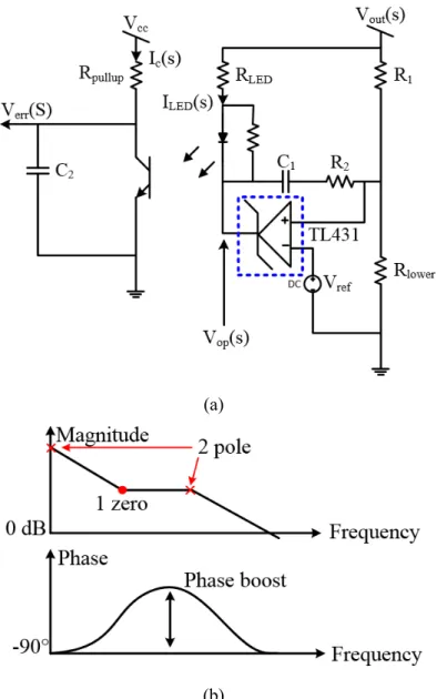
13 Circuit diagram and bode plot of a two-pole zero-feedback compensator: (a) circuit diagram of a two-pole one-zero feedback compensator, (b) bode plot of a two-pole one zero-feedback compensator compensator. The closed-loop crossover frequency (5 kHz) should be chosen to obtain sufficient phase margin through the feedback compensator, which is configured with two poles and one zero. To achieve the lower crossover frequency that is not affected by the nonlinearity effect, the size of the closed loop should be smaller than the size of the open loop gain.
However, the size reduction is limited by the values of RLED and Rpullup of the compensator, as shown in Fig. The high resistance of RLED to reduce the magnitude of the open loop gain prevents current flow to the optocoupler, which requires 0.15 mA as a minimum current. Therefore, 5 kHz is chosen as the lowest crossover frequency, which is slightly below the resonant frequency of the output filter.
Using boost, the coefficient of the K-factor approximation, Kboost, can be determined to specify the location of the pole and zero of the feedback compensator. K , fpKboost cf (14) The designed feedback compensator, theoretical closed-loop gain and experimental closed-loop gain are shown in Fig. The 500 kHz high-frequency LLC resonant converter has sufficient phase margin and lower crossover frequency than the open-loop gain.
Theoretical and experimental Bode plots of 500 kHz small signal response: (a) Theoretical Bode plot of open-loop gain, (b) Theoretical Bode plot of closed-loop gain, (c) Experimental Bode plot of closed-loop gain.
Simulation and Experimental Results with 500 kHz LLC Resonant Converter
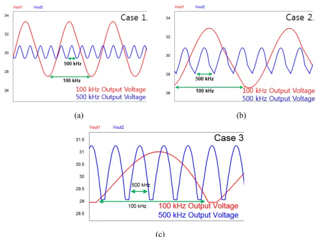
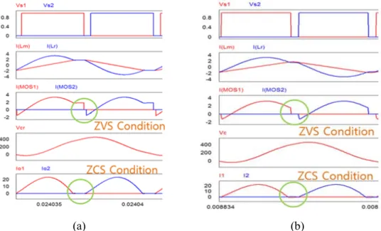
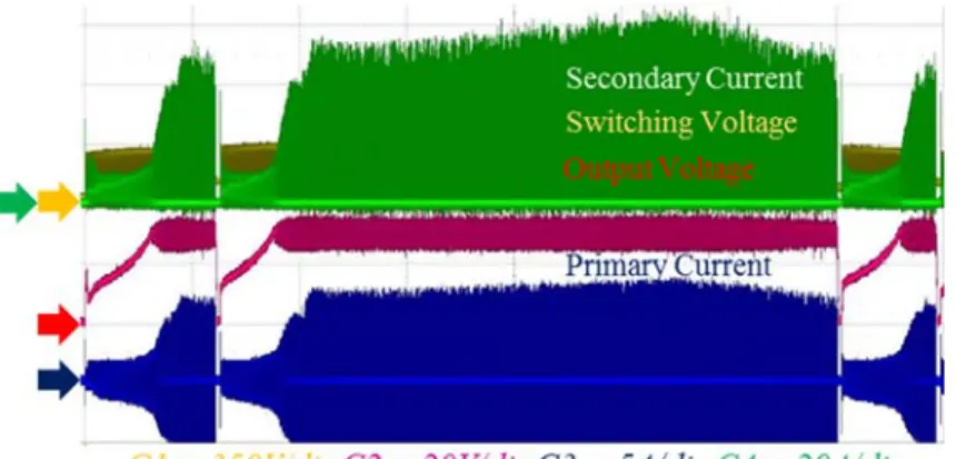
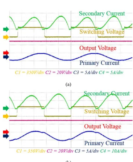
16 and 17 show the experimental waveforms at 100 kHz and 500 kHz switching frequency, which shows the operation of the power MOSFETs in the ZVS state and the secondary diodes in the ZCS state. Compared to operational waveforms at 100 kHz, operation at 500 kHz has high-frequency ringing in the current waveform caused by the influence of parasitic capacitance and stray inductance. Furthermore, the LLC high frequency resonant converter adopting smaller output capacitance and smaller ESR has an advantage of smaller output voltage ripple as derived in (5) and Fig.
To verify the variation of the relative stability according to the output capacitor, the high output capacitance case (6600 μF, 9 mΩ), as shown in Fig. As a result, the higher output capacitance makes the smaller output voltage variation according to load changes. Compared to the 100 kHz converter, the power conversion efficiency of the 500 kHz converter decreases by 2% at the nominal load, as shown in Fig.
This efficiency drop is the result of higher switching losses and higher hysteresis losses despite the soft switching techniques. Theoretical and experimental Bode plot of a small signal response of 500 kHz using high capacitance: (a) Theoretical Bode plot of the closed loop gain, (b) Experimental Bode plot of the closed loop gain. Step load response according to output capacitance: (a) Step load waveforms using small output capacitance, (b) Step load waveforms using high output capacitance.
Other passive components also have temperature rise, but the difference is less than the case of active and magnetic components.
Peripheral Circuit Design and Control Strategy for High Switching Frequency
- Side Effect of High Speed Switching
- High Speed Switching Characteristics of GaN E-HEMT
- Soft Start Algorithm for High Switching Frequency
- Simulation and Experimental Results with 1 MHz LLC Resonant Converter
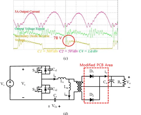
24 (c), the secondary side stray inductance produces high reverse voltage peaks on the secondary rectifier diode, which can be reduced by the short PCB path. In addition, the parasitic inductance in the gate driver produces unwanted spikes and rings that can induce overshoot or malfunction in the switching function of E-HEMTs. A reverse conduction voltage of GaN E-HEMT which is approximately 2.5V as shown in Fig.
In the case of the GaN E-HEMT, the high reverse bias voltage in the bootstrap driver must be compensated for the stable operation of the high-side switch as shown in Fig. Using a bootstrap diode that has a high forward voltage drop to the reverse conduction voltage of the GaN E-HEMT can compensate for the imbalance of the high side gate voltage. However, it cannot provide sufficient control bandwidth for the pulse frequency modulation (PFM) control method of the LLC resonant converter at 1 MHz.
In addition, the inverter requires a much higher switching frequency for the duration of the soft start to avoid inrush current at the beginning of the cold start. As a conventional LLC resonant converter soft-start algorithm, the switching frequency is reduced from twice the switching frequency of the rated operating frequency and reduced to the rated frequency for steady-state operation. The simulation results of the LLC resonant converter show the performance of the ZVS E-HEMT and the performance of the ZCS secondary diodes, which can reduce the switching losses.
Compared to 100 kHz switching frequency operation, the capacitance and inductance of passive components are drastically reduced at 1 MHz operation. The performance of E-HEMT under ZVS condition and secondary diodes under ZCS condition is verified with the proposed design. 35, the efficiency of a 1 MHz converter is lower than that of a 100 kHz converter due to higher switching losses.
Summary
Future Plan
Moon, “A New LLC Series Resonant Converter with a Narrow Switching Frequency Variation and Reduced Conduction Losses,” IEEE Trans. B, “A Very Low-Profile Dual Output LLC Resonant Converter for LCD/LED TV Application,” IEEE Trans. Jung, “Bifilar winding of a center-tapped transformer including integrated resonant inductance for LLC resonant converter,” IEEE Trans.
Kwon, "Transformer Design Methodology Including Integrated and Center-Tapped Structure for LLC Resonant Converters," Journal of Power Electronics, vol. Schetters, "Design of a 1-MHz LLC Resonant Converter Based on a DSP-Driven SOI Half-Bridge Power MOS- module,” IEEE Trans. Jung, “High Efficiency Isolated AC-DC Converter Using Three-Phase Interleaved LLC Resonant Converter Using Y-Connected.
Han, "Precise Analysis Solution for the Peak Gain of LLC Resonant Converters," Journal of Power Electronics, s. Blalock, "Evaluering af 600 V Cascade GaN HEMT in Device Characterization and all-GaN-based LLC Resonant Converter," i Proc. Lin, "Digital Compensator Design for LLC Resonant Converter," i Computer, Consumer and Control (IS3C), Internationalt symposium om, s.
Jee-Hoon Jung for the continued support of my study and related research, for his patience, motivation and vast knowledge.