Perspective
Characterizing the Efficiency of Perovskite Solar Cells
and Light-Emitting Diodes
Su-Hun Jeong,
1,8Jaehyeok Park,
2,8Tae-Hee Han,
3,8Fei Zhang,
4Kai Zhu,
4Joo Sung Kim,
1Min-Ho Park,
1Matthew O. Reese,
4,* Seunghyup Yoo,
2,* and Tae-Woo Lee
1,5,6,7,*
Metal halide perovskites (MHPs) are being widely studied as a light- absorber for high-efficiency solar cells. With efforts being made throughout the globe, the power conversion efficiency of MHP solar cells has recently soared up to 25.2%. MHPs are now being spotlighted as a next-generation light-emitter as well. Their high co- lor purity and solution-processability are of particular interest for display applications, which in general benefit from wide color gamut and low-cost high-resolution subpixel patterning. For this reason, research activities on perovskite light-emitting diodes (LEDs) are rapidly growing, and their external quantum efficiencies have been dramatically improved to over 20%. As more and more research groups with different backgrounds are working on these perovskite optoelectronic devices, the demand is growing for stan- dard methods for accurate efficiency measurement that can be agreed upon across the disciplines and, at the same time, can be realized easily in the lab environment with due diligence. Herein, op- toelectronic characterization methods are revisited from the view- point of MHP solar cells and LEDs. General efficiency measurement practices are first reviewed, common sources of errors are intro- duced, and guidelines for avoiding or minimizing those errors are then suggested to help researchers in fields develop the best mea- surement practice.
INTRODUCTION
Metal halide perovskite (MHP)-based optoelectronic devices have a great potential to compete with the well-established optoelectronic devices such as silicon (Si), gal- lium arsenide (GaAs)-based solar cells, and organic light-emitting diodes (OLEDs).
Three-dimensional (3D) MHPs have an ABX3 perovskite structure where A is an organic cation (e.g., methylammonium [MA] CH3NH3+, formamidinium [FA]
CH(NH2+), or an alkali-metal cation such as Cs+), B is a transition-metal cation (e.g., Pb2+), and X is a halide anion (Cl, Br, or I). The optical and electrical prop- erties of MHPs are easily tunable by substituting cations and anions. MHPs are solu- tion-processable semiconductors with unique optical and electrical properties due to the combination of a high absorption coefficient (CH3NH3PbI3: ~104cm1-105 cm1for photon energy ranging 1.5 eV–3.0 eV)1that is higher than that of Si and long carrier diffusion length. The photogenerated carrier profiles depend on the ab- sorption coefficient of the absorber, and the high absorption coefficient of MHPs, along with long carrier diffusion length, makes it possible to be thin, typically less 500 nm.2–4The fundamental origin of these unique electronic and photophysical properties have been found to be the unique atomic electronic configuration of
Context & Scale
Metal halide perovskite (MHP)- based solar cells and light-emitting diodes (LEDs) have shown a great potential to compete with the conventional optoelectronic devices such as silicon, gallium- arsenide-based inorganic solar cells, and organic LEDs. MHPs have been widely studied as a light- absorbing material for high- efficiency solar cells due to their high charge-carrier mobility and direct band gap leading to large absorption coefficient. Also, MHPs provide benefits of wide color gamut and low fabrication cost for display applications due to their high color purity and solution processability.
There are features specific to MHP- based solar cell and LED devices that make accurate measurement of their device efficiency challenging or at least tricky. In the context, optoelectronic characterization methods and common sources of errors are reviewed, and accurate measurement guidelines for device efficiencies in a viewpoint of MHP- based solar cells and LEDs are suggested. The guidelines would improve the reliability in the uprising research on MHP-based solar cells and LEDs, helping researches in the fields develop the best measurement practice.
Pb and symmetry of MHPs (the lone pair Pb 6s and the inactive Pb 6p orbitals, plus strong spin orbit coupling induced by its heavy atomic mass).5The conduction band minimum (CBM) of MHPs mainly forms from Pb 6p states, and the valence band maximum (VBM) consists of antibonding states of Pb 6s and I 5p orbitals. The unique combination of electronic and structural (symmetry) properties in MHPs renders not only direct band gap but also p-orbital-to-p-orbital optical transition (absorption), which is ideal for a good light absorber and light-emitter. From the electronic config- uration, MHPs also possess advantages of small effective mass for both hole and electron and less non-radiative recombination due to their defect-tolerant electronic characteristics, and therefore have an exceptionally long carrier lifetime (>1ms) and diffusion length (>1mm).3–5
In recent years, use of MHPs has been increasingly extended to the field of light- emitting diodes (LEDs). Their high color purity with narrow full-width-half-maximum (FWHM) of luminescence makes MHPs attractive for future display applications.6,7 Luminescence band shape can be generally related to the vibrational motion of crys- tal lattice and/or molecules of the electronic ground state and excited states (i.e., electron-phonon coupling).8Certain high-frequency molecular vibration modes in organic molecules result in strong electron-phonon coupling, which leads to a large equilibrium offset between ground and excited states, thereby broadening the emission and incurring a large Stokes shift.8For example, the molecular torsional mode of the conventional organic emitter N,N’-Bis (3-methylphenyl)-N,N’-diphenyl- benzidine (TPD) leads to a large Stokes shift and broad emission with Poisson pro- gression over an effective mode of 158 meV (Huang-Rhys factor, S:0.87).9The elec- tron-phonon coupling in MHPs, which mainly stems from longitudinal-optical phonon of metal-halide vibration mode (~60 meV, S:0.6),10is less than in organic luminescent materials, resulting in a smaller Stokes shift and narrower emission band width than those of organic materials used in OLEDs.8,10
The electroluminescence (EL) efficiency of perovskite LEDs (PeLEDs) has been dramatically improved in a relatively short period; the highest external quantum ef- ficiency (EQE) over 20% has been reached, which is comparable to those of phos- phorescent OLEDs.11–13
The certified power conversion efficiency (PCE) of perovskite solar cells (PeSCs) have reached 25.2%.14Accurately and precisely measuring the efficiency of solar cells is one of the basic procedures in photovoltaic labs worldwide. International certifica- tion labs serve as the custodians of the record efficiencies, which publish semi-annu- ally in Progress in Photovoltaics14and more recently have been compiled with detailed information in an interactive graph available online.15It is important, how- ever, for research and development labs to be able to measure similar values as a certification lab. While there is not an analogous certification infrastructure for LEDs, the same general principle applies of wanting comparable performance mea- surements between labs.
While the methods for characterizing PeSCs and PeLEDs may largely be taken from other portions of the wider (thin film) solar cell and (organic) LED communities, this does not mean that they are uniformly and well-practiced; furthermore, some of the material properties of perovskite optoelectronic devices require additional care when performing measurements. The ion migration and potentially related hysteret- ic effects in perovskite devices in particular can have strong effects on elements such as scan rate and sweep directions in both PeSCs and PeLEDs. In the case of PeLEDs, the optoelectronic measurement methods can be taken largely from those used for
1Department of Materials Science and Engineering, Seoul National University, 1 Gwanak-ro, Gwanak-gu, Seoul 08826, Republic of Korea
2School of Electrical Engineering, Korea Advanced Institute of Science and Technology (KAIST), 291 Daehak-ro, Yuseong-gu, Daejeon 34141, Republic of Korea
3Division of Materials Science and Engineering, Hanyang University, Seoul 04763, Republic of Korea
4National Renewable Energy Laboratory (NREL), 15013 Denver West Parkway, Golden, CO 80401, USA
5Research Institute of Advanced Materials, Seoul National University, 1 Gwanak-ro, Gwanak-gu, Seoul 08826, Republic of Korea
6Nano System Institute (NSI), Seoul National University, 1 Gwanak-ro, Gwanak-gu, Seoul 08826, Republic of Korea
7Institute of Engineering Research, Seoul National University, 1 Gwanak-ro, Gwanak-gu, Seoul 08826, Republic of Korea
8These authors contributed equally
*Correspondence:
[email protected](M.O.R.),
[email protected](S.Y.),[email protected](T.-W.L.) https://doi.org/10.1016/j.joule.2020.04.007
OLEDs16because their planar configurations are essentially the same. Nevertheless, some properties specific to PeLEDs can make the measurement more prone to er- rors. For example, much narrower EL spectra inherent to PeLEDs can render their angular characteristics to be different from that of Lambertian,17,18which has often been assumed for bottom-emission-type OLEDs having a no- or low-microcavity ef- fect. Different ratios of the current efficiency (CE) to EQE values reported, even for the identical device geometry combined with the same emitters, suggest that there are group-to-group variations in treating the angular spectral characteristics in their EQE estimation. Hysteretic behavior is also an important factor that can make it tricky to precisely characterize the metrics of both PeSCs and PeLEDs, although ion migration may be exploitable in memristors and synapse-mimicking de- vices.19,20Effect of parameters like scanning rate and bias-sweep direction must be taken into account carefully.17,21Of course, it will also be important to identify the material set and device architectures that are relatively robust against hystere- sis.22As the efficiency records of PeSCs and PeLEDs are continually increasing over time, it is essential to establish standardized guidelines to characterize effi- ciencies for both PeSCs and PeLEDs. Here, we first present a brief introduction to efficiency measurement methodologies for PeSCs and PeLEDs along with definition of key terms and discussion on common sources of errors in perovskite-based de- vices. We then suggest practical guidelines for avoiding or minimizing those errors to ensure precise estimation of the efficiencies in those devices.
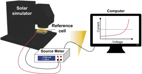
CHARACTERIZING THE EFFICIENCY OF PEROVSKITE SOLAR CELLS Three pieces of equipment are required at minimum for reasonable quality measure- ments: a solar simulator, a quantum efficiency (QE) measurement tool, and a cali- brated reference cell (Figure 1). A fourth piece of equipment, a spectrometer to cap- ture the lamp spectrum, is required for the highest quality measurements. This section of the paper will describe our view on the equipment, considerations, and procedures to encourage accurate and precise efficiency measurements for hybrid perovskite solar cells in a manner accessible to R&D labs.
Characterization Tool: Solar Simulator, Quantum Efficiency Measurement Tool, Reference Cell
Solar Simulator
To begin, solar cells are measured in relation to a standard reference spectrum with standard test conditions. For non-concentrating or tracking terrestrial applications,
- +
- 0.002 mA + 1.00 V
Source Meter
Computer Solar
simulator
+ + + + + + + + + + + + + + - +
- +
-
Voltage
Current
Reference cell
Figure 1. Schematic Illustration of PCE Characterizing Methods for PeSCs
the reference spectrum is AM1.5G (Figure S1A).23The ‘‘AM’’ stands for ‘‘air mass’’
and 1.5 is how many thicknesses of the atmosphere have been traversed; one is tra- versed when the incident light travels normal to the atmosphere. The ‘G’ stands for global tilt—used to account for ‘‘flat plate’’ (i.e., systems intended to operate at 1 sun). In this spectrum, there are both direct and diffuse components compared to AM1.5D, which is solely the direct portion of the spectrum, which is appropriate for concentrating systems that must track the sun’s motion, because as concentra- tion levels increase, the collection angle of light is limited, which decreases the contribution of the diffuse component. While the reference spectrum is somewhat arbitrary, as the spectrum even at a single location changes with time, it is meant to simulate a mid-latitude spectrum (e.g., the United States) around noon on a clear day. For the interested reader, a nice solar spectrum calculator found online can be used to illustrate the variations.24While somewhat arbitrary, the reference spectrum has very important effects on final measurements as will be seen below. Standard test conditions (STCs) specify an irradiance of 1 sun to be 1 kW m2 (100 mW cm2), which tends to be present at most locations only on a sunny day around noon, as well as a nominal operating cell temperature of 25C. While 25C is close to room temperature, cells can heat up quickly to much higher than this value (>40C is readily possible) without some sort of active cooling (e.g., a fan or wa- ter-cooled plate) integrated into a solar simulator. The choice of these conditions can be understood, in addition to the appealing roundness of the numbers, because most solar cells (c-Si especially) are more efficient at lower temperatures and higher intensity solar irradiance.
Solar simulators are typically sold with a three-letter class system. In order, they indicate the quality of the spectral match, spatial uniformity, and temporal stability.
Table S1defines what classes A–C mean for each type. The spectral quality is often the biggest focus of many groups. To understand this,Figure S1A shows a represen- tative spectrum of a class A spectrum xenon-lamp-based simulator with its AM1.5G filter set compared to the actual AM1.5G reference spectrum. To establish that this spectrum is indeed class A, after measuring the simulator’s spectrum, one would integrate the irradiance of 100-nm-wide bins from 400–900 nm and one 200-nm- wide bin from 900–1,100 nm of the simulator and compare it to the integrated values for the reference spectrum. To be a class A spectrum requires that each bin be within G25% of the integrated reference spectrum. While a simulator’s class is defined by its worst bin, a bin may have regions that are significantly lower or higher irradiance than the bin’s average. This binning with integrated irradiance thereby makes the spikes associated with many lamp spectra acceptable. Furthermore, irra- diance values are unspecified at <400 and >1,100 nm. Simulators that have a bin worse than class C are sometimes specified as class X. It is possible to generate a relatively inexpensive solar simulation source from a lightbulb that is technically a class X simulator but has high quality matching in the region of interest to higher band-gap technologies.25It is also worth noting that purchasing a simulator of a particular class (e.g., AAA) should be able to achieve its designated class; however, if it has not been calibrated, it is typically not performing at this level. Lamp spectra can vary with time, although manufacturers often try to take this into account when designing their filters over a specified lamp life. More significantly, whenever a bulb is changed, the spatial uniformity must be recalibrated. According to International Electrotechnical Commission (IEC) 60904-9,26 the spatial uniformity should be measured in a minimum grid of 838 points across the designated area. This can be done by moving a small area Si cell held parallel to the measurement plane, although more sophisticated apparatuses exist as well, including multiple diode ar- rays or cells on motion stages. It is worth emphasizing that the spatial uniformity
specification is over a designated area. Many groups have simulators with much larger designated areas than their test cells. To minimize the effects of spatial unifor- mity, two approaches can be taken. The most straightforward is to measure each cell in the exact same location—if multiple cells are on a substrate, the substrate is shifted between measurements. The second approach is to measure substrates in a fixed location relative to the lamp and calibrate the relative variation between cell locations on the substrate. In the event that a cell is larger than the uniformity, other methods can be used.27Changes in irradiance with time (temporal stability) are often associated with the power supply and bulb age (older bulbs may start be- ing unstable). To remove these variations, a monitor diode can be measured simul- taneously over the course of an efficiency measurement of a test cell. This can then establish if the irradiance during a particular measurement was, for example, 1.01 sun. Assuming linearity (which can be measured for a particular cell or configuration), the measured current can then be renormalized back to a 1-sun value.
Standard test conditions dictate that efficiencies should be at 1-sun intensity. This is typically established in the case of simulators with divergent sources by adjusting the separation between the lamp and sample. For simulators with collimated sources, the intensity is relatively constant with separation, so instead the lamp power is adjusted to achieve 1-sun intensity, which may be maintained by feedback to a monitor diode. While this can achieve a fairly constant irradiance, the spectrum can shift somewhat with lamp power changes. A simulator is set to its 1-sun intensity immediately prior to sample measurement using an appropriate reference cell (dis- cussed below) by making adjustments to the simulator as appropriate to achieve the 1-sun short-circuit current of the reference cell.
It is well-known that changing the irradiance can lead to different recombination dy- namics as the open-circuit voltage increases logarithmically with the ratio of photo- current to dark (recombination) current. Fill factor has a more complicated relation- ship, with potential changes in series and shunt resistance, as well as ideality factor.
This is why the highest reported efficiencies have been at high concentrations for III- V cells.6In the absence of complications with keeping cells at constant temperature and series resistance losses from joule heating, solar cells should ideally be more efficient at higher irradiance with higher VOCmeasured. Altering carrier dynamics (e.g., the onset of bimolecular recombination), however, can lead to a reduction in fill factor with increasing irradiance. Since there is an optimum concentration value for each cell, standard test conditions should be performed as close to 1 sun as possible rather than an arbitrary intensity and then normalizing to 1 sun. This allows a direct comparison within a technology as well as between technologies.
Quantum Efficiency Measurement Tool
The external QE of a solar cell is a measure of the likelihood of whether photons of a particular wavelength can be harvested and converted to current. This ultimately is used to establish the spectral responsivity of a cell.Figure S1B shows several QEs of different band-gap perovskite cells. Some groups use a purchased turn-key system for this; others will make their own using a monochromator, chopper, lock-in, pre- amp, and reference cell. While many will do a ‘‘dark’’ QE measurement in which the only intentional light incident on the cell is the very weak, monochromatic light (< 0.01 sun), a white-light-biased measurement is preferable, in which a ‘‘DC light biases the cell closer to realistic operating conditions, with the chopped monochro- matic light representing only a small perturbation. This means that what is actually measured is a differential spectral responsivity rather than a direct spectral respon- sivity. Samples measured without a light bias can artificially be affected by trap
states, which a light bias can readily fill.28,29Similarly, surface passivation can be wavelength dependent.28‘‘Well-behaved’’ cells might be considered only modestly non-linear over a wide range of intensities without great sensitivity to chopping fre- quency—although it is worth noting that DC bias light can mitigate low response times.29Furthermore, non-linearity by itself is not an exceptional case for solar cells with even Si cells documented to exhibit non-linearities.28,30Sublinear behavior can occur for a number of reasons including field dependent charge collection, which collapses with increasing irradiance and decreasing diffusion lengths.28,30Inten- sity-dependent QE has also been used to study recombination mechanisms (e.g., bimolecular recombination, field effects, and contact layers) and even correlate them with fill factor.31Supralinear behavior can be observed for cells in which the se- ries resistance limits Jsc.30Edge effects have been correlated to both sub- and supra- linear behavior.30While dark QE can lead to errors as large as 100% in Jsc, the lowest error is counterintuitively obtained at irradiances less than 1 sun.30For samples that are non-linear, the non-linearity can be represented as JSC= c3Ig, where I is the irra- diance, c is a constant, andgis a measure of the non-linearity (g= 1 is linear). The formula JDC Bias=gg/(g1)JSC, 1 suncan be used to calculate the correct bias light irra- diance as measured by the measured device current density (JDC Bias). For mildly non-linear behavior (i.e., 0.9 < g < 1.1), this minimum in error corresponds to EQE measurements performed with a light bias of ~1/e of the 1 sun irradiance.30 For devices with much greater non-linearity, the bias light intensity should be adjusted to minimize the error.
EQE is a measure of the fraction of the incident photons that are converted to photocurrent, whereas internal quantum efficiency (IQE) is a measure of the fraction of absorbed photons that are converted to photocurrent. In general, QE (EQE or IQE) can be affected by light harvesting and charge collection, depending on the actual materials and structures used in a device stack. The non-ideal QE can thus be attributed to optical loss and/or electrical loss. The optical loss primarily consists of the loss from reflection and parasitic absorption from various transport or contact layers. In a study32 using 1.55-eV perovskite absorber as an example, detailed modeling coupled with experimental data shows that the maximum Jsc(27.23 mA cm2based on the 1.55-eV band gap) can be reduced to 21.61 mA cm2from the reflection loss of 2.48 mA cm2 (9.1%) and parasitic absorption loss of 3.14 mA cm2(11.5%) from transparent conducting oxide (TCO) and the contact layers. Using an antireflection coating is a common way to reduce the reflection loss—reducing reflection losses by more than ~3%–4% absolute over a wide wavelength range is challenging.33The parasitic absorption loss can also be reduced by using thinner transport layers or using alternative materials with less absorption in the spectrum range relevant to the absorber layer. Electrical loss primarily results from surface recombination at front or back contacts, short diffusion length associated with poor transport and/or carrier lifetime, and resistive loss from series and shunt resis- tances. In the same study,32it was shown that the electrical loss could account for 17.7% loss of the power output. It is worth noting that the electrical loss is related to charge collection, which could be affected by the voltage bias conditions. Thus, QE should be measured at short-circuit condition to avoid voltage-bias-induced current, especially for low-quality devices.
For QE measurement, it is worth noting that the chopping frequency should be slow enough to not affect charge collection and not be at the power line frequency or a multiple thereof (prime numbers are a good choice; e.g., 37 Hz). The DC light source may be at the line frequency and does not need to have a class A spectrum. Both absolute and relative QEs can be measured. An absolute QE (e.g., the different
band-gap perovskite cell QEs inFigure S1B) requires that the entire beam from the system be focused within the device area, such that a known intensity is striking the sample. A relative QE uses a larger spot than the sample, as in the Si reference cell QEs shown inFigure S1B. Measuring the QE yields not only important information about a device’s behavior (e.g., absorption depth, optical losses, band gap), but it is also used to establish the spectral mismatch factor and, in the case of an absolute QE, can be integrated to verify current-voltage (IV) measurements.34When report- ing results, QE and IV data of thesame cellshould be presented together rather than cherry-picking ‘‘representative’’ data. This is especially important for perovskite systems in which the composition and hence band gap may be somewhat altered between samples.
Calibrated Reference Cell
A calibrated reference cell with known QE and 1-sun current is also required for solar simulations. For a group focusing on research at a single band gap, the reference should have as similar a band gap as possible. For a group exploring numerous band gaps, either multiple reference cells should be used or an Si reference with multiple filter sets should be employed. A reference cell should be in a package that is light impervious such that no stray light will reach the side or back of the refer- ence. A reference cell should be stable over time. Even Si reference cells are techni- cally supposed to be recalibrated once a year. One of the certification labs can be used for this service. Similarly, a reference cell for QE measurements is important.
Avoiding Measurement Discrepancy and Errors Spectral Concerns
Once a user has representative QE information about the cell under test, the refer- ence cell, and the lamp spectrum, a spectral mismatch factor may be determined.
First, the QE,hQE, is transformed into a spectral responsivity,S, usingEquation 1, SxðlÞ=ql
hchQE;xðlÞ (Equation 1) where the subscript,x, is used to indicate if the QE is from the reference cell or test cell,qis charge quantity,his Planck constant, andcis the speed of light in vacuum.
Then, a series of four convolutions are performed to balance the currents that would be measured by either the reference cell or test cell under either the reference spec- trum or lamp spectrum (represented as Ix,ybelow) to calculate the spectral mismatch factor,M,
M= Rl2
l1ERefðlÞSRefðlÞdl Rl2
l1ERefðlÞSCellðlÞdl Rl2
l1ELampðlÞSCellðlÞdl Rl2
l1ELampðlÞSRefðlÞdl=IRef;1 sun
ICell;1 sun
ICell;Meas
IRef;Meas
(Equation 2) whereERef is the irradiance of the reference spectrum (e.g., AM1.5G),ELampis the irradiance of the lamp,SRefis the spectral responsivity of the reference diode, and SCellis the spectral responsivity of the test cell. These four integrals are presented graphically inFigure S3to try to illustrate what the spectral mismatch factor is doing.
This is adapted from a recent book chapter, which has an expanded discussion.35 The change from QE from spectral responsivity is illustrated, as well as the effect this has with the integrated spectrum. A cell has an increasingly weighted response to photons near its band edge. This is important to consider when choosing a refer- ence cell for a particular test cell. The spectral mismatch correction has the greatest influence on the current (i.e., Jsc), with a correction being directly applied to each current point in the current-voltage curve. This has a second order effect on the fill factor, with generally very limited changes to the open-circuit voltage. Even though
a cell exhibits significant wavelength dependence over its collection range, class A spectra tend to minimize voltage effects.
Before using a simulator, a user will typically set the 1-sun intensity based off their reference cell’s known calibrated current (ICell;Meas). This value is how much current the reference should generate under the reference spectrum. In doing this, two of the integrals should cancel one another (reference spectrum*reference cell and lamp*reference cell). When the test cell is measured, ICell;Meas is represented by the integral of lamp and test cell. This needs to be transformed into the current that would be produced if the test cell were exposed to 1-sun intensity under the reference spectrum (the last integral,ICell;1 sun). To transform the measured current under the lamp spectrum, one simply takes the measured cell current and divides byM(assuming that the simulator was actually set to exactly 1-sun intensity on the reference diode).
Ideally,Mshould be as close to unity as possible. In examining the integrals, one sees that there are two hypothetical ways to guarantee a mismatch factor of unity.
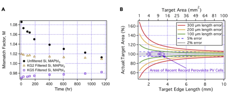
One is to have a lamp spectrum that is identical to the reference; the other is to have a reference cell with identical spectral response to the test cell. In reality, neither will be possible. While having a well-matched (i.e., class A) spectrum is a good start to minimizing spectral errors, by itself it is not enough. Some researchers put an excessive amount of value in the spectral class of a simulator and then pay lit- tle attention to making sure they have a reference cell that has a similar spectral response to their test devices. A poorly matched reference cell will respond to different (extra or fewer) portions of the lamp spectrum than the test cell, making the measurement more sensitive to differences between the lamp and reference spectrum. This is illustrated inFigure 2A, where MAPbI3is compared to an unfiltered Si reference cell (a poor choice). In general, it is significantly less expensive and easier to have a reference cell that is well-matched to the test cell than matching the lamp to reference spectrum (remember class A means G 25% integrated mismatch per spectral bin). The easiest way to do this for any technology is to have a stable, packaged representative cell certified and use this as a reference. If possible, a group can make and package one of their cells for measurement by a cer- tification lab and use it on occasion for calibrations. The next best way for groups that might want to explore different band gaps is to have a packaged Si reference cell
A B
Figure 2. Spectral Mismatch and Length (Area) Concerns
(A) Spectral mismatch factor, M, versus time calculated for a Si reference cell with either no filter, a KG5, or a KG2 filter relative to a MAPbI3cell for a class A filtered xenon-lamp-based solar simulator.
(B) Length (area) errors calculated for a square cell with a side of target length. These errors can begin to dominate other sources with even minor (mis)measurements. Recent perovskite records have all been for small area cells, illustrating the importance of area measurement.
calibrated with a series of bandpass filters. Some representative filters and what they do to an Si cell are shown inFigure 2A; inexpensive bandpass filters (e.g., Schott Glass BG- or KG-series colored glass filters) can be appropriate for standard perov- skite band gaps. GaAs references can also be purchased, which are relatively well matched to MAPbI3. It is worth noting that reference cells should ideally be pack- aged in a manner that will minimize backside collection, reflections, and light piping (waveguiding through a substrate to a device).
For the best measurements, the lamp spectrum at the time of the measurement should be known. Lamp spectra can change over a bulb’s lifetime. In the case of pop- ular xenon arc lamps, this is a result of deposition of the electrode over time onto the quartz envelope of the lamp as a thin layer screens out short (blue) wavelengths.
Initially, the lamp will uniformly pass the generated light. Over time, the lamp spec- trum transitions from being blue rich to red rich. Measuring the lamp spectrum al- lows the diligent user to measure these shifts. In the case of inappropriate choice of a reference cell (poorly matched spectral response), the changing lamp spectrum for even good simulators can result in large shifts in the spectral mismatch factor,M (Figure 2B). Careful choice of the reference cell can mitigate this effect. For reason- ably good measurements, having representative early-life and end-life spectra of the lamp can allow a group to establish the limits of this effect, although it is worth noting that different bulbs and different filter sets from the same manufacturer can result in somewhat different spectra (Figure S3). This information should be used to inform the potential magnitude of spectral errors rather than trying to ascribe ab- solute values. It is worth noting that measuring the lamp spectrum in well-calibrated units of W m2nm1requires carefully calibrating the spectrometer. Typical inex- pensive USB spectrometers out of the box have well-calibrated wavelengths, but not intensity.
These spectral shifts also can have important implications on stability measure- ments. Apparent changes in efficiency can be either masked or exacerbated, with bulb changes leading to abrupt shifts in data. While xenon-arc bulbs are well-loved by scientists seeking a class A spectrum, spectral sensitivity on stability is hard to know for a technology that is rapidly exploring changes to not only its absorber formulation but architecture. Likely, if intensity is being monitored with an appropri- ately matched reference cell, the spectral changes over a single lamp’s lifetime will have minor effects on stability. Some may choose to use alternate light sources that might be cheaper and/or more stable over time (e.g., metal halide, sulfur plasma, or LEDs), but ultimately there is not a single ‘‘correct’’ source because the spectral sensitivity on stability is not well understood. In practice, each architecture will have to be individually examined. It should be noted that UV-rich or -poor light sour- ces may play a role in certain systems (e.g., transport layer trap filling and/or photo- catalytic behavior). The authors are unaware of clear evidence that can balance the effects generally for perovskite systems of spectral match, spatial uniformity, and temporal stability—setting up stability systems is always a compromise of these three aspects because cost plays a role over long times and large areas. Following recommended practices like those proposed by Reese et al. for the organic photo- voltaic community,36in which a minimum of information always accompanies stabil- ity measurements including the lamp spectrum, can at least help the community un- derstand the measurement conditions.
Area Concerns
Perhaps most surprisingly, one of the biggest sources of errors historically in measuring emerging photovoltaic technologies has been associated with what
should be straightforward for all labs: area measurement. Research groups tend to make small cells for a variety of reasons including lack of uniformity, pinholes, at- tempting to get larger current densities and fill factors through poorly optimized front contacts, and the desire for statistics on small substrates (25325 mm2). There are several approaches to cell layouts. One uses a ‘‘crossbar’’ geometry in which there is a patterned transparent contact, and a metal contact is evaporated through a shadow mask. In this case, the cell area should be the overlap between the trans- parent and metal contact.
However, it has been shown that conductive transport layers can lead to large (>60%) errors for small devices37from collection outside of the metal and trans- parent contact overlap region. Other groups will create ‘‘island’’ back contacts on an unpatterned transparent contact. This addresses collection from a conductive transport layer in contact with the transparent contact, but not from any conductive layers at the back. Additionally, it is worth noting that many groups who use shadow masks do not measure the area of a device each time, but rather assume that the metal area is well known. Shadow masks lead to imperfect edge definition with the potential for tens of microns to >100-mm spillover at each edge.
Furthermore, the opening of the shadow mask changes in size with the buildup from many depositions. Rotating a substrate during the deposition tends to improve the contact but exacerbates area definition problems. Even using a calibrated optical microscope to measure the area of a sample with shadow mask deposited contacts can lead to discrepancies for the location of a metal edge—different users may make different judgement calls that can result in >100-mm differences in lengths. Further- more, it has been demonstrated that when laterally conductive transport layers are utilized, carrier collection can occur millimeters away from the metal contact, but even when low lateral conductivity transport layers are used, significant collection can still be observed hundreds of microns away from the metal’s edge.37
Figure 2B highlights the potential error associated with small area devices that do not have carefully defined areas with some of the more recent device areas for certi- fied record perovskite cells. For samples that are not ‘‘mesa isolated’’ (one contact and absorber is etched down to the other contact), an ‘‘aperture’’ is used to define the device area during the efficiency measurement. The aperture is typically a thin (opaque) metal sheet with openings that have well-known areas. The metal sheet will extend past the edge of a sample to make sure that no waveguiding occurs in the substrate. A standard, rigid aperture is preferable to a custom aperture from something like vinyl (e.g., electrical) tape, as such tapes can stretch and form curved edges. For small area devices (<1 cm2), an aperture is required for certified measure- ments. To establish if the designated area of a device is correct for an unapertured measurement, its current density can be compared to that of a measurement with an aperture. It is worth noting that in all cases, an aperture will necessarily lower the open-circuit voltage and alter the fill factor. Kiermasch et al. provide a mathematical framework of how this will affect device performance when temperature effects are ignored,38demonstrating that changes in voltage can be on the order of 100 mV. As historically current density has been the largest discrepancy between labs, apertures will remain necessary so long as the community measures small devices. However, changes in open-circuit voltage are often deeply tied to the science limiting device performance, whereas current is often more related to engineering optical transmis- sion and absorption. This makes it worth measuring samples with and without apertures.
Current-Voltage Considerations: Hysteresis, Stable Power Output, Dynamic Current-Voltage
Finally, how to obtain the actual efficiency value of a PeSC has become a problematic issue since the first report of the strong hysteresis effect by Snaith et al.18For conven- tional solar cells, such as Si, CIGS, CdTe, the current-voltage (I-V) scan is commonly used to determine the PCE. However, the efficiency calculated from I-V scans for a perovskite solar cell could depend on the scan direction (i.e., reverse scan, where the bias is changed from open circuit to short circuit, or forward scan, where the bias is increased from short circuit to open circuit) and scan rate (i.e., how fast the bias voltage is changed during I-V scan).Figure S4A shows an example of the IV curves with both forward and reverse scans. The data were adapted from Kim et al.39In this example, the reverse scan yields a PCE of 19.7%, whereas the forward scan yields a PCE of 17.4%. The difference between these two PCEs with respect to one of these two PCE values (e.g., from reverse scan) is often used to describe the degree of hysteresis.40However, it should be noted that the degree of hysteresis can be strongly affected by the scan rates and thus should be used with care for com- parison. Extensive efforts have been devoted to studying the underlying mecha- nisms contributing to the hysteresis, such as ion migration, charge extraction, ferro- electric behavior, capacitance, etc.41–48Impedance spectroscopy has become an effective method to study the impact of bulk and contact on the hysteresis behavior as well as the device stability in recent years.49,50Although this large hysteresis behavior of perovskite solar cells presents an unprecedented opportunity to study various interesting physical behaviors, it nevertheless presents a significant chal- lenge for accurately determining the PCE based on the conventional IV scan. A rec- ommended practice is to conduct the stable power output (SPO) near the maximum power point (MPP). An example of the SPO measurement is shown inFigure S4B for the same device shown inFigure S4A. This is normally done by biasing the device near the maximum power voltage and monitoring the current density output to sta- bilize, which can then be converted to the power output or the conversion efficiency.
Because this measurement normally lasts for a few minutes with stable power output, it is generally accepted as a reliable way to verify or determine the PCE for devices with hysteresis. It is worth noting that a single measurement of SPO does not neces- sarily yield the maximum power output since the bias voltage is pre-determined or estimated using an IV scan. A more rigorous way is to conduct a series of SPOs over a range of bias voltages that will likely cover the MPP; the maximum PCE of this device will be determined by analyzing the voltage dependent SPOs.51This approach is similar to another method often called a dynamic, or asymptotic, IV. In the dynamic IV measurement, the device is scanned across the entire voltage range as in the con- ventional IV measurement with the device being held at each voltage step long enough to obtain the stabilized current output.52 This asymptotic method has been adopted by accredited cell calibration labs such as NREL and Newport. A key criterion for this method is that the measured current is determined to be un- changing at the 0.05%–0.1% level. The measurement of SPOs or dynamic IV often takes a much longer time (e.g., minutes to tens of minutes) than that for the conven- tional IV measurement (e.g., seconds). Thus, the stability of the devices under the ef- ficiency testing conditions becomes important and could be a significant challenge for certain types of devices. It is important to note that stable power output measure- ments should not be confused with measurements of long-term stability, which are beyond the scope of this paper. Measurements of long-term stability can be influ- enced by a variety of factors including load conditions (e.g., open circuit, short cir- cuit, maximum power point), nominal operating cell temperature, ambient, fre- quency of measurement, and other measurement conditions. Typically, for these sorts of experiments, solar simulator requirements are relaxed due to the cost of
maintaining high spectral quality uniform light sources. Actual stability, with respect to light soaking on the scale of hours or more and shelf life for the scale of weeks, while desired by certification labs, is not required for record efficiencies at present.
It is required, however, for the technology to advance.
Qualification and safety standards exist for commercial photovoltaic (PV) technolo- gies (IEC 61215, 61730), with technology-specific variants for 61215. At present, there are no perovskite-specific standards, although there is an IEC working group (IEC TC82 WG2) that is actively discussing this. The perovskite community has largely followed the International Summit on Organic and Hybrid PV Stability (ISOS) consensus protocols as a framework to both age and report stability results,36 which has a three-tier system for each aging type (e.g., ambient shelf life, heat, and damp heat for the different levels of dark storage). A recent update expands this framework beyond dark storage, light soak, outdoor, and thermal cycling to include light cycling and voltage bias tests, as well as formalizes an inert ambient variant for each type of test. The ISOS tests minimize the number of suggested conditions (e.g., ambient, 65C, or 85C) to facilitate comparisons between labs while providing vary- ing levels of severity.53
Photovoltaic Error Comparison
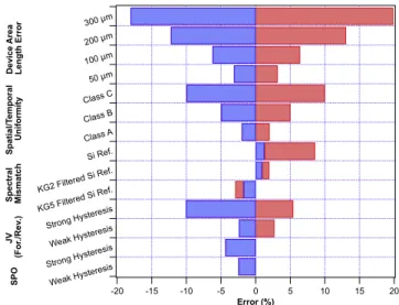
The text above details many well-understood aspects of photovoltaic efficiency characterization that should be considered by the careful practitioner. To graphically compare the relative magnitude of these errors, a tornado plot was prepared forFig- ure 3. Some portions have definitional maximum errors such as the spatial and tem- poral errors associated with different class simulators. It should be understood that these particular errors are worst case scenarios, and methods potentially exist to
-20 -15 -10 -5 0 5 10 15 20
Error (%) 300 µm
200 µm 100 µm 50 µm Class C Class B Class A Si Ref.
KG2 Filtered Si Ref.
KG5 Filtered Si Ref.
Strong Hysteresis Weak Hysteresis Strong Hysteresis Weak Hysteresis Spatial/Temporal UniformityDevice Area Length ErrorSpectral MismatchJV (For./Rev.)SPO
Figure 3. Tornado Plot of Standard Errors in PV Cell Efficiency Measurement
The device length error assumes a device area of 0.1 cm2with sides of actual length 3.16 mm. Each side is assumed to be longer or shorter by the length shown on the y axis. Spatial/temporal uniformity applies the maximum definition of spatial and temporal errors for different class simulators. Spectral mismatch error compares a MAPbI3cell to representative spectra from a new and older class A spectrum xenon lamp to different reference cells. The JV (For./Rev.) illustrates efficiency errors as measured relative to the asymptotic method for a device with strong hysteresis and one with weak hysteresis for various scan rates in the forward and reverse conditions. The stable power output (SPO) method illustrates efficiency errors for the same devices measured 20 mV off the Vmpp. Devices measured via the SPO method at Vmppyielded the same value as the asymptotic method.
reduce the errors as described above, such as introducing anin situmonitor diode to renormalize for temporal fluctuations.
The other errors, however, required choosing specific cases, so should be under- stood as illustrative, not absolute. Area errors can be quite large for small devices, which are generally being used in the perovskite community. Using the incorrect area for a 0.1 cm2device can easily become the largest source of error, which helps explain the community’s insistence on apertures when measuring small devices. The effect of spectral mismatch on even a class A spectrum can also be quite large and lead to overstating efficiency when using an improperly matched reference (here, for a MAPbI3 cell). For the efficiency measurement approaches, the asymptotic scan method, which is used by NREL’s certification group, is used as the zero-error case. Forward and reverse current-voltage scans are shown to be a plausibly large source of error depending on the level of hysteresis displayed by the device and scan conditions. It was found for both devices that the stable power output method agreed with the asymptotic method for the maximum power, but being off by as little as 20 mV could lead to sizable underestimation of the efficiency. The details of the measurements and device data are available inFigure S5andTables S2andS3.
CHARACTERIZATION OF ORGANIC AND PEROVSKITE LIGHT- EMITTING DIODES
Definition of Key Radiometric and Photometric Parameters and Their Relationship
In evaluating the performance of any light source, it is important to understand the difference between radiometric and photopic quantities. Radiometric quantities are the actual physical quantities related to the energy carried by light. In contrast, a photometric quantityXLcorresponding to a given radiometric quantityXRis ob- tained by weighting the spectral density ofXRat the wavelength ofl[=XR(l)] with the photopic response function V(l); i.e., the daylight human eye sensitivity as follows:
XL=KV
Z
XRðlÞVðlÞdl=KVXRðtotÞ Z
rðlÞVðlÞdlhKVXRðtotÞgV (Equation 3) whereKVis the conversion factor given as 683 lm/W,rðlÞis the spectrum of the light source normalized such thatRrðlÞdl=1 andgVhRrðlÞVðlÞdl; i.e., the overlap inte- gral betweenVðlÞandrðlÞ. Note that, in this formalism,XRðlÞ=XRðtotÞrðlÞ; where XRðtotÞhR
XRðlÞdl. The introduction of the normalized spectrumrðlÞcan be useful because spectral measurement can be done on a relative scale, not absolute.
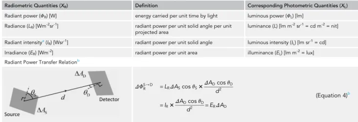
Radiometric quantities include radiant power, radiant intensity, irradiance, and radi- ance, and their corresponding photopic quantities are luminous power, luminous in- tensity, illuminance, and luminance (seeTable 1for definition and units of the radio- metric and photometric terms and their use in radiant power transfer relation between a source and a detector).
The photometric conversion given byEquation 3stems from the definition of the unit
’’candela’’ (cd)—one of the seven basic SI units—wherein 1 cd is given as the lumi- nous intensity of a source emitting, in a given direction, the monochromatic radia- tion of 1/683 W sr1with the frequency of 540 THz.54Note that this optical frequency corresponds tolof 555.017 nm whereVðlÞis peaked. By definition, cd is equivalent to lm sr1, andVðlÞis normalized such that its peak value is given by the unity so that the values in the other wavelength are given in a relative scale with respect to the value at the peak wavelength. This explains the origin that the luminous efficacy
KVis given by 683 lm W1and that the photometric conversion involves the overlap integral shown inEquation 3. It is also noteworthy thatVðlÞis the function estab- lished by Commission Internationale de l’E´clairage (CIE) and equalsyðlÞ—a color matching function used in CIE 1931 color space.55The tabulated values forVðlÞ are provided inTable S4.
Electroluminescence Efficiency
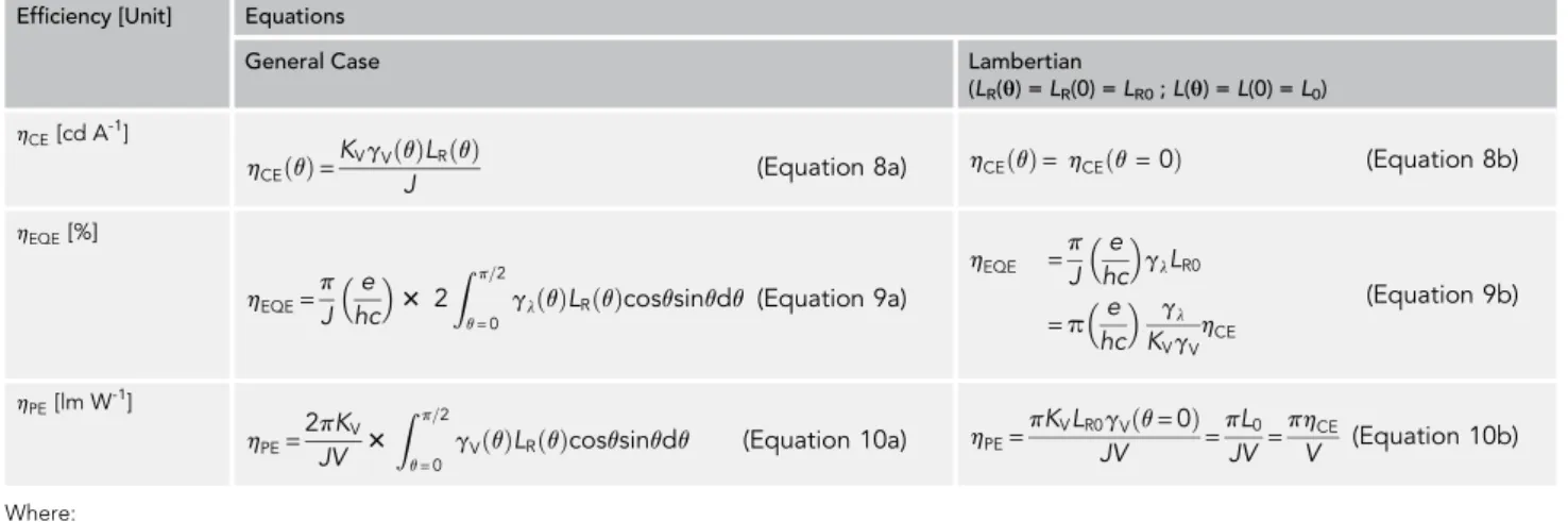
The EL efficiency is a performance parameter of prime interest for any LEDs. It includes current efficiency (hCE[cd A1]), EQE (hEQE[%]), and power efficiency (hPE [lm W1]) as defined inTable 2.16As PeLEDs are made in the form of a thin-film device like OLEDs, their EL efficiencies are determined only with the photons emitted into the upper hemisphere (i.e., photons emitted backward and sideways are not accounted for, as they do not contribute to the generation of light in forward direction).
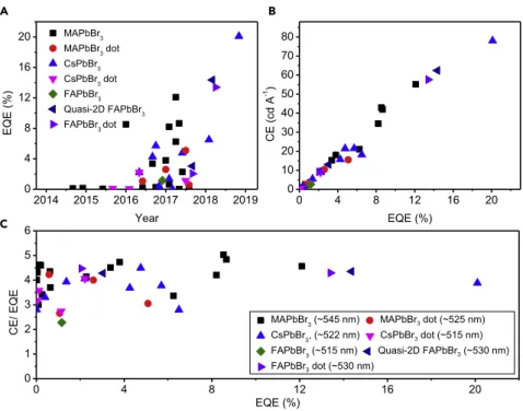
We have conducted a thorough literature search to illustrate the evolution ofhCE and hEQE of green PeLEDs (Figure 4A and Tables S5–S7). The EL efficiency of PeLEDs has dramatically improved by engineering of interfacial layers,7,56–60 electrodes,61,62perovskite film morphologies,63–71stoichiometry of precursors,63,72 dimensional control,73 and additives.63,74–80 Recently, perovskite dots with ligands have been developed to effectively confine excitons in perovskite nano- crystals,81–92 and the hCE and hEQE for red emission were increased up to 11.6 cd A1and 21.3% (hEQEestimated from an angle-dependent measurement), respectively.13 The high EQEs >20% were also obtained for near-infrared (NIR) emission from quasi-2D and 3D perovskite emitters with a wide-gap polymer (hEQE= 20.1%)11and for green emission from perovskites mixed with MABr addi- tives (MA = CH3NH3) (hCE= 78 cd A1,hEQE= 20.3% [Lambertian assumption]).12 However, it is noted that the reportedhCEtohEQEratios vary rather widely from ca.
3 to 5 even for a similar device structure with the same EL spectra (Figures 4B and 4C), calling for establishing the standard protocols for the characterization of these EL efficiencies.
Table 1. Definitions of Key Radiometric Quantities and Their Photometric Counterparts
Radiometric Quantities (XR) Definition Corresponding Photometric Quantities (XL)
Radiant power (FR) [W] energy carried per unit time by light luminous power (FL) [lm]
Radiance (LR) [Wm-2sr-1] radiant power per unit solid angle per unit projected area
luminance (L) [lm m-2sr-1= cd m-2= nit]
Radiant intensitya(IR) [Wsr-1] radiant power per unit solid angle luminous intensity (IL) [lm sr-1= cd]
Irradiance (ER) [Wm-2] radiant power per unit area illuminance (EL) [lm m-2= lux]
Radiant Power Transfer Relationb
DFS/DR =LRDAScosqS3DADcosqD d2
=IR3DADcosqD d2 =ERDAD
(Equation 4)b
aNote that the term ‘‘intensity’’ is often used in physics and optics as a term synonymous with irradiance. Users should therefore be careful and read it in the context.
bDFS/DR is the radiant power transferred from a source with an area ofDASand the radiance ofLRto a detector with an area ofDAD. The distance between the source and the detector is given byd.qSandqDare the tilt angles of the source and the detector, respectively, defined with respect to the line connecting the centers of the source and the detector.
Characterizing Method for Electroluminescence Efficiency of Perovskite Light-Emitting Diodes
Overview
One can obtain full radiometric quantities for simultaneous estimation ofhEQE,hPE, and hCEby using a goniometric setup where a detector is placed on a precision rotating arm perpendicular to the device plane with the center of the light source coinciding with the rotation center. The goniometric measurement for this task uses (1) a cali- brated photodiode and a spectrometer in sequence, or (2) a spectroradiometer, which is a spectrometer calibrated for the absolute optical power. (Figure 5A). Although there is a case where one should measure radiometric quantities as a function of bothqand4 in a spherical coordinate system,93the azimuthal symmetry is satisfied as long as de- vices under test do not contain structures like a grating, etc. Hence, the analysis shown here assumes the azimuthal symmetry unless noted otherwise so that it may be all right to measure the radiometric quantities as a function of q only. In the forthcoming description, we will further restrict ourselves to the case where a calibrated photodiode and a spectrometer are used in sequence. However, the equations expressed withLR
can be used as is for the method based on a spectroradiometer.
Upon estimation of the optical power transfer [hDAFS/DR ðqÞ] from a flat light source with the area ofDASto a detector with the area ofDAD,it can be shown thathCE(q), hPE, andhEQEare given asEquations 8–10inTable 3(seeSupplemental Information for the detailed deviations). That is, once one measures iphandr(l) as a function of the observation angleq,LR(q) and all the important efficiencies can be identified with the equations shown above. Typically, the goniometric measurement procedure may be divided into three parts. The first part is to measure the photodiode current at the normal direction, changing the voltage or current applied to the light source so that one can obtain theJ-Vcharacteristics and determine the proper sourcing conditions for the subsequent measurement steps. The second part is to measure the photodiode current while varying the observation angleqfrom 0to near 90under the fixed sourc- ing condition. The third part is to measure the relative spectrum while varyingqfrom 0to near 90under the same sourcing condition as the photodiode measurement. After Table 2. The Efficiency of Light-Emitting Diodes with the Current Density of J and the Bias of V
Efficiency [Unit] Definition
Current efficiency (hCE) [cd A-1] luminance (L) per current density (J) at the viewing angleq
hCEðqÞ=LðJ;qÞ
J (Equation 5)
External quantum efficiency (hEQE) [%] the ratio of the number of the photons emitted into the upper hemisphere to the number of injected charged carriers
hEQE =
RFðupper hemisphreÞ
R ðlÞ
ðhc=lÞdl
JAS=e (Equation 6)a
Power efficiency (hPE) [lm W-1]
luminous power emitted into the upper hemisphere (Fðupper hemisphereÞ
L ) per given electrical power input
hPE= Fðupper hemisphereÞ
L
JVAS
(Equation 7)
a‘‘AS’’ is the active area of the light source under test.e,h,c, andlare electronic charge, Planck constant, the speed of light in free space, and the wavelength of light, respectively.
all measurements,iph(q) and three integralsgPD(q),gV(q), andgl(q) inEquations 11, 12, and13can be identified for a given sourcing condition, so that one can estimateLR(q), L(q),hCE(q),hEQE, andhPEwithEquation 3and Equations 8S–10S inTable 3. As an addi- tional note, it is useful to use the numerical value ofhcez1240 W A1inEquation 9if the unit of wavelength is given in nanometers.
While the goniometric measurement can be rather time consuming, the availability of a computer-controllable, motorized rotation stage and a source measurement unit with standard general purpose interface bus (GPIB) interfaces can make the overall measurement steps fully or semi-automatic. It is recommended that devices are housed in a sample holder that can provide a stable mechanical housing and secure electrical connection during the measurement. The overall setup is then placed in a black, light-tight enclosure equipped with a port for external electrical connections. Using typical compact fiber-optic spectrometers, the enclosure could be made small enough to be placed in an N2-filled glove box to prevent degradation of devices by the surrounding environment during the measurement.
In the setup shown inFigure 5A, one may think the role of a photodiode and a fiber- optic spectrometer can be redundant because some fiber-optic spectrometers can be factory calibrated to function as spectroradiometers. Nevertheless, the size of the input port is typically much smaller than the photodiode, and thus it tends to require a longer integration time to obtain sufficient signals, which could be disadvanta- geous for PeLEDs, which are often subject to fast operation-induced degradation.
Furthermore, the overall measurement accuracy is not compromised by a variation in light coupling into an optical fiber, as the fiber-optic spectrometer in the setup shown inFigure 5A is not used for absolute power measurement. In practice, the
0 4 8 12 16 20
0 10 20 30 40 50 60 70 80
CE (cd A-1 )
EQE (%)
0 4 8 12 16 20
0 1 2 3 4 5 6
MAPbBr3 (~545 nm) MAPbBr3 dot (~525 nm) CsPbBr3, (~522 nm) CsPbBr3 dot (~515 nm) FAPbBr3 (~515 nm) Quasi-2D FAPbBr3 (~530 nm) FAPbBr3 dot (~530 nm)
CE/ EQE
EQE (%) 2014 2015 2016 2017 2018 2019 0
4 8 12 16
20 MAPbBr3
MAPbBr3 dot CsPbBr3 CsPbBr3 dot FAPbBr3 Quasi-2D FAPbBr3 FAPbBr3 dot
EQE (%)
Year A
C
B
Figure 4. Progress in EL Efficiency of Perovskite LEDs
(A) External quantum efficiencies of the green-emitting perovskite LEDs versus year published.
(B) Current efficiency of the green-emitting perovskite LEDs versus their calculated external quantum efficiencies.
(C) Ratio of current efficiency to external quantum efficiency of green-emitting perovskite LEDs.
angular intensity profile can quickly be measured with the calibrated photodiode at finer steps of angle, and the emission spectra may be separately measured at wider steps of angle, if the samples are severely subject to operation-induced degrada- tion. The latter can be justified from the fact that the angular spectral shift is relatively small in PeLEDs because of its narrow emission spectrum. Details will be provided in the following sections.
The goniometric measurement can provide the most complete information on the emissive properties of light sources under test, and so it is highly recommended for research and development (R&D) stages, which may involve changes in materials or device structures. Furthermore, if combined with an index-matched half-ball or half-cylinder lens, this measurement can shed light on some of the internal modes as well, helping one to better grasp the full details of the optical properties of the light source under study.
Lambertian Approximation and Its Limitation
Some planar light sources exhibit the same radiance regardless of the viewing angle. That is, LR(q) =LR(q= 0) hLR0. Such a light source is called Lambertian source. If r(l) is independent of q, then L(q), gPD(q), gV(q), and gl(q) are also angle-independent. This greatly simplifies the integrals inEquations 9aand10a and makes it possible to obtain hEQE and hPE directly from hCE measured at q= 0, as shown inEquations 9band10b. Typical bottom-emitting OLEDs with little cavity resonance effect often exhibit Lambertian characteristics, and thus such Figure 5. Schematics of EL Efficiency Characterizing Methods
(A) Goniometric measurement based on a calibrated photodiode and a fiber-optic spectrometer.
(B) Goniometric measurement based on a spectroradiometer.