N A N O E X P R E S S
Open Access
Growth and characterization of thin
Cu-phthalocyanine films on MgO(001) layer for
organic light-emitting diodes
Yu Jeong Bae
1, Nyun Jong Lee
1, Tae Hee Kim
1*, Hyunduck Cho
2, Changhee Lee
2, Luke Fleet
3and Atsufumi Hirohata
3Abstract
Surface morphology and thermal stability of Cu-phthalocyanine (CuPc) films grown on an epitaxially grown MgO (001) layer were investigated by using atomic force microscope and X-ray diffractometer. The (002) texturedβ phase of CuPc films were prepared at room temperature beyond the epitaxial MgO/Fe/MgO(001) buffer layer by the vacuum deposition technique. The CuPc structure remained stable even after post-annealing at 350°C for 1 h under vacuum, which is an important advantage of device fabrication. In order to improve the device performance, we investigated also current-voltage-luminescence characteristics for the new top-emitting organic light-emitting diodes with different thicknesses of CuPc layer.
Keywords: Organic light-emitting diode, Fe/MgO(001) epilayers, Cu-phthalocyanine, Thermal stability, Hybrid organic spintronics hybrid structures
PACS: 68.55-a, 81.07Pr, 81.05.Fb
Background
For charge injection into organic semiconductor (OSC) devices, oxide materials have been widely utilized. In general, indium thin oxide (ITO) is used as a transparent conducting electrode for optoelectronic devices which enable light to be emitted from the bottom of the struc-ture. The work functions and electronic properties of ITO surfaces and, consequently, the interface electronic properties of contacts to OSC have become important issues to improve the organic light-emitting diode (OLED) device performance [1]. Different chemical and physical treatments have been investigated to control the work function of an anode ITO electrode. In order to control efficiently the charge injection and transport in OSC devices, a novel approach by introducing a thin oxide layer between an anode and a hole-transport layer (HTL) in organic light-emitting diodes (OLEDs) has
gotten considerable attentions recently [2-4]. After the first report of the role of ITO as a charge generation layer (CGL) [5], several other studies followed to dem-onstrate the effect of CGL based on oxide films, such as MoO3[6], V2O5[7], and WO3[1]. The improved device
efficiency was attributed to the generation of holes which could reduce the charge injection barriers at or-ganic semiconductor interfaces upon application of an electric field.
Considering the monolithic integration of an OLED on silicon or organic thin film transistors as well as spin valves, a thin epitaxial MgO(001) layer as the CGL in OLEDs might be interesting to investigate for magneto-optoelectronic applications. The crystalline MgO(001) layer grown on Fe(001) is well known as a tunnel barrier for the fully epitaxial Fe(001)/MgO(001)/Fe(001) tunnel junctions with a huge magnetoresistance (MR) value at room temperature (RT) due to a band symmetry filtering effect [8,9]. Remarkable improvements have been re-cently achieved in the field of organic spin valve devices [10,11]. However, according to our knowledge, up to * Correspondence:[email protected]
1
Department of Physics, Ewha Womans University, Seoul 120-750, South Korea
Full list of author information is available at the end of the article
© 2012 Bae et al.; licensee Springer. This is an Open Access article distributed under the terms of the Creative Commons Attribution License (http://creativecommons.org/licenses/by/2.0), which permits unrestricted use, distribution, and reproduction in any medium, provided the original work is properly cited.
now the investigation on the MgO-based organic spin valves with a huge MR is not reported yet.
In order to understand the effect of an epitaxial MgO (001) layer on the charge generation mechanism of OLED devices, a preliminary investigation to fabricate the hybrid multilayer films with sharp amorphous or crystalline inter-faces is required. However, the growth of organic thin films beyond the metal or oxide contact was challenging; and a number of problems had to be solved, especially to obtain smooth and ordered molecular monolayer of the organic materials suitable for applications of organic spintronic devices [12]. Therefore, in this work, we investigated the growth of organic-inorganic hybrid multilayer structures for Si(001) substrate-based OLED devices. In particular, we focused on the growth of layer-structured HTL Cu-phthalocyanine (CuPc) and characterization of its surface morphology after heat-treatment under vacuum, since CuPc is one of the most popular OSC with high thermal and chemical stability
suitable for thin film organic devices [13]. Thus, it has been also widely used in optoelectronic devices [14].
Additionally, a new top-emitting OLED (TOLED) structure, which is formed on an opaque Si(001) sub-strate and an epitaxial MgO(001)/Fe(001)/MgO(001) bottom electrode so that light can emit from the thin Al top electrode, was investigated. Our TOLED design includes a semi-transparent cathode Al, a stack of con-ventional organic electroluminescent layers, and a thin CuPc film to enhance the hole injection into the electro-luminescent layers.
We expect that our new approach could open up the door toward the development of multifunctional archi-tectures for future device technology.
Methods
We used a ultra-high vacuum (UHV)-molecular beam epi-taxy film evaporation system to stack successively inor-ganic elements beyond chemically etched p-type Si(001) wafers. The base pressure of the UHV-MBE chamber was lower than approximately 2 × 10⁻¹⁰ Torr. The epitaxial MgO(001)/Fe(001)/MgO(001) multilayers were formed at 250°C with low deposition rate of 0.003 nm/s. During the deposition the pressure was kept lower than 3 × 10⁻⁹Torr. In order to investigate the thin CuPc film growth mode and its structural properties, 20-nm-thick CuPc plane films were deposited at RT beyond Si(001)/8.0 nm MgO/15 nm Fe/1.8 nm MgO by high vacuum thermal evaporation (base pressure at approximately 2 × 10⁻⁷ Torr). It should be noted that air-exposure on the MgO top surface is inevitable during the sample transfer from the UHV-MBE chamber to the HV-thermal evaporator.
Figure 1 presents the schematic structure of multi layer TOLED. The 20-nm-thick Al cathode was depos-ited on the OLED layer structure without incurring E Expos ure to a ir Thermal Evaporator UHV-MBE System Al Alq3 -NPD CuPc MgO(001) Fe(001) MgO(001) Si(001) substrate
Figure 1 Schematic structure of our OLED devices. MgO/Fe/ MgO(001) structures were prepared beyond a chemically etched Si (001) wafer by using UHV-MBE technique, then followed by deposition of CuPc/α-NPD/Alq3/Al multilayers at room temperature
by using thermal evaporation in high vacuum.
Table 1 Sample description
Substrate and layers
S1 Si(001)\SiO2\150 nm Al\10 nm CuPc\60 nm
α-NPD\70 nm Alq3\20 nm Al
S2 Si(001)\8 nm MgO\15 nm Fe\1.8 nm MgO\10 nm CuPc\60 nmα-NPD\70 nm Alq3\20 nm Al
S3 Si(001)\8 nm MgO\15 nm Fe\10 nm CuPc\60 nm α-NPD\70 nm Alq3\20 nm Al
S4 Si(001)\SiO2\15 nm poly-Fe\10 nm CuPc\60 nm
α-NPD\70 nm Alq3\20 nm Al
S5 Si(001)\8 nm MgO\15 nm Fe\1.8 nm MgO\15 nm CuPc\60 nmα-NPD\70 nm Alq3\20 nm Al
S6 Si(001)\8 nm MgO\15 nm Fe\1.8 nm MgO\5 nm CuPc\60 nmα-NPD\70 nm Alq3\20 nm Al
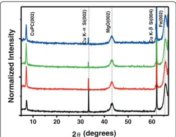
S7 Si(001)\8 nm MgO\15 nm Fe\1.8 nm MgO\1 nm CuPc23\60 nmα-NPD\70 nm Alq3\20 nm Al 10 20 30 40 50 60 Cu K-Si (004) Normalized Intensity 2 (degrees) Cu PC(002) MgO(002) Cu K-Si (002) F e (002)
Figure 2 X-ray diffractionθ-2θ scans with Cu Kα radiation for the 20-nm-thick CuPc films before and after thermal treatment.
damage to the underlying active organic emissive layer: CuPc as a hole-injection layer,N,N0-di(1-naphthyl)-N,N0 -diphenylbenzidine (α-NPD) as a hole-transport layer and 8-tris-hydroxyquinoline aluminum (Alq3) as a
light-emitting layer. During the deposition of the organic films, the pressure was kept no more than 2 × 10⁻⁶Torr, and the deposition rate was fixed at 0.03 nm/s. During deposition, the layer thickness was obtained by a quartz thickness monitor and verified after deposition by a step-profiler. The names of the TOLEDs with their structural information are listed in Table 1.
For the Si(001)/MgO/Fe/MgO/CuPc hybrid multilayers before and after vacuum annealing for 1 h in the temperature range from 100°C to 250°C, the structural characteristics were examined by using X-ray powder dif-fraction technique (XRD) and atomic force microscope (AFM). In order to analyze the microstructure of these hy-brid multilayer interfaces, cross-sectional samples for transmission electron microscope (TEM) were prepared using conventional mechanical polishing and dimpling techniques. All the images were obtained using a double aberration corrected JEOL FS2200 TEM (JEOL Ltd., Tokyo, Japan) with atomic resolution. A new specimen preparation process with minimum damage onto the or-ganic layer was developed. We used mechanical thinning, followed by precision ion-beam polisher system or (PIPS) with very short time to clean the surface. We have also minimized the damage during the TEM observation by re-ducing the e-beam exposure time. In addition we have
confirmed the presence of the CuPc by energy dispersive X-ray scan using the scanning TEM observation mode.
The current-voltage-luminance (I-V-L) characteristics were investigated by using a Keithley 236 source-measure unit and a Keithley 2000 multimeter equipped with a photomultiplier tube through an ARC 275 mono-chromator (Keithley Instruments Inc., Cleveland, OH, USA). The external quantum efficiency of the electro-luminescence (EL), defined as the ratio of the emitted photons to the injected electric charges, was calculated from the EL intensity measured by using a calibrated Si photodiode placed at a normal angle to the device’s surface.
Results and discussion
The main goal of this study was to obtain an enhance-ment of the thermal durability of the OLEDs. Particular attention was given to the engineering of charge inject-ing contacts by introducinject-ing the epitaxial thin MgO(001) layer. Figure 2 shows an important enhancement of ther-mal stability of the 20-nm-thick CuPc film grown the
(nm) (c) -2 0 2 0 250 500 750 1000 (n m ) (nm) 0 250 500 750 1000 1 µm X 1 µm (nm) 12 8 -8 -4 0 4 0 100 2 00 300 4 00 500 0 100 200 300 400 500 (n m ) (nm) (a) 500 nm X 500 nm 500 nm X 500 nm (b) (nm) 8 -4 0 4 0 100 200 300 400 500 0 100 200 300 400 (n m ) (nm) 500
Figure 3 AFM images of Si(001)/8 nm MgO/15 nm Fe/1.8 nm MgO/2 nm CuPc films. (a) as grown, post-annealed at (b) 150°C and (c) 250°C.
Table 2 RMS roughness for CuPc films after post-annealing for 1 h under vacuum
Post-annealing effect
HeatingT (°C) RMS (nm) Figure
0 (as grown film) 2.05 ± 0.40 Figure3a
150 1.79 ± 0.29 Figure3b 250 0.89 ± 0.05 Figure3c Si(001) substrate MgO(001) Fe(001) MgO(001) CuPc
Figure 4 Cross-sectional bright-field TEM image of Si(001)/8 nm MgO/15 nm Fe/1.8 nm MgO/20 nm CuPc film.
MgO(001) layer. Black color represents the result obtained before annealing, while red, green and blue col-ors correspond to the results for the sample after 1 h vacuum annealing at 250°C, 300°C and 350°C, respect-ively. The dashed lines represent CuPc, MgO and Fe peak positions from the powder diffraction file. After 1 h of vacuum annealing in the temperature range from 150°C to 350°C, a strong diffraction peak, corresponding to the (002) lattice plane of β-phase CuPc, persists at 2θ = 7.15° which is quite close to the position expected from the reference data. The peak intensity increases as the annealing temperature increases up to 250°C, while the intensity decreases after the annealing at 350°C. These XRD patterns indicate that the Fe and MgO buffer layers are strongly (001) textured, only the (002) diffraction peaks of bcc Fe and fcc MgO are observed. Consequently, the CuPc films deposited on the epitaxial Fe/MgO(001) buffer layer are also pre-dominantly (001) textured. Although several earlier works reported the occurrence of a phase transition
between α and β phases by thermal treatment above
200°C [15,16], but such a phase transition was not observed in this work.
Figure 3 shows the surface morphology of 20-nm-thick CuPc films (Figure 3a) before and after annealing at (Figure 3b) 150°C, and (Figure 3c) 250°C, respectively. Relatively smooth surfaces with root mean square (RMS) roughness of less than 2 nm were observed after the annealing up to 250°C. However, the RMS roughness be-came larger by annealing at the temperature higher than 250°C (Table 2). This is quite consistent with the strengthening of the [002] CuPc texture with increasing post-annealing temperature found by the XRD. This can simply reveal the enhancement of thermal stability and crystallinity of the CuPc layered structure due to the MgO(001) underlayer effect. From the AFM sur-face analysis, rather homogeneous roughness distribu-tions for the vertical distance between the highest peak and the lowest valley were observed in the range from −4 to 4 nm.
(b)
(a)
0 5 10 15 20 25 30 0.0 0.5 1.0 1.5Current Density (A/cm
2
)
Voltage(V)
Fe(001)\MgO(001) Fe(001) Poly Fe Al 0 5 10 15 20 25 30 0.0 0.2 0.4 0.6EL (a.u.)
Voltage (V)
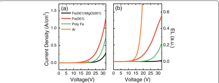
Figure 5 Current density-voltage and luminance-voltage characteristics for TOLED devices with different anodes. Al (blue, S1), Fe(100)/ MgO(100) (green, S2), Fe(100) (red, S3), and poly-Fe (black, S4) anodes. More detailed information about each sample structure is given in Table 1.
0 5 10 15 20 25 30 10-3 10-2 10-1 100 101 Current (mA) Voltage(V) 0 5 10 15 20 25 3010 -6 10-5 10-4 10-3 10-2 10-1 E.L. (a.u.) Voltage(V) (a) (b) 400 500 600 700 800 CuPc Thickness E.L.(arb.unit) Wave length(nm) 15 nm 5 nm 1 nm (c)
Here, we report a hybrid system consisting of a highly qualified interface between the MgO/Fe/MgO(001) and the OSC CuPc. Figure 4 corresponds to the TEM image for the 20-nm-thick CuPc film grown at RT. The image shows, from bottom to top, the Si substrate, the 8-nm-thick MgO buffer layer, and the 10-nm-8-nm-thick metallic Fe epilayer covered with the 1.8-nm-thick MgO. Note that the MgO/Fe/MgO(001) multilayers are well-crystallized, but some layer roughness is observable.
Figure 5 shows the current density-voltage (J-V) (Figure 5a) and the luminance-voltage (L-V) (Figure 5b) characteristics for the TOLED devices with 10-nm-thick CuPc film prepared beyond the different anodes, such as Al (blue, S1), polycrystalline Fe (poly-Fe) (black, S4), Fe (001) with (green, S2) and without MgO(001) (red, S3). For more details of the TOLED structure, see Table 1.
When compared to the TOLED devices based on Al and poly-Fe and Fe(001) bottom electrodes, the thresh-old voltage for the TOLED based on the Fe/MgO(001) electrode increases significantly. More drastic increase in the driving voltage is also shown for that Fe/MgO(001)-based TOLED. The large driving voltage could be attrib-uted to the larger work function of the MgO(001) layer (4.94 eV) [17] than that of Al (4.1 eV) [18] or poly-Fe (4.5 eV) [18]. Additionally, the effect of surface potential at the MgO(001)/CuPc interface could not be negligible. Since it was reported that charge injection barriers at metal/organic or oxide/organic interfaces affect the charge injection and recombination significantly [19-21],
we also investigated the I-V (Figure 6a) and L-V
(Figure 6b) characteristics for the Fe/MgO(001)-based TOLED with different CuPc thicknesses: 15 nm (red, S5), 5 nm (green, S6) and 1 nm (black, S7) as shown in Figure 6. The structure information of S5, 6 and 7 TOLED are given in Table 1. EL spectra of TOLED with different thickness of CuPc are shown in Figure 3c: red for S5, green for S6, and black for S7. When the thick-ness decreases from 15 to 1 nm, no remarkable change appeared in the threshold and driving voltages, but current and EL intensity increased obviously. A largely enhanced EL was observed in the TOLED with 1-nm-thick CuPc layer. To improve the TOLED device performance, further studies to optimize the device structure and fabrication conditions are required; the EL efficiency is far from perfect. However, our results sug-gest a new possibility to integrate spintronics with or-ganic electronics: The use of the epitaxial thin MgO (001) layer is proposed not only to improve the perform-ance and the stability of OLED, but also to inject the fully polarized spin current from the Fe/MgO(001) inter-face to the OSC layers [9]. Indeed, the enhanced thermal stability of a few-nanometer-thick CuPc films could re-sult from the MgO(001) underlayer effect: The (002)-textured β phase of CuPc layer persists even after the
vacuum annealing at 350°C. Significant work function al-teration by inserting MgO(001) between ferromagnetic metal and the CuPc OSC layer could provide a wide ver-satility of device functionality. For example, polarized light could be generated by fully polarized spin injection through the Fe/MgO(001) interface. Thus, for future work, it is worth to study the magnetic field effect in this OLED device.
Conclusions
In order to control the operation of an OLEDs, we investigated a new possibility of the use of thin MgO (001) layer between the ferromagnetic metal Fe(001)-OSC CuPc interface as a organic surface modifier. Re-markably enhanced thermal stability of CuPc films with smooth surface morphology (RMS roughness≤ approxi-mately 2 nm) was obtained up to the temperature of 350°C. In this work, the use of appropriate oxide layers could represent a new interface engineering technique for improving reliability and functionality in OSC devices. Based on the reliable Si(001)/MgO(001)/Fe (001)/MgO(001)/CuPc hybrid stack, the new TOLED structure was investigated for future organic spintronic device applications.
Competing interests
The authors declare that they have no competing interests.
Authors’ contributions
YJB and THK carried out the overall experiment and data analysis. NJL did the fabrication of OLEDs and the IVL experiments. HC and CL gave advice and helped for fabrication of OLEDs. LF and AH performed the TEM experiments. All authors read and approved the final manuscript.
Acknowledgements
This research is funded by the National Research Foundation of Korea (NRF) grants funded by the Ministry of Education, Science and Technology (MEST) (no. 2008-0062239, 2011-0017209, and 2010-0006749). YJB thanks the NRF (no. 2011-0001809) for the financial support.
Author details
1Department of Physics, Ewha Womans University, Seoul 120-750, South
Korea.2School of Electrical Engineering and Computer Science, Seoul
National University, Seoul 151-744, South Korea.3Department of Electronics,
The University of York, York YO10 5DD, UK.
Received: 1 October 2012 Accepted: 20 November 2012 Published: 26 November 2012
References
1. Campbell IH, Smith DI: Chapter 1. Physics of organic electronic devices. In Solid State Physics: Advances in Research and Applications. Vol. 55. San Diego: Academic Press; 2001:1–117.
2. Hamwi S, Meyer J, Kröger M, Winkler T, Witte M, Riedl T, Kahn A, Kowalsky W: The role of transition metal oxides in charge-generation layers for stacked organic light-emitting diodes. Adv Funct Mater 2010, 20:1762–1766.
3. Liao LS, Klubek KP, Tang CW: High-efficiency tandem organic light-emitting diodes. Appl Phys Lett 2004, 84:167–169.
4. Gao XD, Zhou J, Xie ZT, Ding BF, Qian YC, Ding XM, Hou XY: Mechanism of charge generation in p-type doped layer in the connection unit of tandem-type organic light-emitting devices. Appl Phys Lett 2008, 93:083304.
5. Matsumoto T, Nakada T, Endo J, Mori K, Kavamura N, Yokoi A, Kido J: Multiphoton organic EL device having charge generation layer. In Society for Information Display (SID) International Symposium: 2003 May 23; Baltimore. MD 2003, 34:979.
6. Qi X, Li N, Forrest SR: Analysis of metal-oxide-based charge generation layers used in stacked organic light-emitting diodes. J Appl Phys 2010, 107:014514.
7. Terai M, Fujita K, Tsutsui T: Capacitance measurement in organic thin-film device with internal charge separation zone. Jpn J Appl Phys 2005, 44:L1059–L1062.
8. Yuasa S, Nagahama T, Fukushima A, Suzuki Y, Ando K: Giant room-temperature magnetoresistance in single-crystal Fe/MgO/Fe magnetic tunnel junctions. Nat Mater 2004, 3:868–871.
9. Butler WH, Zhang X-G, Schulthess TC, MacLaren JM: Spin-dependent tunneling conductance of Fe|MgO|Fe sandwiches. Phys Rev B 2001, 63:054416.
10. Xiong ZH, Wu D, Vardeny ZV, Shi J: Giant magnetoresistance in organic spin-valves. Nature 2004, 427:821–824.
11. Barraud C, Seneor P, Mattana R, Fusil S, Bouzehouane K, Deranlot C, Graziosi P, Hueso L, Bergenti I, Dediu V, Petroff F, Fert A: Unravelling the role of the interface for spin injection into organic semiconductors. Nat Phys 2010, 6:615–620.
12. Campbell IH, Kress JD, Martin RL, Smith DL, Barashkov NN, Ferraris JP: Controlling charge injection in organic electronic devices using self-assembled monolayers. Applied Phys Lett 1997, 71:3528–3531. 13. Chapter 9. Molecular orbitals and electronic spectra of phthalocyanine
analogues. In Phthalocyanines: Properties and Applications, Volume 4. Edited by Snow JAW, Barger WR, Leznoff CC, Lever ABP. New York: Wiley; 1989. 14. Nakamuraa M, Tokumotob H: Molecular arrangement of copper
phthalocyanine on Si(001)-(2 × 1)-H: a high-resolution frictional force microscopy and molecular mechanics study. Surf Sci 1998, 398:143–153. 15. Barrett MA, Borkowska Z, Humphreys MW, Parsons R: Ellipsometry of thin
films of copper phthalocyanine. Thin Sol Films 1975, 28:289–302. 16. Kim EJ, Lim S, Lee E, Chab D, Friedmanc B: Effects of substrate
temperature on copper(II) phthalocyanine thin films. Appl Surf Sci 2003, 205:274–279.
17. Lim J, Oh J, Ko B, Cho J, Kang S, Cho G, Uhm H, Choi E: Work function of MgO single crystals from ion-induced secondary electron emission coefficient. J Appl Phys 2003, 94:764–769.
18. Haynes WM, Lide DR: Handbook of Chemistry and Physics. Boca Raton: CRC Press; 2011.
19. Castellani M, Salzmann I, Bugnon P, Yu S, Oehzelt M, Koch N: Structural and electronic implications for carrier injection into organic semiconductors. Appl Phys A 2009, 97:1–9.
20. Castellani M, Berner D: Competition between excitons and exciplexes: Experiments on multilayered organic light emitting diodes. J Appl Phys 2007, 102:024509.
21. Nüesch F, Si-Ahmed L, François B, Zuppiroli L: Derivatized electrodes in the construction of organic light emitting diodes. Adv Mater 1997, 9:222–225.
doi:10.1186/1556-276X-7-650
Cite this article as: Bae et al.: Growth and characterization of thin Cu-phthalocyanine films on MgO(001) layer for organic light-emitting diodes. Nanoscale Research Letters 2012 7:650.
Submit your manuscript to a
journal and benefi t from:
7 Convenient online submission 7 Rigorous peer review7 Immediate publication on acceptance 7 Open access: articles freely available online 7 High visibility within the fi eld
7 Retaining the copyright to your article