이용자는 아래의 조건을 따르는 경우에 한하여 자유롭게
l 이 저작물을 복제, 배포, 전송, 전시, 공연 및 방송할 수 있습니다. 다음과 같은 조건을 따라야 합니다:
l 귀하는, 이 저작물의 재이용이나 배포의 경우, 이 저작물에 적용된 이용허락조건 을 명확하게 나타내어야 합니다.
l 저작권자로부터 별도의 허가를 받으면 이러한 조건들은 적용되지 않습니다.
저작권법에 따른 이용자의 권리는 위의 내용에 의하여 영향을 받지 않습니다. 이것은 이용허락규약(Legal Code)을 이해하기 쉽게 요약한 것입니다.
Disclaimer
저작자표시. 귀하는 원저작자를 표시하여야 합니다.
비영리. 귀하는 이 저작물을 영리 목적으로 이용할 수 없습니다.
변경금지. 귀하는 이 저작물을 개작, 변형 또는 가공할 수 없습니다.
Design and Analysis of
All-Digital Phase-Locked Loop for Automotive CIS Interface
차량용 CIS Interface 를 위한
All-Digital Phase-Locked Loop 의 설계 및 분석
by
Heejin Yang
February, 2021
Department of Electrical and Computer Engineering College of Engineering
Seoul National University
All-Digital Phase-Locked Loop for Automotive CIS Interface
by
Heejin Yang
A Thesis Submitted to the Department of Electrical and Computer Engineering
in Partial Fulfillment of the Requirements for the Degree of Master of Science
at
SEOUL NATIONAL UNIVERSITY February, 2021
Committee in Charge:
Professor Sangwook Nam, Chairman
Professor Deog-Kyoon Jeong, Vice-Chairman
Professor Woo-Seok Choi
Abstract
Keywords : All-Digital Phase-Locked Loop (AD-PLL), Time-to-Digital Con- verter (TDC), Digitally Controlled Oscillator (DCO), Digital Loop Filter (DLF), Delta-Sigma Modulator (DSM), Phase Noise Analysis
Student Number : 2019-25170
This thesis presents design techniques for All-Digital Phase-Locked Loop (AD- PLL) assisting the automotive CMOS image sensor (CIS) interface. To target Gear 3 of the automotive physical system, the proposed AD-PLL has a wide operation range, low RMS jitter, and high PVT tolerance characteristics.
Detailed analysis of the loop dynamics and the noise analysis of AD-PLL are done by using Matlab and Verilog behavioral modeling simulation before an actual design. Based on that analysis, the optimal DLF gain configurations are yielded, and also, accurate output responses and performance are predictable. The design tech- niques to reduce the output RMS jitter are discussed thoroughly and utilized for actual implementation.
The proposed AD-PLL is fabricated in the 40 nm CMOS process and occupies an effective area of 0.026 mm2. The PLL output clock pulses exhibit an RMS jitter of 827 fs at 2 GHz. The power dissipation is 5.8 mW at 2 GHz, where the overall supply voltage domain is 0.9 V excluding the buffer which is 1.1 V domain.
Contents
ABSTRACT I
CONTENTS II
LIST OF FIGURES IV
LIST OF TABLES VII
CHAPTER 1 INTRODUCTION 1
1.1MOTIVATION ... 1
1.2THESIS ORGANIZATION ... 3
CHAPTER 2 BACKGROUND ON ALL-DIGITAL PLL 4 2.1OVERVIEW ... 4
2.2BUILDING BLOCKS OF AD-PLL ... 7
2.2.1TIME-TO-DIGITAL CONVERTER ... 7
2.2.2DIGITALLY-CONTROLLED OSCILLATOR ... 10
2.2.3DIGITAL LOOP FILTER ... 13
2.2.4DELTA-SIGMA MODULATOR ... 16
2.3PHASE NOISE ANALYSIS OF AD-PLL ... 20
2.3.1BASIC ASSUMPTION OF LINEAR ANALYSIS ... 20
2.3.2NOISE SOURCES OF AD-PLL ... 21
2.3.3EFFECTS OF LOOP DELAY ON AD-PLL ... 24
2.3.4PHASE NOISE ANALYSIS OF PROPOSED AD-PLL ... 26
CHAPTER 3 DESIGN OF ALL-DIGITAL PLL 28
3.1DESIGN CONSIDERATION ... 28
3.2OVERALL ARCHITECTURE ... 30
3.3CIRCUIT IMPLEMENTATION ... 32
3.3.1PFD-TDC ... 32
3.3.2DCO... 37
3.3.3DIGITAL BLOCK ... 43
3.3.4LEVEL SHIFTING BUFFER AND DIVIDER ... 45
CHAPTER 4 MEASUREMENT AND SIMULATION RESULTS 52 4.1DIE PHOTOMICROGRAPH ... 52
4.2MEASUREMENT SETUP ... 54
4.3TRANSIENT ANALYSIS ... 57
4.4PHASE NOISE AND SPUR PERFORMANCE ... 59
4.4.1FREE-RUNNING DCO ... 59
4.4.2PLLPERFORMANCE ... 61
4.5PERFORMANCE SUMMARY ... 65
CHAPTER 5 CONCLUSION 67
BIBLIOGRAPHY 68
초 록 72
List of Figures
FIG.2.1BLOCK DIAGRAM OF (A)CHARGE-PUMP PLL(B)ALL-DIGITAL PLL... 5
FIG.2.2TDCOPERATION ... 8
FIG.2.3TDCTRANSFER CURVE ... 8
FIG.2.4(A)DELAY LINE TDC(B)DIFFERENTIAL DELAY LINE TDC(C)VERNIER TDC ... 9
FIG.2.5TRANSFER CURVE OF DCO ... 11
FIG.2.6(A)CURRENT-CONTROLLED DCO(B)RESISTOR-CONTROLLED DCO ... 11
FIG.2.7(A)ANALOG LOOP FILTER (B)DIGITAL LOOP FILTER ... 13
FIG.2.8AN EXAMPLE OF DITHERING ... 17
FIG.2.91ST-ORDER DSMBLOCK DIAGRAM ... 18
FIG.2.10NOISE SHAPING FUNCTION OF THE 1ST AND 2ND-ORDER DSM ... 19
FIG.2.11OPERATION REGIONS OF A PLL ... 20
FIG.2.12NOISE SOURCES OF AD-PLL ... 21
FIG.2.13(A)BLOCK DIAGRAM OF AD-PLL WITHOUT LOOP DELAY (B) WITH LOOP DELAY . 25 FIG.2.14TOTAL PHASE NOISE PLOT OF AD-PLL ... 26
FIG.2.15CLOSED-LOOP GAIN TRANSFER FUNCTION OF AD-PLL ... 26
FIG.3.1OVERALL BLOCK DIAGRAM OF AD-PLL... 30
FIG.3.2PFD-TDCSTRUCTURE ... 32
FIG.3.3MONTE-CARLO SIMULATION RESULTS OF THE TDCRESOLUTION ... 33
FIG.3.4BB-PFDSTRUCTURE ... 34
FIG.3.5PFD-TDCGAIN CURVE ... 35
FIG.3.6THERMOMETER CODE SIMULATION ... 36
FIG.3.7BBUP /DOWN SIMULATION ... 36
FIG.3.8(A)PFDUP (DIVCLK=99MHZ)(B)PFDDOWN (DIVCLK=101MHZ) ... 37
FIG.3.9DCRSTRUCTURE IN DIAGRAM ... 38
FIG.3.10EVEN AND ODD CELL STRUCTURE IN DCR ... 39
FIG.3.11EQUIVALENT RESISTOR MODEL OF DCR ... 40
FIG.3.12DCOSTRUCTURE ... 41
FIG.3.13DCOFREQUENCY RANGE POST-LAYOUT SIMULATION RESULTS ... 42
FIG.3.14BLOCK DIAGRAM OF THE DIGITAL BLOCK ... 43
FIG.3.15DETAILED ARCHITECTURE OF THE DIGITAL BLOCK ... 44
FIG.3.16ACCOUPLED RESISTIVE FEEDBACK INVERTER STRUCTURE ... 47
FIG.3.17PHASE NOISE PLOT OF THE OUTPUT CLOCK PULSES (TT CORNER) ... 47
FIG.3.18OUTPUT CLOCK PULSES SKEW BASED ON THE POST SIMULATION RESULTS ... 48
FIG.3.19DIVIDER STRUCTURE ... 50
FIG.3.20(A)DIVIDE BY 2(B)DIVIDE BY 3(C)DIVIDE BY 5COUNTER ... 50
FIG.3.21OUTPUT CLOCK PULSES OF THE DIVIDER BASED ON THE POST-LAYOUT SIMULATION ... 51
FIG.4.1DIE PHOTOMICROGRAPH ... 53
FIG.4.2STRUCTURE OF TX OPEN-DRAIN DRIVER ... 55
FIG.4.3STRUCTURE OF RX CMLDRIVER ... 55
FIG.4.4MEASUREMENT ENVIRONMENT SET-UP ... 56
FIG.4.5FREQUENCY TRACKING BEHAVIOR AT (A)UP (B)DOWN CASE FINESIM ... 58
FIG.4.6MIN/TARGET/MAX FREE-RUNNING DCO CLOCK PULSES OF (A)TX (B)RX ... 59
FIG.4.7PHASE NOISE ANALYSIS OF 2GHZ FREE-RUNNING CLOCK PULSES ... 60
FIG.4.8SPECTRUM ANALYSIS OF 2GHZ FREE-RUNNING CLOCK PULSES ... 61
FIG.4.9(A)SPECTRUM ANALYSIS (B)PHASE NOISE ANALYSIS OF 2GHZ LOCKED CASE ... 61 FIG.4.10PHASE NOISE ANALYSIS WITH OPTIMAL GAIN (A)FINESIM (B)MATHEMATICAL
MODELING ... 62
FIG.4.11INTEGRATED RMSJITTER MEASURED BY 2DDLFGAIN SWEEP AUTOMATION CODE ... 64 FIG.4.12PHASE NOISE ANALYSIS AND SPECTRUM ANALYSIS WITH THE BEST DLFGAIN ... 64 FIG.4.13JITTER ANALYSIS WITH THE BEST DLFGAIN ... 64
List of Tables
TABLE 4.1PERFORMANCE COMPARISON ... 66
Chapter 1
Introduction
1.1 Motivation
Recently, automotive communication networks are rapidly evolving [1]. Especially for the Advanced Driver Assistance System (ADAS), a high-bandwidth transmission of high-resolution image data is crucial to utilize deep learning neural networks for complex computation. Therefore, the demand for high-resolution automotive CMOS image sensor (CIS) interface is increasing. However, there’s a lot of challenges be- cause of its harsh communication environment and the rigorous requirements on ro- bustness and reliability. Thus, to transfer reliable data with a multi-Gb/s transmission rate, accurate clock generation for both the transmitter and the receiver is the most essential.
All-Digital Phase-Locked Loop (AD-PLL) is emerging as a solution to combat this problem. Unlike Analog PLL, AD-PLL is beneficial in terms of its small area, high process-voltage-temperature (PVT) tolerance, scalability, programmability, and test- ability due to its digital nature. However, one of the challenges in designing AD-PLL is minimizing the quantization noise that occurs when converting analog values into digital values. In this work, based on the theoretical analysis, design techniques; such as designing a high-performance TDC, boosting the effective resolution of DCO, and noise shaping with DSM, to overcome such problems are addressed in depth. Moreo- ver, to satisfy the design specification of Gear 3 of the automotive physical system, whose main target data rate is 8 Gb/s with PAM-4 signaling, 8 phase 2 GHz Ring Oscillator is designed to support the half-rate signaling. Besides, to support Gear 1, 2, and to leave a margin for the possible extension toward Gear 4, the frequency range is set to be configurable from 1.5 GHz to 3 GHz. As a result, the proposed AD-PLL complies with every design requirement needed for the state of art CIS interface sys- tem and also achieves low output clock jitter. Note that the whole system is control- lable and adjustable digitally.
1.2 Thesis Organization
This thesis is organized as follows. Chapter 2 starts with the background of AD- PLL in terms of its structure and its loop dynamics. Then the operations of each build- ing block are explained and the effect of various noise sources on the output clock jitter is analyzed. Chapter 3 delves into the detailed circuit implementation of AD- PLL that has good phase noise characteristics. Specifically, it covers the design tech- niques to build high-resolution TDC, low jitter 4 Stage Ring Oscillator, and configu- rable DLF and DSM. Based on these design implementations in Chapter 3, Chapter 4 focuses on the post-layout simulation results and the analysis of the actual measure- ment results. Note that the automation code is utilized in the actual measurement pro- cess. The comparison table compares the performance of the proposed work with that of the other related state-of-the-art researches. Chapter 5 summarizes the proposed work and concludes this thesis.
Chapter 2
Background on All-Digital PLL
2.1 Overview
In the realm of high-speed link circuits, accurate data transmission and recovery is crucial. However, as the data rate increases, higher susceptibility to channel loss and inter-symbol-interference make low jitter clock generation and elaborate compensa- tion technique indispensable. Phase-Locked Loop (PLL) has been widely used in many circuits for a long time to generate clock pulses for this purpose.
PLL is a circuit that adjusts the phase and frequency of the internal clock by mini- mizing the phase and frequency error between the external clock and the internal clock through a feedback loop. Like any feedback system, PLL consists of three main com- ponents; a Producer that generates the output, a Sensor that measures the error
between the input and the output, and a Controller that adjusts the control of the pro- ducer based on the information given by the sensor. Depending on whether or not these main constituents are made digitally or could be handled with digital equivalents, PLL is classified into Digital PLL and Analog PLL.
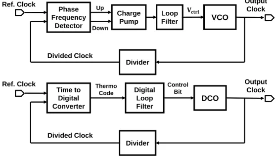
Fig. 2.1 Block Diagram of (a) Charge-Pump PLL (b) All-Digital PLL
Among various types of PLL in these two subgroups, Figure 2.1 shows the block diagram of the corresponding representatives; the Charge-Pump PLL (CP-PLL) and the All-Digital PLL (AD-PLL). Although CP-PLL has been extensively studied in the past few decades, the issues dealing with analog components such as leakage current, device mismatch, large area, and low voltage headroom are becoming more problem- atic as the CMOS technology scales down continuously. As a solution, AD-PLL, which is based on Digitally Controlled Oscillator (DCO) and Digital Loop Filter (DLF)
Phase Frequency
Detector
Loop
Filter VCO
Divider
Ref. Clock Output
Clock
Divided Clock Up
Down
Charge Pump
Control Time to Bit
Digital Converter
Digital Loop Filter
DCO
Divider Thermo
Code
Output Clock Ref. Clock
Divided Clock
instead of their analog counterparts, is proposed and has been investigated recently.
The key strengths of AD-PLL are in its high programmability, synthesizability, and PVT tolerance. In addition, since the building blocks are controlled with digital codes and there’s no need for analog tuning voltages, it is suitable for deep-submicron tech- nology with low supply voltage.
Despite these advantages, AD-PLL is prone to the quantization noise that occurs when converting analog values to digital values. Especially, the quantization noise of TDC and DCO is a critical factor in degrading the jitter performance. In the following sections, each of the building blocks will be explained in detail and the phase noise analysis to optimize overall jitter performance would be further addressed.
2.2 Building Blocks of AD-PLL
2.2.1 Time-to-Digital Converter
In AD-PLL, TDC converts the time difference between the reference clock and the divided clock into digital codewords. Figure 2.2 shows the basic operation of TDC.
When START rises, TDC starts to count the time difference Tin with the resolution
∆tTDC. This count continues until STOP changes from low to high. TDC’s output Dout can be expressed as Equation (2.1).
The transfer curve of TDC is shown in Figure 2.3. Unlike an analog PFD used in the CP-PLL, TDC performs an equal function but with a quantized output value. This results in quantization noise, which degrades the PLL jitter performance. The impact of TDC quantization noise in overall phase noise performance would be dealt with in the next section.
To reduce the effect of TDC quantization noise, TDC must have a high enough resolution. However, this would reduce the detection range, whose wideness is an- other important metric of designing TDC. Linearity, power, area are other require- ments that a TDC should satisfy.
Dout= Tout
∆tTDC =Tin− Terr,stop + Terr,start
∆tTDC (2.1)
Fig. 2.2 TDC Operation
Fig. 2.3 TDC Transfer Curve
TDC can be classified into a short time interval generation TDC which utilizes fine timing signal to translate time interval to digital code; a time stretching TDC which
Start
Stop
Reference
TDC input ( )
TDC output ()
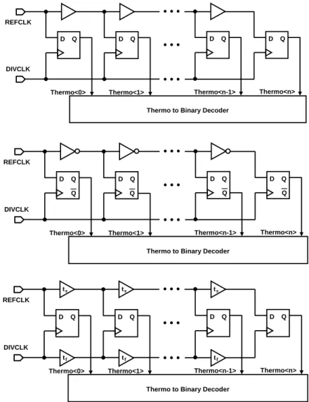
amplifies input time difference before feeding into the delay chain; and other un- grouped TDC, such as stochastic TDC [2], gated ring oscillator TDC [3]. Among these types, delay-line-based TDC, which belongs to the short time interval generation TDC, is the most widely used in digital PLLs.
Fig. 2.4 (a) Delay Line TDC (b) Differential Delay Line TDC (c) Vernier TDC
D Q D Q
…
…
…
D Q D Q
Thermo<0> Thermo<1> Thermo<n-1> Thermo<n>
REFCLK
DIVCLK
Thermo to Binary Decoder
D Q D Q
…
…
…
D Q D Q
Thermo<0> Thermo<1> Thermo<n-1> Thermo<n>
REFCLK
DIVCLK
Thermo to Binary Decoder ㅡQ
ㅡQ
ㅡQ
ㅡQ
D Q D Q
…
…
…
D Q D Q
Thermo<0> Thermo<1> Thermo<n-1> Thermo<n>
REFCLK
DIVCLK
Thermo to Binary Decoder
In Figure 2.4, three basic types of delay-line based TDC is shown. As readily seen, a simple delay line TDC in Figure 2.4 (a) has resolution with two inverter delay and a differential delay line TDC in Figure 2.4 (b) has resolution with one inverter delay by using differential D-Flip Flop. However, due to the device process limit, achieving high resolution is hard with these methods. To mitigate this problem, a Vernier delay line TDC in Figure 2.4 (c) is suggested. In this structure, the resolution is equal to the difference between ts and tf, which makes it possible to enhance TDC resolution to sub-gate-delay, even if the actual delay of each delay line is large [4].
2.2.2 Digitally-Controlled Oscillator
DCO generates an output clock with a frequency that is proportional to the input digital code. The transfer curve of DCO is shown in Figure 2.5. Whereas an analog Voltage-Controlled Oscillator (VCO) in the CP-PLL directly controls the frequency of an output clock with the input voltage, DCO controls the corresponding value with the Frequency Control Word (FCW). Therefore, the output value is discretized and the quantization noise occurs, which also degrades the PLL jitter performance.
To reduce such a malign effect, the frequency step size must be small, but at the same time fully covering the target frequency range in all PVT variation corners.
However, higher resolution and wider frequency range would increase the overall power consumption and area, so the designers have to compromise with this trade-off.
Fig. 2.5 Transfer curve of DCO
Fig. 2.6 (a) Current-Controlled DCO (b) Resistor-Controlled DCO
Since the phase noise and the power of DCO take up most of the corresponding values of the overall PLL system, meticulous efforts are needed in designing DCO. A typical way of implementing a DCO is to combine Digital-to-Analog Converter (DAC)
Frequency Control Word (FCW)
Frequency (Hz)
FCW
DAC
VCO
FCW
DAC
VCO
and analog VCO as shown in Figure 2.6. As in Figure 2.6 (a), a current-controlled DAC type controls the VCO output frequency by varying the current flowing through the VCO corresponding to the input digital code. Whereas in Figure 2.6 (b), a resistor- controlled DAC type controls the VCO output frequency by changing the resistance between the external supply voltage and the VCO supply voltage, thus changing the supply voltage of the VCO. Generally, a current-controlled DAC is better in terms of the phase noise performance but suffers more at the voltage headroom issue over a resistor-controlled DAC.
In addition, depending on the type of oscillator that DCO uses, DCO could be clas- sified into two groups; a Ring-DCO and an LC-DCO. The former benefits from its design simplicity to generate multi-phase output clock pulses, wider frequency tuning range, and its smaller occupancy in terms of area but it is poor at phase noise charac- teristics and is more sensitive to PVT variations than the latter. Based on these char- acteristics, the choice of an appropriate type of DCO is up to designers depending on one’s target application.
Besides, FCW could be implemented with a binary code or thermometer code. With N bits of code, in binary coding, the output frequency can have 2N values, whereas, in thermometer coding, only N values are obtainable. Despite this drawback in decod- ing hardware cost, since the thermometer code increases monotonically, utilizing the thermometer code can make the DAC safe from glitch problems. One way to utilize the advantages of the binary coding and the thermometer coding at the same time is to use a segmented thermometer scheme, which is the combination of the two. The
detailed implementation of DAC by using the segmented thermometer coding would be addressed in detail in the next chapter.
2.2.3 Digital Loop Filter
Loop Filter is a critical block that governs the loop dynamics of the overall system.
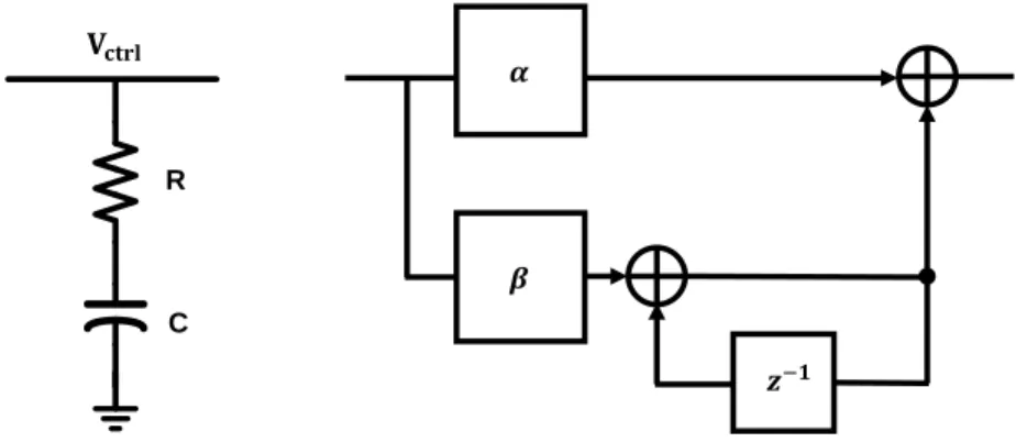
In CP-PLL, this is implemented with resistors and capacitors as shown in Figure 2.7 (a), which converts the charge pump current into the VCO control voltage Vctrl. As shown in Figure 2.7 (b), DLF in AD-PLL on the other hand, takes the TDC output as an input and generates a frequency control word for DCO, and this is all built digitally.
The digital nature of DLF brings many advantages. For example, since there is no capacitor in DLF, the system is free from leakage current issues. Also, a designer can adaptively configure gains of DLF to adjust the loop bandwidth of PLL without an additional cost of the area. Adaptive algorithms for fast locking or reducing jitter could be implemented also with ease. PVT tolerance is another merit of the DLF.
Fig. 2.7 (a) Analog Loop Filter (b) Digital Loop Filter R
C
q
A Loop Filter has both a proportional term and an integral term. Take an example of a first-order analog Loop Filter in Figure 2.7 (a). The transfer function can be rep- resented as Equation (2.2).
It can be inferred from this transfer function that the proportional term R tracks the transient phase error and the integral term 1
sC tracks the accumulating frequency error of the system. Another physical interpretation of these two terms in CP-PLL is that the capacitor sets the natural frequency 𝑤𝑛 and the resistor sets the damping factor ζ of the whole system. This could be derived from the closed-loop transfer function of CP-PLL, which can be expressed as following Equations (2.3) to (2.5). Note that the natural frequency has a significant effect on the CP-PLL loop bandwidth w3dB.
FLPF(s) =Vctrl(s)
ICP(s) = R + 1
sC (2.2)
HCP−PLL(s) =
IKVCO
2πC (RCs + 1) s2+IKVCOR
2πN s +IKVCO
2πCN
= N 2ζwns + wn2
s2+ 2ζwns + wn2 (2.3)
wn= √IKVCO
N2πC , ζ =R
2√ICKVCO
N2π =RC
2 wn (2.4)
w3dB= wn[2ζ2+ 1 + √(2ζ2+ 1)2+ 1 ]12 , PM = arctan (RC ∙ w3dB) (2.5)
Likewise, in a DLF in Figure 2.7 (b), an input signal in the proportional path is multiplied with the proportional gain 𝛼 and that in the integral path is multiplied with the integral gain 𝛽. These two paths perform the equivalent behavior with their ana- log counterparts, holding the phase and frequency information. The transfer function of DLF is given as Equation (2.6).
Since the z-domain representation of DLF is hard to interpret its physical meaning on the bandwidth and stability of AD-PLL, it is useful to use bilinear transform to convert the discrete-time z-domain system to the continuous-time s-domain system and vice versa. Bilinear transform in Equation (2.7) is derived from a first-order ap- proximation of the natural logarithm function that maps z-plane to s-plane.
Thus, with the help of bilinear transform, the corresponding transfer function of the analog Loop Filter in z-domain representation could be written down as Equation (2.8).
Besides, by equating Equation (2.5) and (2.7) the relationship between the digital gain 𝛼, 𝛽, and analog R, C could be derived as Equation (2.9). Note that the ratio of 𝛼 to 𝛽 in Equation (2.10) defines the phase margin and thus the stability of the AD-PLL system [5], [6].
FDLF(z) = α + β
1 − z−1 (2.6)
z = esT≈1 +sT 2 1 −sT
2
, s ≈2
T∙1 − z−1
1 + z−1 , T = DLF′s sampling period (2.7)
FLPF(z) = (R − T 2C) + (T
C) ∙ 1
1 − z−1 (2.8)
2.2.4 Delta-Sigma Modulator
A Delta-Sigma Modulator is an optional digital block in AD-PLL, however, it is a powerful tool for noise shaping and thus reducing the quantization noise of DCO. As mentioned before, the quantization noise is inversely proportional to the quantiza- tion resolution. Yet, due to the hardware limitation and the trade-off between the op- eration region and the resolution, there is a limitation in increasing the quantization resolution. As a solution, a dithering technique and a DSM emerged.
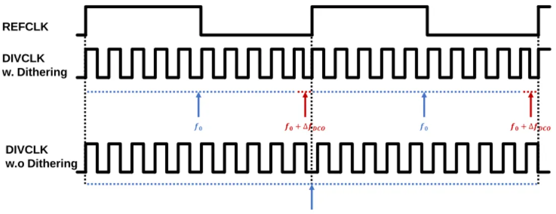
A dithering technique is a way of randomizing certain periodic sequences thus re- ducing undesired tones. By using the dithering technique in AD-PLL, it can effec- tively increase the resolution of the DCO. Consider a simple example of Figure 2.8.
Assume that PLL’s divide ratio is 10, and the frequency error between the reference clock and the divided clock is ∆𝑓𝐷𝐶𝑂. Without the dithering, the phase error would accumulate as time goes by. On the contrary, if the frequency of one cycle in DCO changes from 𝑓0 to 𝑓0+ ∆𝑓𝐷𝐶𝑂 in each reference clock, the phase error would go
α = R − T
2C , β =T
C (2.9)
α
β= tan (PM) T ∙ w3dB
−1
2 (2.10)
to zero. This makes the average frequency of DCO to 𝑓0+ ∆𝑓𝐷𝐶𝑂/10, which is equivalent to a tenfold increase in the quantization resolution of DCO. In general, if the DCO frequency is 𝑓0 in N cycles and 𝑓0+ ∆𝑓𝐷𝐶𝑂 in M cycles, the average fre- quency would be 𝑓0+ ∆𝑓𝐷𝐶𝑂∙M+NM , making the effective resolution M
M+N times.
However, one drawback is that it can generate spurs and inject dithering noises. By using a DSM, one can compensate for this.
Fig. 2.8 An Example of Dithering
The concept of rudimentary DSM is simple. Basically, it oversamples the signal until the sampling points are close enough to create correlated quantization errors between the consecutive samples, then subtracts the quantization error of one sample from the next to reduce the overall quantization noise. In Figure 2.9, a typical block diagram of DSM is shown. Written down in a mathematical formation, the relation- ship between the input x(t), the quantization noise q(t), and the output y(t) are given as Equation (2.11). By taking the z-transform of this, Equation (2.12) could be yielded.
REFCLK DIVCLK w. Dithering
DIVCLK w.o Dithering
In Equation (2.12), the output is the sum of two components; the input multiplied by z−1, and the quantization noise multiplied by 1 − z−1. The multiplier of the for- mer term is called a signal transfer function (STF) and the latter term is called a noise transfer function (NTF). Since the NTF (1 − z−1) exhibits a characteristic of a high pass filter, the spectrum of the quantization noise moves to a higher frequency.
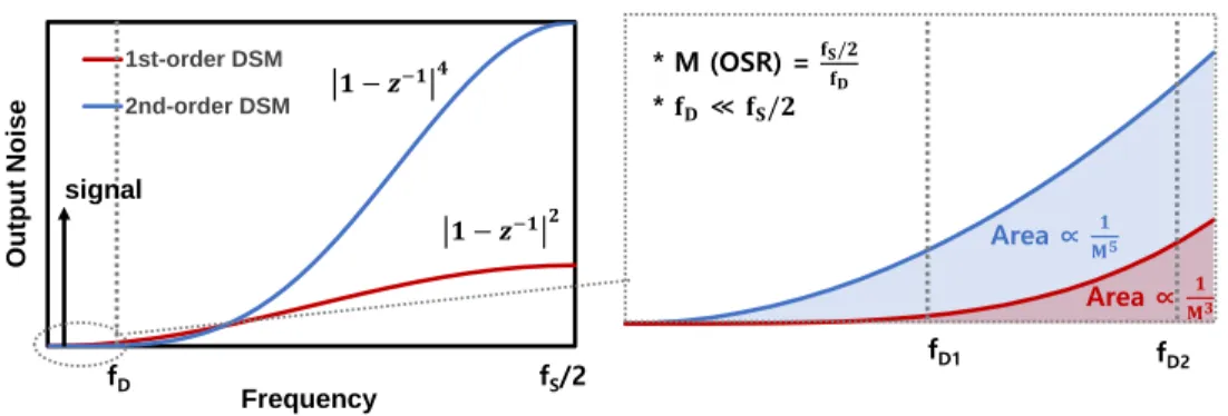
For higher M-th order DSMs, which are cascaded versions of the first order DSM, the NTF becomes (1 − z−1)M and they transfer more energy to the high-frequency region. An example of a noise shaping function is drawn in Figure 2.10. Note that the effect of reducing the quantization noise is proportional to both the order of DSM and the oversampling ratio (OSR), which is defined as fS/2
fD , where fD is an input signal’s bandwidth [7].
Fig. 2.9 1st-Order DSM Block Diagram
∫
DAC
x(t)+
-
ADC
y(t)q(t)
DELTA
SIGMA
𝑦(𝑘𝑇𝑠) = 𝑥((𝑘 − 1)𝑇𝑠) + 𝑞(𝑘𝑇𝑠) − 𝑞((𝑘 − 1)𝑇𝑠) (2.11)
𝑌(𝑧) = 𝑧−1𝑋(𝑧) + (1 − 𝑧−1)𝑄(𝑧) (2.12)
Fig. 2.10 Noise Shaping Function of the 1st and 2nd-Order DSM
1st-order DSM 2nd-order DSM
Frequency
Output Noise
fD fS/2
signal
fD1 fD2
Area ∝ Area ∝
* M (OSR) =
* ≪
2.3 Phase Noise Analysis of AD-PLL
2.3.1 Basic Assumption of Linear Analysis
PLL has four basic regions of operation which are the hold range, pull-in range, pull-out range, and lock range as depicted in Figure 2.11. Briefly explaining, the hold range denotes the frequency range that PLL can statically maintain phase track- ing, the pull-in range is the range that PLL will always become locked, the pull-out range is the range that PLL can dynamically sustain phase tracking, and finally, the lock range is the range that PLL locks within a single beat note between the refer- ence frequency and the output frequency [8].
Fig. 2.11 Operation Regions of a PLL
: Hold in range / static limits of stability : Pull in range
: Pull out range / dynamic limits of stability : Lock range
Among these regions, if PLL is in the lock range, the behavior of the PLL can be described with a linear model analysis. In other words, the basic assumption of the linear analysis is that the frequency error of the output signal to the reference signal is zero, and the phase error between the two is a constant value. Keeping in mind this basic assumption, let’s delve into the analysis of each noise source.
2.3.2 Noise Sources of AD-PLL
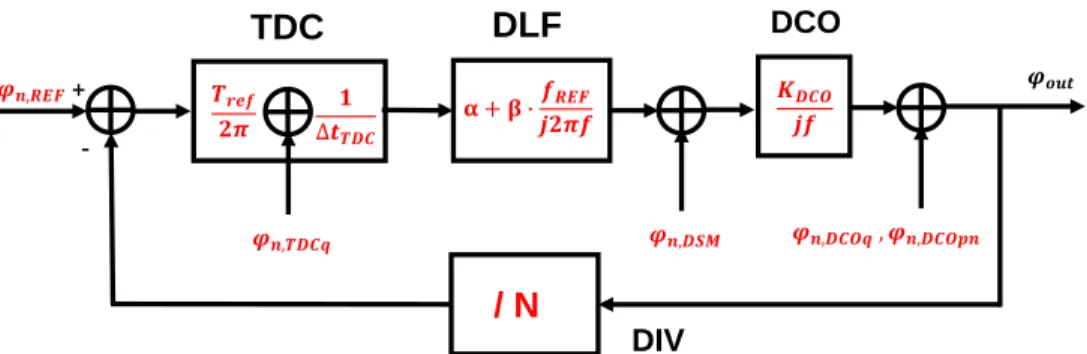
There are 5 internal noise sources in AD-PLL as shown in Figure 2.12; TDC Quantization Noise, DSM Dithering Noise, DCO Quantization Noise, DCO Phase Noise, and Reference Phase Noise. Each noise sources’ power spectral density (PSD) can be modeled as Equation (2.13) to (2.17). Note that the open-loop and the closed-loop transfer function is given as Equation (2.18) and (2.19) respectively.
Fig. 2.12 Noise Sources of AD-PLL
TDC DLF DCO
/ N
+ -
DIV
Then, by using the closed-loop gain of PLL, the output PSD of each noise source after passing the linear modeling of the PLL would be reduced to Equation (2.20) to (2.24). The total phase noise is equivalent to the sum of output phase noises of each noise source, as suggested in Equation (2.25). Besides, the RMS Jitter of the output clock could be calculated through Equation (2.26) [9], [10].
Sφn,TDCq(f) = (∆tTDC2 12fref
) ∙ (2π Tref
)
2
(2.13)
Sφn,DSM(f) = (∆fDCO,eff2 12f2fDSM
) ∙ (2sin( πf fDSM
))
2n
, n = order of DSM (2.14)
Sφn,DCOq(f) = (∆fDCO,eff2
12f2fref) ∙ (sinc( f fref))
2
(2.15)
Sφn,DCOpn(f) = (2FkT
PDCO) ∙ (1 + ( fDCO
2QDCOf)
2
) ∙ (1 +ff−3,DCO
f ) (2.16)
Sφn,REF(f) = (2FkT
PREF) ∙ (1 + ( fREF 2QDCOf)
2
) ∙ (1 +ff−3,REF
f ) (2.17)
Hop(f) = TrefKDCO
∆tTDC(j2πf)N∙ (α +βfref
j2πf) (2.18)
𝐺(f) = Hop(f)
1 + Hop(f)= Tref(j2πfα + βfref)KDCON
Tref(j2πfα + βfref)KDCO+ ∆tTDC(j2πf)2N= 1
𝑁∙ H𝑐𝑙(f)
(2.19)
In general, TDC quantization noise, DCO quantization noise, and DCO phase noise are the dominant sources of noise in AD-PLL. In addition, it can be inferred from the output phase noise equations that the TDC quantization noise is low pass filtered by the overall closed-loop gain function. However, the DCO quantization noise and DCO phase noise are high-pass filtered by this function. Thus, lower the loop bandwidth reduces the TDC quantization noise more but increases the other two more. Therefore, 𝑆𝜑𝑜𝑢𝑡,𝑇𝐷𝐶𝑞(𝑓) = 𝑆𝜑𝑛,𝑇𝐷𝐶𝑞(𝑓) ∙ |N ∙ G(f)|2 (2.20)
𝑆𝜑𝑜𝑢𝑡,𝐷𝑆𝑀(𝑓) = 𝑆𝜑𝑛,DSM(𝑓) ∙ |1 − G(f)|2 (2.21)
𝑆𝜑out,𝐷𝐶𝑂𝑞(𝑓) = 𝑆𝜑𝑛,DCO𝑞(𝑓) ∙ |1 − G(f)|2 (2.22)
𝑆𝜑out,𝐷𝐶𝑂𝑝𝑛(𝑓) = 𝑆𝜑𝑛,DCOpn(𝑓) ∙ |1 − G(f)|2 (2.23)
𝑆𝜑out,𝑅𝐸𝐹(𝑓) = 𝑆𝜑𝑛,REF(𝑓) ∙ |N ∙ G(f)|2 (2.24)
𝑆𝜑𝑜𝑢𝑡,total(𝑓) = 𝑆𝜑𝑜𝑢𝑡,𝑇𝐷𝐶𝑞(𝑓) + 𝑆𝜑𝑜𝑢𝑡,𝐷𝑆𝑀(𝑓) + 𝑆𝜑out,𝐷𝐶𝑂𝑞(𝑓)
+ 𝑆𝜑out,𝐷𝐶𝑂𝑝𝑛(𝑓) + 𝑆𝜑out,𝑅𝐸𝐹(𝑓) (2.25)
JRMS= 1 2πfc
∙ √2 ∫ 10L(f)10df
∞ 0
, L(f) =1
2∙ 𝑆𝜑𝑜𝑢𝑡,total(𝑓) (2.26)
adjusting α and β to an optimal value, considering the dominant noise sources is crucial in noise optimization of AD-PLL.
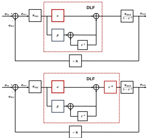
2.3.3 Effects of Loop Delay on AD-PLL
One of the nonidealities that one must consider in designing AD-PLL, is the effects of the loop delay. Because of the digital processing time in digital blocks, this loop delay occurs and changes the transfer function and the locking behavior. As shown in Figure 2.13, with the addition of z−D in the block diagram, the open-loop gain changes from Equation (2.27) to Equation (2.28). This adds additional zeros in the s- domain when converted with bilinear transformation, thus degrading the phase margin and stability.
Hopen,w.o,delay(z) = KTDC∙ (α + β ∙ 1
1 − z−1) ∙ KDCO
1 − z−1∙1
N (2.27)
Hopen,w,delay(z) = KTDC∙ (α + β ∙ 1
1 − z−1) ∙ z−D∙ KDCO 1 − z−1∙1
N (2.28)
Fig. 2.13 (a) Block Diagram of AD-PLL without Loop Delay (b) with Loop Delay
To minimize such malicious effects, one needs to make an effective loop delay smaller. Other than trying to reduce the number of clock edges that are required to update the information of TDC to DCO, making the digital domain clocking faster than the reference clock is one way of doing so. For example, if the total clock edge needed is twelve, and the digital clock is ten times faster than the reference clock, then the effective loop delay becomes 1.2 cycles, not 12 cycles. Besides, another method of reducing the effective loop delay is to make a direct bypass from TDC to DCO parallel to the original DLF path, enabling the faster update of information.
KTDC
+ -
− −
−
DLF
KTDC
+ -
− −
−
DLF
−
2.3.4 Phase Noise Analysis of Proposed AD-PLL
Fig. 2.14 Total Phase Noise Plot of AD-PLL (𝛂 = 𝟐−𝟓, 𝛃 = 𝟐− )
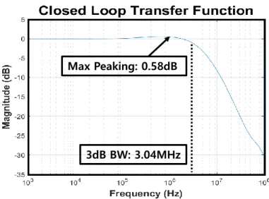
Fig. 2.15 Closed-Loop Gain Transfer Function of AD-PLL (𝛂 = 𝟐−𝟓, 𝛃 = 𝟐− ) Dominant Noise Source:
DCO Phase Noise
Max Peaking: 0.58dB
3dB BW: 3.04MHz
Based on the noise source analysis and considering the effect of loop delay and the techniques to alleviate its adverse effect dealt in the previous section, realistic phase noise analysis of the proposed AD-PLL is conducted. By using Matlab, the total phase noise plot could be drawn. Figure 2.14 shows the optimal total phase noise plot of AD-PLL based on the actual post-layout DCO phase noise and the delay modeling of implemented digital components. Specifically, -101 dBc/Hz DCO phase noise at 1 MHz offset, 100 MHz reference clock of phase noise -160 dBc/Hz, and divider factor of 20 is used. Besides, to reduce the effect of digital loop delay, the DLF frequency of 1 GHz, which is ten times faster than the reference frequency, is used. By sweeping the proportional gain and the integral gain of the loop filter, optimal values for jitter minimization are α = 2−5, β = 2−11 for this simulated model. The estimated RMS jitter integrated from 10 kHz to 40 MHz is 843 fs with 0.58 dB maximum peaking at 0.63 MHz, and the PLL loop bandwidth is 3.04 MHz with a phase margin of 68.9 . Note that the closed-loop transfer function of the system with this optimal gain con- figuration is depicted in Figure 2.15.
Chapter 3
Design of All-Digital PLL
3.1 Design Consideration
The AD-PLL proposed in this paper is designed to assist the automotive CIS inter- face system. The standard design specification is not firmly established yet, though, the overall requirements for this automotive physical system are discussed to be a maximum cable length of 10 m, and a channel bandwidth limit of about 2.5 GHz.
Besides, compared to the other applications, the automotive physical system empha- sizes more on the lower phase noise and higher robustness to PVT variations than lower power. This is because of the inherent characteristics of the automotive com- munication environment. Considering this and to support half-rate PAM-4 signaling of 8 Gb/s, which is the target downlink data rate of Gear 3, this paper suggests PVT tolerant, low phase noise 2 GHz AD-PLL.
Based on the phase noise analysis addressed before, PLL coefficients are set and the techniques introduced to make higher quantization resolutions are utilized for the design. For instance, the TDC resolution is set up to the physical limit to reduce the TDC quantization noise, and the digital blocks are synthesized with the highest fre- quency limit to improve the effective DCO resolution. Also, by using the first and the second-order DSM and the dithering technique, quantization noise shaping and boost- ing effective DCO resolution are possible. Furthermore, DCO is designed to cover the frequency range of 1.5 GHz to 3 GHz in every PVT corner and to generate 8-phase clock pulses with less skew to support phase interpolator-based half-rate clock and data recovery at the receiver.
3.2 Overall Architecture
The overall block diagram of the AD-PLL suggested in this paper is drawn in Fig- ure 3.1. The building blocks are PFD-TDC, DLF, DSM, DCO, AC-coupled buffer, and Divider, respectively. With the input of 100 MHz external clock pulses, the output clock pulses of 8 phases are generated by the overall AD-PLL system and sent to the transmitter and receiver.
Fig. 3.1 Overall Block Diagram of AD-PLL
Whereas a TDC can detect phase errors only, the PFD-TDC block can also track frequency error information by placing PFD parallel to the TDC. Comparing the edges of the reference clock and those of the divided clock, this block generates 7-bit output thermometer codes, which are fed into the digital block through clock domain con- version. Then, in the digital block, the information from the PFD-TDC is low-pass filtered by the DLF, generating a 25-bit code consisted of 10 integer bits and 15 frac- tional bits. These bits are sent to the DSM, which outputs 10-bit Frequency Control
DCO 100 MHz
Ref. Clock
8 phase Output Clock
Divided Clock
DSM 1st/2nd
Digital Block PFD
TDC
Buffer
DLF Clock
/ N
Z-1 / M
Word (FCW) that are decoded to 31-bit row code and 31-bit column code. These row and column codes control the Digitally Controlled Resistor (DCR) and the 4 stage Ring Oscillator generates the 8 phase output clock pulses with corresponding fre- quency. After passing AC coupled buffer to cover the full rail-to-rail swing of 1.1 V, the output clock pulses go to the other blocks of transmitter and receiver respectively.
Among these output clock pulses, two clock pulses with opposite phases are selected, and this pair operates the divider to generate the divided clock and the digital clock, perpetuating the feedback loop.
3.3 Circuit Implementation
3.3.1 PFD-TDC
As stated before, a TDC converts the time difference between the reference clock and the divided clock into digital codewords. However, the conventional TDC only operates as a Phase-Detector (PD), thus additional methods for frequency tracking are needed. The PFD-TDC used in this implementation of AD-PLL uses Bang-Bang Phase-Frequency-Detector (PFD) parallel to Vernier delay line TDC to perform both phase and frequency tracking [11]. The overall architecture is presented in Figure 3.2.
Fig. 3.2 PFD-TDC Structure
The resolution of the above PFD-TDC is equal to the difference between ts and tf, enhancing the TDC resolution to sub-gate-delay. To alleviate the burden of area, 7 delay cells and symmetric D-FF samplers [12] are used in total. Even and odd delay cells are separately implemented and REFCLK and REFCLKB are used for sampling
div<0>
D Q D Q
…
…
…
D Q D Q
Thermo<0> Thermo<1> Thermo<5> Thermo<6>
Divided Feedback Clock
Ref. Clock
ref<0> ref<1> ref<5> ref<6>
div<1> div<5> div<6>
respectively. Note that the use of the symmetric sampler is beneficial because the setup time for data ‘1’ and ‘0’ is equal to each other. For delay cell implementation, rather than using an inverter pair, an inverter is used. This lowers the possibility of code reversion resulting from the delay variations. The 7 delay cells yield the 7-bit thermometer code, thus the detection range of phase error is equivalent to 7(ts− tf).
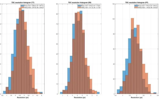
The sizing of the delay cell is determined by the Monte-Carlo simulation and the res- olution is set to 2.5 ps at TT corner (0.9V, 40), 1.9 ps at FF corner (1.0V, -40), 4.3 ps at SS corner (0.8V, 120). Corresponding simulation results are shown in Figure 3.3. Note that the reversion probability is 0.006 % (3.82σ) at even delay cell and 0.002 % (4.13σ) at odd delay cell at TT corner, thus satisfying the monotonicity.
Fig. 3.3 Monte-Carlo Simulation Results of the TDC Resolution
As in Figure 3.4, BB-PFD with the input of REFCLK<3> and DIVCLK<3> is placed in parallel with the TDC for frequency tracking purposes. The sampler operates at the positive edge of REFCLK<1>, holding its value until the next signal comes in.
If the phase difference of the inputs is in the TDC detection range, the PFD does not output UP, DN high signal, and for the other cases, the PFD produces UP or DN high signal according to the frequency relationship between the reference clock and the divided clock. Note that this dead zone control is done within the digital block and the total gain curve of PFD-TDC exhibits combined characteristics of PD and PFD as shown in Figure 3.5. Here, the proposed PFD-TDC has a PFD dead zone of 84 ps, and the TDC detection range of 17.5 ps.
Fig. 3.4 BB-PFD Structure
ref<3> div<3>
up dn
up
dn
BB_up
BB_dn
Fig. 3.5 PFD-TDC Gain Curve
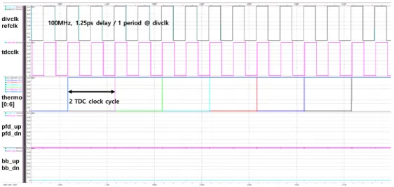
The simulation results of the PFD-TDC is shown in Figure 3.6, 3.7, and 3.8. In Figure 3.6, the 100 MHz reference clock and the 100 MHz divided clock with 1.25 ps phase delay per period are used for simulation, and the corresponding output ther- mometer code changed by 1 bit per twice the period. Also, as shown in Figure 3.7, by shifting the initial phase of the divided clock pulses by 0.1, the BB UP and DN high signals are generated respectively. Lastly, as presented in Figure 3.8, by using the 99 MHz and 101 MHz divided clock pulses, the PFD UP and DN high signals are produced properly. The total average power for the designed TDC is 0.51 mW.
-2π 2π
Phase Error (rad)
Digital Code
0 TTDC = 17.5 ps
TPFD = 84 ps
−7 0
PD PFD
7
TTDC= 2.5 ps
Fig. 3.6 Thermometer Code Simulation
Fig. 3.7 BB Up / Down Simulation
divclk refclk
tdcclk
thermo [0:6]
pfd_up pfd_dn
bb_up bb_dn
2 TDC clock cycle
100MHz, 1.25ps delay / 1 period @ divclk
refclk: 100MHz
divclk: 100MHz, -1ns delay (down) divclk: 100MHz, +1ns delay (up) BB_up for down case
BB_dn for down case BB_up for up case BB_dn for up case
Fig. 3.8 (a) PFD Up (DIVCLK = 99 MHz) (b) PFD Down (DIVCLK = 101 MHz)
3.3.2 DCO
The DCO in this proposed AD-PLL consists of a resistor-controlled DAC [13] and a pseudo-differential four-stage ring oscillator. The former is implemented with a 32
×32 current source array as shown in Figure 3.9. This Digitally-Controlled Resistor
refclk: 100MHz
divclk: 99MHz (up)
PFD_up for up case
PFD_dn for up case
refclk: 100MHz
divclk: 101MHz (down)
PFD_up for down case
PFD_dn for down case
(DCR), tunes the supply voltage of the subsequent ring oscillator by altering its re- sistance. This is done with a segmented thermometer scheme and glitch-reduction de- coding, which enables the serpentine switching as shown in the arrow in Figure 3.9.
It is noteworthy that only one switch is turned on and off at both column and row boundaries, thus minimizing the thermal switching noises at all possible codewords.
Another benefit of using suc