한국정보통신학회논문지(J. Korea Inst. Inf. Commun. Eng.) Vol. 20, No. 4 : 811~818 Apr. 2016
추가적인 부궤환 루프를 가지는 연속 미세 조절 위상 고정루프
최영식*
A Continuous Fine-Tuning Phase Locked Loop with Additional Negative Feedback Loop
Young-Shig Choi *
Department of Electronic Engineering, Pukyong National University, Busan 48513, Korea
요 약
추가적인 부궤환 루프를 가지는 연속 미세 조절 위상 고정루프를 소개하였다. 위상고정루프가 위상이 고정되지 않았을 때 위상고정루프는 연속적인 밴드 선택 루프를 통하여 빠르게 위상을 고정시키는 특성을 가지고 있다. 위상 고정루프가 고정 상태에 다다랐을 때 밴드 폭은 미세한 루프를 통해서 좁아진다. 추가적인 부궤환 루프는 안정성과 위상여유 성능을 향상시킨다. 0.18um CMOS 공정으로 제작한 위상고정루프의 결과 측정은 위상 잡음이 742.8MHz 캐리어 주파수로부터 2MHz 오프셋 주파수에서 –109.6dBc/Hz을 보여준다.
ABSTRACT
A continuous fine-tuning phase locked loop with an additional negative feedback loop has been proposed. When the phase locked loop is out-of-lock, the phase locked loop has a fast locking characteristic using the continuous band-selection loop. When the phase locked loop is near in-lock, the bandwidth is narrowed with the fine loop. The additional negative feedback loop consists of a voltage controlled oscillator, a frequency voltage converter and its internal loop filter. It serves a negative feedback function to the main phase locked loop, and improves the phase noise characteristics and the stability of the proposed phase locked loop. The additional negative feedback loop makes the continuous fine-tuning loop work stably without any voltage fluctuation in the loop filter. Measurement results of the fabricated phase locked loop in 0.18μm CMOS process show that the phase noise is -109.6dBc/Hz at 2MHz offset from 742.8MHz carrier frequency.
키워드 : 위상고정루프, 지속적인 밴드 선택, 두 가지 부궤환 루프, 위상 잡음
Key word : PLL, Continuous Band-selection, Two Negative Feedback Loops, Phase Noise
Received 07 January 2016, Revised 19 February 2016, Accepted 11 March 2016
* Corresponding Author Young-Shig Choi(E-mail:[email protected], Tel: +82-51-629-6222) Department of Electronic Engineering, Pukyong National University, Busan 48513, Korea
Open Access http://dx.doi.org/10.6109/jkiice.2016.20.4.811
print ISSN: 2234-4772 online ISSN: 2288-4165Ⅰ. INTRODUCTION
Phase-locked loops (PLLs) have been widely used to-date in many applications and it should have been expected that their performance would have been upgraded as in most other integrated chips. Typically, a PLL consists of a phase frequency detector (PFD), a charge pump (CP), a loop filter (LF), a voltage- controlled oscillator (VCO), and a divider [1]. A PLL is usually a third-order closed loop system that includes the second-order LF which consists of two capacitors and one resistor. It has one low frequency zero, and three poles consisting of two poles at origin and one pole at high frequency.
In general, a narrow bandwidth has an advantage for suppressing phase noise and spur, but it requires a low phase noise VCO and a long locking time. A higher frequency pole can be introduced to suppress phase noise further. Careful design of poles and zero location is required to ensure the stable operation of a PLL. The optimal loop-bandwidth has been derived from a discrete-time PLL model to find a loop-bandwidth which shows good jitter performance [2]. Jitter optimization using PLL design parameters has been derived [3]. These theories are helpful in the design of PLL, but their effect on fabricated PLLs is not great because they are susceptible to process variations.
There have been attempts to improve VCO performance with pre-distortion [4, 5] and feedback [6-10] methods.
The pre-distortion method does not produce the linear characteristic at low offset frequency range. The VCO with feedback loop demonstrates a noise reduction [6].
The VCO with feedback loop which is nested inside a PLL works as a robust linear characteristic VCO [7-9].
In [9], the role of the frequency voltage converter (FVC) is to provide a robust constant VCO gain insensitive to input voltage and temperature. The delay- discriminator- based feed-forward loop is used to cancel the phase noise of the VCO [10].
Integrated PLLs operate over a wide range of process and temperature variations, as well as a large range of
input and output conditions. Furthermore, the supply voltage of chips decreases as the process gets smaller.
For those reasons, PLLs need a large gain VCO which is the most important circuit in determining noise characteristics. PLLs with a large gain VCO degrade phase noise and reference spur performance. It is desirable to have a single widely-tunable PLL that still can provide fast locking and good phase noise characteristic. Usually in PLLs, the wide tuning range is realized with a fine tuning loop which selects one of several closely spaced multiple bands. Those bands cover a required wide tuning range. Various techniques have been published to find the correct band for a desired frequency [11-14]. The correct band is selected by measuring VCO frequency or monitoring VCO control voltage but locking time is long [11-14]. The period of the VCO and reference signals are converted to voltages which are compared to find the proper band with a little shorter locking time than the previous schemes [15]. A frequency–to-digital converter is used to find the correct band with the shortest locking time but a complicated digital circuit is required and results in a larger chip size [16].
In this paper, a continuous fine-tuning PLL with additional negative feedback loop is introduced to suppress phase noise with enhanced stability. The PLL has a PFD, a CP, a second-order LF, a VCO, a divider and a continuous fine-tuning circuit. The additional negative feedback loop consists of a VCO and a FVC. It serves a negative feedback function to the PLL loop, and improves the phase noise characteristics and the stability of the proposed PLL. The additional negative feedback loop makes the continuous fine-tuning loop work stably.
The rest of the paper is organized into five parts.
Section II discusses the theory of the proposed
continuous fine-tuning PLL with additional negative
feedback loop. Section III describes the noise analysis
of the proposed PLL. Section IV presents the circuits
used in the proposed PLL. Section V demonstrates
measurement and simulation results, and finally Section
VI provides some conclusions.
Ⅱ. PROPOSED CONTINUOUS FINE-TUNING PLL WITH ADDITIONAL NEGATIVE FEEDBACK LOOP
2.1. Continuous fine-tuning scheme
Fig. 1 (a) shows the proposed continuous fine-tuning PLL with additional negative feedback loop. It is made of a conventional PLL, locking status indicator (LSI), four switches (SW
1, SW
2, SW
3and SW
4), a continuous band-selection circuit and an additional negative feedback loop. Fig. 1 (b) shows the block diagram of the locking state indicator (LSI) and signal generator to generate Signal A, B, and C [17].
(a)
(b)
(c)
Fig. 1 (a) Continuous fine-tuning PLL with additional
negative feedback loop (b) Block diagram of locking state indicator (LSI) and signal generator (c) Timing diagrams of signal A, B, C.The PLL has a wide bandwidth at out of lock status to reduce locking time. The PLL has a narrow bandwidth at in-lock status to suppress phase noise.
When the PLL is out-of-lock, V
CON1is connected to the fixed voltage, V
BIAS, with the status of switches as in Table 1 and control signals as in Fig. 1 (c), respectively. The PLL is working on a coarse loop during the out-of-lock period. As the PLL approaches lock status, the status of the switches changes to near-in-lock as shown in Table 1. The output of the loop filter, V
LPF, is also connected to V
BIASfor a short time to make the voltages of V
CON1and V
LPFthe same.
The PLL is working on fine loop (lock status) after the short“on”time of signal A as the control signals changes as shown in Fig. 1(c). Additionally the negative feedback loop helps the PLL to work stably at out-of-lock status and near-in-lock status and suppress a little more phase noise at lock status.
The band selection circuit is made of comparators, switches, resistance and latches as shown in Fig. 2. When the PLL is out-of-lock, it is working on the band selection loop while the input of VCO, V
CON1, is connected to the fixed voltage, V
BIAS. V
COARSEis compared with the reference voltages from the resistance string. As V
COARSEvaries, “1” or “0” is generated at the comparators and stored at the latches.
Those “1” or “0” are used to select an appropriate fine VCO band. As the PLL approaches lock status, SW
2is
“off” and the coarse loop is disconnected from the loop filter. When the PLL is working on the coarse loop, it has a short locking time because of the wide bandwidth. This arrangement could be unstable due to its large VCO gain and optimized loop filter components for narrow bandwidth however the additional negative feedback loop ensures the PLL works like a conventional wide bandwidth PLL as explained in[18]. During lock status, the stored “1” or “0” at the latches is maintained to hold the selected fine VCO band. The PLL hence works as per a conventional narrow bandwidth PLL.
Fig. 3 shows the concept of the proposed continuous
fine-tuning scheme. When the output of the latches
varies, a band is selected while the input of the VCO on the fine loop is fixed. With the selected band, the PLL moves to lock status through near-in-lock status and works stably. The effective VCO gain when the PLL is out-of-lock is large as shown in Fig. 3.
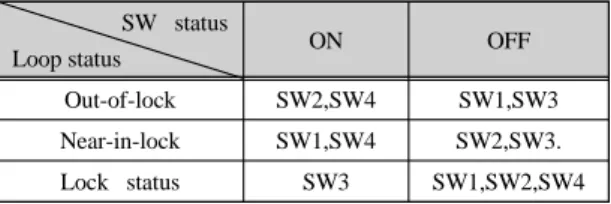
Table. 1 Status of switches according to PLL locking
statusSW status
Loop status ON OFF
Out-of-lock SW2,SW4 SW1,SW3
Near-in-lock SW1,SW4 SW2,SW3.
Lock status SW3 SW1,SW2,SW4
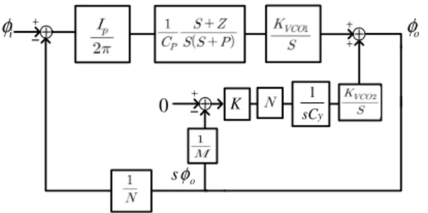
2.2. Function of additional negative feedback loop A PLL with an additional negative feedback loop is explained in [18]. When the output voltage of the loop filter changes, the output voltage of the additional negative feedback loop changes in the opposite direction at a much higher sampling frequency. Whenever the VCO output frequency varies, the additional negative feedback loop works as a compensator. It results instable operation when the PLL is working out-of-lock and a little more phase noise suppression by making the PLL work stably when the PLL is working at lock status. The linear model of the PLL with the additional negative feedback loop operating at fine loop is shown in Fig. 4. It consists of a PLL, in which the second-order LF is used, and the additional negative feedback loop which is made of an FVC and a VCO.
Fig. 2 Band selection circuit
Fig. 3 Correlation of V
CON1 and FOUT with band selection loop gain and fine loop VCO gainsThe FVC generates a voltage corresponding to the VCO output frequency at N/M times F
ref(N : Value of Divider’s division, M : Value of FVC’s input frequency division) and then the output voltage of the FVC controls the VCO output frequency as a negative feedback loop does. M is the division ratio of the divider in the FVC.
The closed and open loop transfer functions are as follows:
(1)
(2)
where, K is the FVC gain, K
VCO1and K
VCO2are the VCO gains, z is
and p is
. The open loop transfer always displays two zeros in the left half-plane because the term
∙
is always larger than the term
∙
in the numerator of the open loop transfer function
because K is much smaller than 1. The additional
negative feedback loop makes the PLL more stable.
+
⊕
−
φi +
⊕
+
2
KVCO
s
φo
+
⊕
−
0
s φ
oK
1sC
yFig. 4 A linear model of the PLL with an additional
negative feedback loopThe closed and open loop transfer functions of a conventional and the proposed PLL are plotted in Fig.
5. The magnitude of the closed loop transfer function of the PLL with additional negative feedback loop decreases at lower frequency and becomes equal to that of the conventional PLL at higher frequency which results in phase noise reduction as shown in Fig. 5.
Fig. 5 Closed transfer function of the PLL with additional
negative feedback loop PLL and conventional PLLⅢ. NOISE ANALYSIS
A linear model that contains all intrinsic noise sources is shown in Fig. 6. Z(s) is the loop filter transfer function as in Fig. 4. Each noise source is regarded as independent and its transfer function is expressed as follows.
Fig. 6 Linear model for noise analysis
(3)
(4)
(5)
(6)
(7)
K
LPFis LPF’s VCO gain K
FVCis FVC’s VCO gain.
Each of these equations contains the term
which comes from the additional negative feedback
loop. This term is efficacious in the respect of noise
suppression. In Fig. 7, all noise is suppressed in the
wide range of frequency by the FVC. If the gain of the
FVC is increased, the noise characteristics will be
further improved by this scheme.
(a)
(b)
Fig. 7 Noise Characteristic. (a) the conventional PLL,
(b) the PLL with an FVC. (Assuming similar noise magnitude)Ⅳ. CIRCUITS
The LSI and logic gates are used to generate control signals according to the operating status as shown in Table 1. The LSI generates “1” at near-in-lock status and “0” at out-of-lock status. With the output of the LSI, Signal A for SW
1, Signal B for SW
3and SW
4, Signal C for SW
2are generated to control switches as shown in Fig. 1(b).
The VCO has three inputs as shown in Fig. 8. Sixteen PMOSFETs are introduced per delay cell to select bands as BS
0-BS
7varies. The highest frequency is generated with all inputs of “0. A voltage controlled resistor (VCR) converts its input voltage variation into a large current variation, and then generates a wide range of VCO frequencies. The VCO is made of 3 differential
delay cells which have full output voltage swing and low output phase noise. The FVC used in the proposed PLL is shown in [18] and [19].
Fig. 8 A delay cell of the voltage controlled oscillator
Ⅴ. MEASUREMENT
The proposed continuous fine-tuning PLL with additional negative feedback loop is implemented in 0.18µm CMOS, and the chip photograph is shown in Fig. 9. The lower layers of transistors and capacitors are not seen because of the thick multi-inter-metal layers.
(a)
(b)
Fig. 9 (a) Chip photograph, and (b) layout of PLL with FVC
The die area is 680µm*480µm including the capacitor of the LF. Fig. 10 shows the measured phase noise of the proposed PLL with the FVC. The measured phase noise is -109dBc/Hz at 2MHz offset from the carrier frequency of 742.8MHz. The phase noise reduction of 10dB at 10KHz offset frequency occurs as expected as shown in Fig. 5.
Fig. 10 Measured phase noise
(a)
(b)
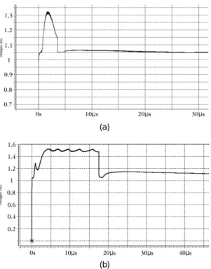
Fig. 11 Simulation results of V
LPF depending on the output of the band selection loop. BS0-BS7 : (a) 11110000 (b) 11000000Simulation is used to measure the locking time since there is no assigned pin for the loop filter output on the package. Fig, 11 shows that the locking process of the proposed PLL is similar to conventional PLL. Fig. 11 (a) and (b) show that the PLL is working on a coarse loop from power “on” to 3μs and 17μs. When the output of the band selection loop is 11000000, it shows the longest locking time of 17μs in simulation.
Ⅵ. CONCLUSION
An continuous fine-tuning PLL with additional negative feedback loop has been proposed. When the PLL is out-of-lock, it functions as per a conventional wide bandwidth PLL. When the PLL is in-lock, it functions as per a conventional narrow bandwidth PLL.
Addition of a negative feedback loop allows the PLL to function as per a conventional wide bandwidth PLL while also helping to suppress phase noise at the narrow bandwidth condition. Furthermore, the additional negative feedback loop helps the PLL to work stably at out-of lock status and near-in-lock status.
ACKNOWLEDGEMENTS
This work was supported by a Research Grant of Pukyong National University(2015)
REFERENCES
[ 1 ] Floyd M. Gardner, “Charge-Pump Phase-Lock Loop,”
IEEE J. Tran, on Communications, vol. COM-28, no. 11,
pp. 1849-1858, Nov. 1980.[ 2 ] K. Lim, C. Park, D. Kim and B. Kim, “A Low-Noise Phase-Locked Design by Loop Bandwidth Optimization,”
IEEE J. solid state circuits, vol. 35, no. 6, pp. 807-815,
June 2000.[ 3 ] Mozhgan Mansuri and Chih-Kong Ken Yang, “Jitter Optimization Based on Phase-Locked Loop Design Parameters,” IEEE J. solid state circuits, vol. 37, no. 11, pp. 1375-1382, Nov. 2002.
[ 4 ] J. Oehm and D. Pham-Stabner, “Linear Controlled Temperature Independent Varactor Circuitry,” in Proc.
28th Eur. Solid-State Circuits Conf., Sep. 2002, pp.
143-146.
[ 5 ] B. Hanafi and E. Hegazi, “A Technique for Truly linear LC VCO Tuning, a Proof of Concept,” in Proc. Int. Conf.
Microelectron., pp. 93-146, Dec. 2007.
[ 6 ] Y. Tokunaga, S. Sakiyama, A. Matsumoto and S. Dosho,
“An On-Chip CMOS Relaxation Oscillator with Voltage Averaging Feedback,” IEEE J. solid state circuits, vol. 45, no. 6, pp. 1150-1158, Jun. 2010.
[ 7 ] A. A. Abidi, “Linearization of Voltage-Controlled Oscillators using Switched Capacitor Feedback,” IEEE J.
solid state circuits, vol. 22, no. 3, pp. 494-496, Jun. 1987.
[ 8 ] M. Youssef, A. Zolfaghari, H. Darabi and A. A. Abidi, “A Low-Power Wideband Polar Transmitter for 3G Applications,”
in IEEE ISSCC Dig. Tech. Papers, pp. 378-380, 2011.
[ 9 ] M. Youssef, A. Zolfaghari, B. Mohammadi, H. Darabi and A. A. Abidi, “A Low-Power Wideband Polar Transmitter in 65-nm CMOS,” IEEE J. solid state circuits, vol. 46, no. 12, pp. 3061-3074, Dec. 2011.
[10] S. Min, T. Copani, S. Kiaei and B. Bakkaloglu, “A 90-nm CMOS 5-GHz Ring-Oscillator PLL with Delay-Discriminator- based Active Phase-Noise Cancellation,” IEEE J. solid state
circuits, vol. 48, no. 5, pp. 1151-1160, May 2013.
[11] W. B. Wilson, Un-Ku Moon, K. R. Lakshmikumar and L.
Dai, “A CMOS self-calibrating frequency synthesizer,”
IEEE J. Solid-State Circuits, vol.35, no.10, pp.1437-1444,
Oct. 2000.[12] H.I. Lee, J.K. Cho, K.S. Lee, I.C. Hwang, T.W. Ahn, K.S.
Nah and B.H. Park, “A ΔΣ fractional-N frequency synthesizer using a wide band integrated VCO and a fast AFC technique for GSM/GPRS/WCDM applications,”
IEEE J. Solid-State Circuits, vol.39, no.7, pp.1164-1169,
Jul. 2004[13] T. H. Lin and W. J. Kaiser, “A 900-MHz 2.5mA CMOS frequency synthesizer with an automatic SC tuning loop,”
IEEE J. Solid-State Circuits, vol.36, no.3, pp.424-431, Mar.
2001.
[14] Y.W. Chen, Y.H. Yu and Y.J. Emery Chen, “A 0.18-μm CMOS dual-band frequency synthesizer with spur reduction calibration,” IEEE Microwave and wireless components
letters, vol.23, no.10, pp. 551-553, Oct. 2013.
[15] T. H. Lin and Y. J. Lai, “Am agile VCO frequency calibration technique for a 10-GHz CMOS PLL,” IEEE J.
Solid-State Circuits, vol. 42, no.2, pp. 340-349, Feb. 2007.
[16] J. S. Shin and H. C. Shin, “A 1.9-3.8 GHz ΔΣ fractional-N PLL frequency synthesizer with fast auto-calibration of loop bandwidth and VCO frequency,” IEEE J. Solid-State
Circuits, vol.47, no.3, pp. 665-675, March. 2012.
[17] Y-G. Song, Y. S. Choi and J-G Ryu, “A phase-locked loop of the resistance and capacitance scaling scheme with multiple charge pump,” Analog Integr. Circ. Sig. Process, vol. 66, no. 2, 155-162, Feb. 2011.
[18] J. H. Nam, Y. S. Choi and M. G. Joo, “A single capacitor loop filter phase-locked loop with frequency voltage converter,” Analog Integr. Circ. Sig. Process, vol. 74, no. 1, pp. 193-201, Jan. 2013.
[19] Young-Shig Choi, “A Negative Feedback Looped Voltage-Controlled Ring Oscillator with Frequency Voltage Converter,” IEEE Trans. Microwave theory and techniques, vol. 61, no. 9, pp. 3271-3276, Sept. 2013.
최영식(Young-Shig Choi)
Received B.S. degree in Electronics Engineering from Kyungpook National University in 1982, M.S. degree from Texas A&M University in 1986 and Ph. D from Arizona State University in Electrical Engineering in 1993. From 1987 to 1999, he was with Hyundai Electronics (Now SK Hynix) as a principal circuit design engineer where he has been involved in the development of communication and mixed signal chips. From 1999 to 2003, he was with Dongeui University. In March 2003, he joined the faculty of Dept. of Electronics Engr. Pukyong National, where he is currently a Professor.
※관심분야 : PLL, DLL design