P1-9 / C.-S. Lin
• IMID 2009 DIGEST
Abstract
The negative bias temperature instability on LTPS TFTs in a darkened and an illuminated environment was investigated. Experimental results reveal that the generation of interface state density showed no change between the different NBTI stresses. The degradation of the grain boundary trap under illumination was more significant than for the darkened environment.
1. Introduction
Low-temperature polycrystalline-silicon thin- f i l m film transistors (LTPS TFTs) have been widely investigated for flat panel applications, such as for active matrix liquid crystal displays (AMLCDs)[1]. Compared to amorph ous silicon TFTs (a-Si TFTs), LTPS TFTs have higher electron mobility and driving current. Consequently, the LT PS TFTs can integrate both the pixel array and peripheral ci rcuits on the same glass substrate to realize a system-on-panel (SOP) display [2-3].Because driving circuits for LTPS TFTs are designed using the CMOS inverter structure , the reliability of the p-channel LTPS TFTs as understo- od by such measurements as negative bias temperature instability (NBTI) has been found to be an important proble m and has been widely investigated [4],[5],[6]. In addition, the LTPS TFTs are usually operated in illuminated environ ments on AMLCDs or SOP displays. Therefore, the NBTI u nder illumination is a very important issue for predicting LT PS TFTs degradation. The NBTI in p-channel LTPS TFTs under illumination of the degradation has not been adequate ly clarified.
2. Experimental
The p-channel LTPS TFTs were fabricated on a glass substrate with top-gate structures. First, a 500-nm-thick buffer-oxide was deposited on the glass. Next, a 50-nm a-Si film was deposited by plasma enhanced chemical vapor deposition (PECVD) on the buffer-oxide. Then, an a-Si-H film was crystallized by excimer laser annealing (ELA) at room temperature. An 80-nm gate oxide was deposited by PECVD and 300-nm Mo was deposited as a gate metal by sputtering. After the source and drain region formations, NH3 plasma treatment was utilized at 300 oC to passivate the dangling bonds at the poly-Si/SiO2 interface and at the grain boundaries. Finally, a 500-nm SiO2 layer was deposited and identified as the interlayer dielectric layer. The TFTs studied in this work are 6 μm in length and 10μm in width. During the stress operation, the device was stressed at a gate voltage of -25V with a grounded source/drain for 1000 sec under the darkened and the illuminated environments, at temperatures of 70 oC, 100 oC , 125 oC and 150 oC. The brightness of the front light used to provide photostatic stress was set at 400 lux. Reflected light also reaches the active layer via the Al thin film deposited atop the Si wafer that carries the device. During the measurement subsequent to the stress condition, all measurements were performed under darkened conditions with gate voltage swing from 5V to -10V and with the drain voltage set to -0.1V. The threshold voltage was determined as the gate voltage at which the drain current was equal to 9 nA in the sub-threshold region.
Illumination Assisted Negative Bias Temperature Instability
Degradation in Low-Temperature Polycrystalline Silicon Thin-Film
Transistors
Chia-Sheng Lin a, Ying-Chung Chen a, Ting-Chang Chang b, Wei-Che Hsu b, Shih-Ching Chen b, Hung-Wei Li c
a. Depart. of Electrical Engineering, National Sun Yat-Sen University, Kaohsiung, Taiwan, R. O. C Tel.: 886-7-5252000 ext. 3708, E-mail: [email protected]
b. Depart. of Physics, National Sun Yat-Sen University, Kaohsiung, Taiwan, R. O. C.
c .Depar . t of Photonics & Institute of Electro-Optical Engineering, National Chiao Tung University, Hsinchu, Taiwan, R. O. C
P1-9 / C.-S. Lin
IMID 2009 DIGEST •
3. Results and discussion
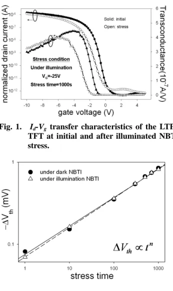
Figure 1 show the Id-Vg transfer characteristics for the
LTPS TFT after NBTI stress under illuminated conditions. It is clear from these figures that the subthreshold swing, the transconductance and the on-current have degraded for both the darkened and illuminated NBTI stress conditions. In addition, the Vth shifts to the negative direction under both NBTI stresses. In general, the threshold voltage (Vth)
shift of the TFT is caused by charge trapping or defect creation in the gate oxide. Such a Vth shift caused by
charge trapping requires a high electric field across the gate oxide (above 6 MV/cm). In this experiment, the electric field across the gate dielectric (about 3 MV/cm) is not high enough to cause hole injection. These experimental results are similar to previous studies for LTPS TFTs [4]. This indicates that interface states and grain boundary traps were generated during NBTI stress.
Figure 2 shows the negative shift of the threshold-voltage (-△Vth) with stress time under the darkened and illuminated NBTI stresses. The -△Vth increases with an increase in stress time, which displays power law dependence. The exponent factor n can be extracted by the power law relationship, △Vth=Atn[5], where n is 0.34 and 0.31 under the darkened and illuminated NBTI stresses, respectively. These results indicate the diffusion-controlled electrochemical reaction is the principal degradation mechanism for both the darkened and the illuminated NBTI stresses [8].
However, the differences between the darkened and il luminated NBTI stress is not readily apparent in Figs. 1 and 2. In order to better understand the influence of illuminatio n on NBTI stress, the generation of the interface state densit y (Nit) and the grain boundary traps (Ntrap) for both the stres
s conditions can be analyzed. In general, Nit can be extracte d from the subthreshold swing by neglecting the depletion c apacitance in the active layer according to the following eq uation [7].
⎟⎟
⎠
⎞
⎜⎜
⎝
⎛
⎥
⎦
⎤
⎢
⎣
⎡
−
⎟
⎠
⎞
⎜
⎝
⎛
⎟
⎠
⎞
⎜
⎝
⎛
=
q
C
kT
q
S
N
ox it1
10
ln
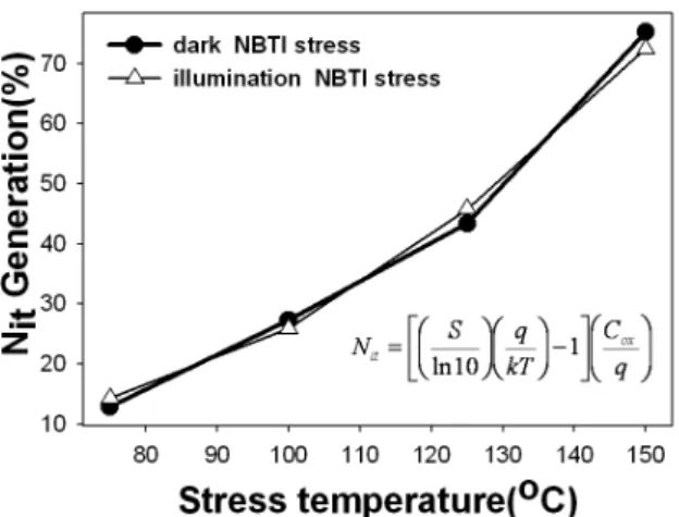
(1)In addition, the degradation and NBTI stress is strongly related to stress temperature. Therefore, both the darkened and illuminated stress temperatures were varied in a range from 75oC to 150oC. The correlation between the generation of the Nit and the stress temperature is illustrated in Fig. 3 (a). Clearly, the generation of the Nit after NBTI exhibits no difference between the darkened and illuminated environments, which suggests that the generation of the Nit is not strongly dependent on the extra hole generated under illumination. Figure 3 (b) shows the generation of the grain boundary trap states (Ntrap) at
various stress temperatures under both NBTI stresses; the Ntrap can be estimated by the Levinson and Proano method
[4],[6]. As can be seen in the figure, Ntrap generation under
illuminated NBTI stress is more pronounced than for the
darkened NBTI stress. This is due to the fact that more grain boundary trap states were created by the extra hole during illumination stress.
Figure 4 s h o w s t h e s c h e m a t i c d i a g r a m o f the device during the illuminated NBTI stress. Similar to th e darkened stress condition, there is formation of inversion holes between the poly-Si and the gate oxide— this is reflected in nearly identical values for Nit. However,
in addition to the inversion holes at the interface, light-induced electron-hole pairs are also generated in the poly-Si bulk- a fact reflected in the difference between Ntrap.
That is, degradation of the interface state is not sensitive to these extra holes from illumination. In poly-Si TFT, howe ver, there are many grain boundaries in the channel regions, and the passivated Si-H bonds in grain boundari es degrades under NBTI stress. During illuminated NB TI stress , the light induced holes will further react with the Si-H bonds in grain boundaries, causing more signi ficant Ntrap degradation. Moreover, the difference of
the Ntrap generation between the darkened and the illuminat
ed NBTI was more distinct at higher temperatures.
Fig. 1. Id-Vg transfer characteristics of the LTPS
TFT at initial and after illuminated NBTI stress.
Fig. 2 Relationship between negative threshold shift and stress time.
P1-9 / C.-S. Lin
• IMID 2009 DIGEST
Fig. 3 (a) Relationship between Nit generation at
different stress temperatures.
Fig. 3 (b) Relationship between Ntrap generation at
different stress temperatures.
Fig. 4. Schematic diagram of LTPS TFT cross section
and inversion charge and light-induced charge under illuminated NBTI stress.
4. Summary
In this work, the NBTI in p-type poly-silicon thin film transistors (poly-Si TFTs) under darkened and illuminated conditions was investigated. Degradation occurred on the threshold voltage, subthreshold swing and on-current in both NBTI stresses. For both darkened and illuminated stresses, the Nit degradation is similar due to the inversion holes and H dissociation at the interface. During illumination, however, the generation of extra holes in the poly-Si bulk causes the degradation of the Ntrap greater than
that during the darkened NBTI stress.
Acknowledgement
The work was supported by the National Science Council of Taiwan.
5. References
1. H. Kuriyama, S. Kiyama, S. Noguchi, T. Kuahara, S. Ishida, T. Nohda, K. Sano, H.Iwata, S. Tsuda, and S. Nakano, Tech. Dig. - Int. Electron Devices Meet., 563 (1991).
2. K. Yoneda, R. Yokoyama, and T. Yamada, Proc. Symp. VLSI Circuits, 85 (2001).
3. H. Tokioka, M. Agari, M. Inoue, T. Yamamoto, H. Murai, and H. Nagata, Proc. SID, 280 (2001).
4. C-Y Chen, J-W Lee, S-D Wang, M-S Shieh, P-H Lee, W-C W-Chen, H-Y Lin, K-L Yeh, and T-F Lei, IEEE Trans. Elec. Dev., 53, 2993 (2006).
5. A. T. Krishnan, V. Reddy, and S. Krishnan, IEDM Tech. Dig., 39.3.1 (2001).
6. E. Proano, R. S. Misage, and D. G. Ast, IEEE Trans. Elec. Dev. 36, 1915 (1989).
7 . C. A. Dimitriadis, P. A. Coxon, L. Dozsa, L. Papadimitriou, and N. Economou, IEEE Trans. Electron Devices, 39, 598 (1992).