A Spread Spectrum Clock Generator for SATA II with Rounded Hershey-Kiss Modulation Profile
Yong-Hwan Moon
*, Wan-Sik Lim
**, Tae-Ho Kim
*, Jin-Ku Kang
*★
Abstract
A spread spectrum clock generation is an efficient way to reduce electro-magnetic interference (EMI) radiation in modern mixed signal chip systems. The proposed circuit generates the spread spectrum clock by directly injecting the modulation voltage into the voltage-controlled oscillator (VCO) current source for SATA II. The resulting 33KHz modulation profile has a Hersey-Kiss shape with a rounded peak. The chip has been fabricated using 0.18㎛ CMOS process and test results show that the proposed circuit achieves 0.509% (5090ppm) down spreading at 1.5GHz and peak power reduction of 10㏈. The active chip area is 0.36㎜ × 0.49㎜ and the chip consumes 30㎽ power at 1.5GHz.
Key words: phase-locked loop (PLL), spread-spectrum clock generator (SSCG), modulation, EMI, serial-ATA (SATA)
* School of Electronics Engineering, Inha University
** LG Display Co. Ltd
★Corresponding author
※ Acknowledgment
This work is supported by Inha University and KIAT through the Human Resource Training Project for Strategic Technology. Authors also thank the IDEC program and for its hardware and software assistance for the design and simulation.
Manuscript received Jun. 3, 2011; revised Jun. 30, 2011
I. Introduction
The increasing speed of microprocessor, optical transmission links, intelligent hubs and routers is pushing the data rate into the gigabits-per-second range. As operating at high frequency, signals in the circuits and the printed circuit board (PCB) traces lead to great EMI. The EMI reduction of an electronics system is restricted to a certain level for a stable operation with other electronics systems.
The simplest way to reduce EMI is a shielding method: however, it cannot be applied to every system, especially to system-on-a-chip level. One of the most efficient ways to reduce EMI is spreading radiation energy out around the peak
frequency using a spread spectrum clock generator (SSCG). The data rate of SATA can go up to 3Gbps or 6Gbps. The spreading in SATA is 5000ppm down spreading with modulation frequency of 30~33KHz. A SSCG with PLL can either modulate the divider or the VCO control voltage directly. The direct modulation on the VCO is also investigated since added modulation profile is directly changing the frequency [1]-[4]. When modulating the divider, the modulation ratio depends on PLL bandwidth, so that it requires iterative design process to find optimum bandwidth. And the process, voltage, and temperature (PVT) variation could affect the modulation ratio. For small spreading ratio control, fractional-N type PLL with a sigma-delta modulator is often used [5]-[8].
In this paper, a SSCG with a rounded Hershey-Kiss modulation profile is presented for the application of SATA II. The proposed SSCG is modulating the gate voltage of the current source in the VCO delay cell. It brings a small deviation of VCO control voltage while the PLL is still locked.
The proposed SSCG is a simple approach and occupies smaller area compared to fractional-N PLL.
But still meets all SATA specifications.
II. Proposed SSCG
A. ArchitectureFig. 1 Block diagram of the proposed SSCG The proposed SSCG block diagram is shown in Fig. 1 with an integer type PLL and a modulation block. The modulation block is initiated by the reference frequency as a common input frequency.
Before PLL’s phase locking, the phase frequency detector (PFD) output in the PLL is a dominant component to pull the frequency up to the vicinity of 1.5GHz. The output of the modulation block is to spread VCO output frequency but does not disturb the main loop phase locking mechanism. After phase locking, small voltage variation to the current source in the VCO is injected by the modulation block. The injecting signal to the gate voltage of the current source in the VCO delay cell has a peak-to-peak value of 150 to 200㎷. This signal generate the fluctuation of the final VCO control voltage with PLL loop dynamics, which spreads the output frequency.
B. Modulation Block
The detailed modulation block is shown in Fig 2.
It composed of a 33KHz signal generator, level-shifter and a frequency modulation generator.
The 33KHz clock is generated by the 1st order sigma-delta modulator with a dual modulus divider.
Fig. 2 Modulation block
The reference clock is 150MHz. Since the dividing ratio is 4545.4545.., the summing integer value is 1000111000001(binary). Thus a 13 bit adder is needed. The fractional part is processed with 1st order sigma-delta modulator. Depending on the dividing ratio, a bit size of the adder can be adjusted. The modulation block occupies about 20%
of the total chip area.
The 33KHz square pulse is provided to the level shifter for the proper swing level. To make sure the VCO output frequency spreading, the bias level in the modulation circuit and its swing amplitude is to be set properly. The level-shifter produces the proper bias level and the signal amplitude. The level shifter circuit is derived from generating various voltage levels [9]. It has a single power supply and reduces a leakage current. The use capacitance in the circuit serves two purposes. It helps in preventing the quick discharge of node connected to the bottom plate and also acts as a startup when the circuit is powered up. The output of the level shifter is adjusted at around 1.05V. The operational amplifier (OP-amp) buffer protects the current path and modulates the VCO current source according to the output of the level shifter. The slew rate characteristic of the OP-amp converts the rectangular pulse of the level shifter output to triangular waveform. In order to generate the desired signal swing, the designed OP-amp has
±0.106㎷/㎲ slew rate.
Constant current biasing technique is used for keeping the slew rate constant across the PVT variations. The method aims at keeping the large signal characteristics intact across any temperature variation. However, since the g
mdrops with an increase in temperature, the op-amp needs to be designed to have enough bandwidth at a high temperature.
Fig. 3 shows a single stage of the ring type VCO circuit used in the proposed SSCG. The linearity of VCO gain is important to ensure the targeted spread ratio. To improve the linearity of the VCO the negative resistor circuit at the VCO output is added. The VCO gain is set at KVCO=2.2GHz/V.
Fig. 3 A single stage of the ring VCO
As shown Fig. 3, the M1 transistor is connected to a control voltage that was generated by the PLL.
The M8 transistor receives the modulation signal and this causes a controlled fluctuation of VCO frequency, which gives spectrum spreading.
C. Simulation Results
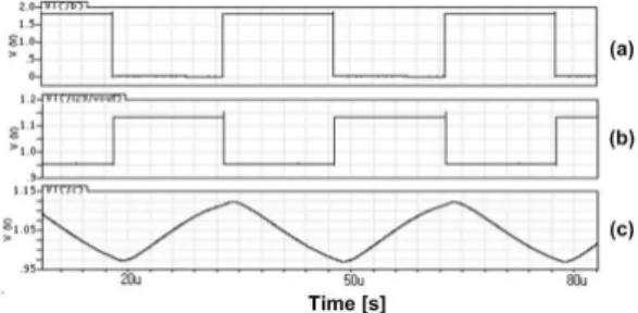
Fig. 4 shows the output signals at nodes in Fig. 2.
As shown in Fig. 4, the signal level and swing are shaped at nodes (a), (b), and (c) of Fig. 2. The modulation block produces 1.05V bias level and maintains modulation period. As shown in Fig. 4, the OP-amp output generates a triangle-like profile controlled by the slew-rate of the OP-amp. Since
Fig. 4 Simulated signals: (a) 33KHz clock generator (b) level shifter (C) OP-amp buffer output
Fig.5 Simulated modulation profile after locking
the output of the OP-amp is shaped by the RC time constant, the modulation signal is not the triangular shape. Therefore the modulation signal to the gate of VCO current source does not have linearity like a triangular profile. The slope of the modulation signal keeps changing as it goes up and down. And the rate of the slope variation is the maximum at the middle of signal swing. The slope variation of the modulation signal and the loop dynamics in the PLL make the final VCO control voltage be more like Hershey-Kiss Profile. The resistance in the filter attenuates the peak value of the control voltage and the capacitor in the filter causes a delay in the control voltage. Due to these loop filter characteristics the control voltage can not follow the fast slop changes. Thus the final shape of the control voltage becomes a rounded Hershey-Kiss Profile. The final modulation voltage is shown in Fig. 5. While generating the modulation profile, the PLL is locked.
III. Measurement Results
The proposed SSCG for SATA-II application was designed and implemented using CMOS N-well 0.18
㎛ 1-poly 6-metal process with 1.8V supply. Fig. 6 shows the chip microphotograph. Fig. 7 shows the PLL output spectrum of non-SSCG and SSCG mode. Comparing with the non-SSCG mode, the proposed SSCG circuit has the peak power reduction of 10.2㏈, which meets the SATA specification (>7
㏈). Also it shows down spread ratio of 0.509%
(5090ppm).
Fig. 6 Chip microphotograph of the proposed SSCG
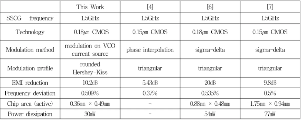
This Work [4] [6] [7]
SSCG frequency 1.5GHz 1.5GHz 1.5GHz 1.5GHz
Technology 0.18㎛ CMOS 0.15㎛ CMOS 0.18㎛ CMOS 0.15㎛ CMOS
Modulation method modulation on VCO
current source phase interpolation sigma-delta sigma-delta Modulation profile rounded
Hershey-Kiss triangular triangular triangular
EMI reduction 10.2㏈ 5.43㏈ 20㏈ 9.8㏈
Frequency deviation 0.509% 0.37% 0.535% 0.5%
Chip area (active) 0.36㎜ × 0.49㎜ - 0.88㎜ × 0.48㎜ 1.75㎜ × 0.94㎜
Power dissipation 30㎽ - 54㎽ 77㎽
Table 1: Proposed SSCG performance summary (a)
(b)
Fig. 7 Measured spectra with (a) non-SSCG mode and (b) the proposed SSCG mode at 1.5 GHz
The chip occupies chip area of 0.36㎜ × 0.49㎜ and consumes 30㎽ at 1.5GHz. Table 1 gives the performance summary of the proposed circuit and
comparisons with previous works. The proposed SSCG shows the minimum chip area and lowest power consumption compared to other schemes while demonstrating a reasonable EMI peak power reduction (~10㏈).
IV. Conclusion
The proposed architecture generates a spread spectrum clock by directly injecting the modulation into the VCO current source for SATA II application. The modulation frequency is set at 33 KHz and the modulation profile is controlled by OP-amp slew-rate. The final VCO control voltage profile is a Hersey-Kiss shape with a rounded peak.
The chip has been fabricated using 0.18㎛ CMOS process and test results show 0.509% (5090ppm) down spreading at 1.5GHz and peak power reduction of 10.2㏈. The proposed SSCG shows the smaller chip area and lower power consumption while demonstrating a reasonable EMI peak power reduction (~10㏈).
References
[1] Wei-Ta chen, Jen-Chien Hsu, "A Spread Spectrum Clock Generator for SATA-II," IEEE ISCAS, vol. 3, pp. 2643-2646, May 2005.
[2] Chao-Chyun Chen, et. al., "A Spread Spectrum Clock Generator Using a Capacitor Multiplication Technique," Emerging Information Technology Conference, Aug. 2005.
Wan-Sik Lim (Member)
2006 : BS degree in Electronics Engineering, Inha University.
2008 : MS degree in Electronics Engineering, Inha University.
2008 ~ : LG Display
Tae-Ho Kim (Student member) 2007 : BS degree in Electronics Engineering, Inha University.
2009 : MS degree in Electronics Engineering, Inha University.
2009 ~ : PhD candidate in Electronics Engineering, Inha University.
Jin-Ku Kang (Member)
1996 : PhD degree in Electrical and Computer Engineering, north Carolina State University.
1983~1988 : Research Engineer, Samsung Electronics.
1996~1997 : Senior Design Engineer, Intel(U.S).
1997 ~ Present : Professor, Inha University [3] Hsiang Hui Chang, "A Spread Spectrum Clock
Generator With Triangular Modulation," IEEE JSSC, vol. 38, no. 4, pp. 673-676, Apr. 2003.
[4] M. Aoyama et al., "3 Gb/s, 5000ppm Spread Spectrum SerDes PHY with Frequency Tracking Phase Interpolator for Serial ATA," IEEE Symp.
VLSI Circuits, pp. 107-110, Jun. 2003.
[5] Deok-Soo Kim, Deog-Kyoon Jeong, "A Spread Spectrum Clock Generation PLL with Dual tone Modulation Profile," IEEE Symp. VLSI Circuits, pp.
96-99, Jun. 2005.
[6] Masaru Kokubo et al., "Spread-Spectrum Clock Generator for Serial ATA using Fractional PLL Controlled by ΔΣ Modulator with Level Shifter", IEEE ISSCC, vol. 1, pp. 162-163, Feb. 2005.
[7] Hyung-Rok Lee, et al., "A Low-Jitter 5000ppm Spread Spectrum Clock Generator for Multi-channel SATA Transceiver in 0.18μm CMOS," IEEE ISSCC, vol. 1, pp. 160-161, Feb. 2005.
[8] Ching-Yuan Yang, et al., "A 3.2GHz Down- Spread Spectrum Clock Generator using a Nested Fractional Topology," IEICE Trans. Fundamentals, vol. E91-A, no. 2, pp. 497-503, Feb. 2008.
[9] Quadeer A. Khan, et al., "A Single Supply Level Shifter for Multi Voltage System," VLSI Design, Jan.
2006.
BIOGRAPHY
Yong-Hwan Moon (Student member) 2002 : BS degree in Electronics Engineering, Inha University.
2004 : MS degree in Electronics Engineering, Inha University.
2004 ~ Ph.D candidate in Electronics Engineering, Inha University