42
논문번호 08-03-07
(172)
An Improved Triangular/Square-Wave VCO Using OTAs
Jin-Woong Jeong
*, Chang-Su Won
*, Won-Sup Chung
*★
Abstract
An improved triangular/square-wave VCO using OTAs is presented. It consists of two OTAs, a timing capacitor, and a resistor. A prototype circuit built with commercially available components exhibits less than 0.01% nonlinearity in its current-to-frequency transfer characteristic from 0.2 to 14 kHz and 450 ppm/°C temperature coefficient of frequency over -20°C to 40°C.
Key words: Triangular/square-wave generator, Voltage-controlled oscillator(VCO), Current-controlled oscillator, Schmitt trigger, Operational transconductance amplifier(OTA),
Ⅰ. Introduction
Triangular/square-wave voltage-controlled oscilla- tors (VCOs) have a wide range of applications in instrumentation and communication systems. Such VCOs with wide sweep capability can easily be realized by using an operational transconductance amplifier (OTA) as a switching current source to charge and discharge a grounded timing capacitor followed by a Schmitt trigger [1]-[3]. These realizations require a high-performance voltage comparator to form a Schmitt trigger and hence the resulting VCOs become complex and e·pensive. In this paper, a new scheme is presented where the Schmitt trigger is implemented with another OTA
* School of Electronics and information Engineering, Cheongju University
★professor of Electronics and information Engineering e-Mail : [email protected], Tel : 043-229-8462
※ Acknowledgment
The authors are grateful to Chang-Hyeon Lee of the Department of Semiconductor Engineering, Cheongju University, for SPICE simulation and breadboard experiment.
Manuscript received Feb. 17, 2008 ; revised Aug. 25, 2008
instead of the conventional voltage comparator.
Since the OTA exhibits the simpler configuration than the voltage comparator, the proposed VCO features a simple configuration. It, however, retains the wide sweep capability and good linearity of voltage to frequency.
Fig. 1. Circuit diagram of the proposed VCO.
An Improved Triangular/Square-Wave VCO Using OTAs 43
(173) t
t0 t1 t2
vC
2
IB
C
2
IB
−C
1
RIB
−
1
RIB
(a)
t
T1 T2
T
1
RIB
1
RIB
− vR
(b)
Fig. 2. Output waveforms of the VCO.
II. Circuit Description
The proposed VCO is shown in Fig. 1. OTA1 and the resistor
R
form a current-controllable Schmitt trigger whose threshold voltage is proportional to the bias currentI
B1. OTA2 and the timing capacitorC
from an integrator whose time constant is proportional to the bias currentI
B2. The waveforms associated with the circuit is shown in Fig. 2.To see how the VCO operates, let the output of the Schmitt trigger be at its positive saturation level of L+ = RIB1. A current equal to
I
B2 will flow through the capacitorC
, causing the output of the integrator to linearly increase with a slope ofI
B2/ C
. This will continue until the integrator reaches the high thresholdV
TH= RI
B1 of the Schmitt trigger, at which point the schmitt trigger will switch states, its output becoming negative and equal toL
-= -RI
B1.
At this moment the current throughC
will reverse its direction. It follows that the integrator output will start to decrease linearly with a negative slope of equal to -I
B2/ C
. This will continue until the integrator output voltage reaches the low threshold voltage of the Schmitt trigger,V
TL= -RI
B1. At this point the Schmitt trigger switches,its output becomes positive (
L
+= RI
B1), the current throughC
reverses direction, and the output of integrator starts to increase linearly, beginning a new cycle.From the above description it is easy to derive an expression for the period of the square and triangular waveforms. During the interval
T
1 we have, from Fig. 2(a),
(1)
from which we obtain
(2)
Similarly, during
T
2 we have
(3)
from which we obtain
(4)
Equations (2) and (4) can be combined to obtain the period
T
of the output waves as
(5)
from which we obtain the oscillation frequency given by
(6)
Ⅲ. Experimental Results
The VCO shown in Fig. 1 was built with LM13600 OTAs and a polystyrene capacitor of 1 nF. The resistor used was
R
= 100 ㏀ and its tolerance is 0.5%. A simple current mirror and a resistor were used for producing a current source.The bias current
I
B1 was set to 10 ㎂ for convenience and all measurement were performed at supply voltages of ±5 V. The oscillation frequency against bias currentI
B2 was measured over the bias current range of 1
50 ㎂. For comparison, the conventional VCO in [3] was also investigated. The results are plotted in Fig. 3. It appears that the linearity error of the proposed VCO is less than 0.01 % while that of the conventional VCO is less than 0.02 %. The nonlinearity is mainly caused by the switching delay of the OTA2. The linearity44 전기전자학회 논문지(Journal of IKEEE) Vol. 12. No.3
(174) improvement of the proposed VCO is achieved by connecting the inverting input terminal of OTA2 to its output terminal, thereby the net input voltage of OTA2 at switching moments becomes about two time larger than the conventional case. The larger
Bias current IB2[㎂ ]
0 10 20 30 40 50 60
Oscillation frequency[kHz]
0 2 4 6 8 10 12 14 16
Linearty error(%)
-0.10 -0.08 -0.06 -0.04 -0.02 0.00 0.02 0.04 0.06 0.08 0.10
Conventional circuit New circuit Conventional circuit New circuit
Fig. 3. Measured oscillation frequency against bias current
I
B2.Bias current IB2 [㎂ ]
0 10 20 30 40 50 60
Temperature stability [PPM/]℃
100 200 300 400 500 600 700
Conventional circuit New circuit
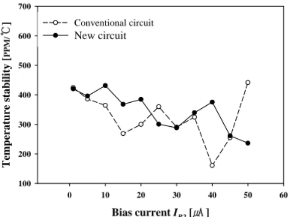
Fig. 4. Measured temperature stability against temperature.
the input voltage of OTA2 becomes, the faster OTA2 saturates. This results in reducing the switching delay of OTA2. Fig. 4 shows the temperature stability of the output frequency measured over a temperature range from -20 °C to 40 °C. The temperature stability is maintained to within 450 ppm/°C over the frequency range of 0.2-14 kHz. Fig. 5 shows the oscillation frequency changes due to the power-supply voltage changes when
I
B2 = 10 ㎂. It indicates that the proposedVCO is less sensitive than the conventional one to the power-supply changes.
Bias voltage VCC, VEE [V]
2.5 3.0 3.5 4.0 4.5 5.0 5.5
Oscillation frequency [kHz]
2.76 2.77 2.78 2.79 2.80 2.81
Conventional circuit New circuit
Fig. 5. Oscillation frequency changes due to the supply-supply voltage changes when
I
B2 = 10 ㎂.Ⅳ. Conclusion
An improved triangular/square-wave VCO using OTAs has been described. It features a simple configuration. An additional feature is the linear and wide controllability of frequency by a dc current.
because of these properties the proposed VCO is expected to find wide applications in communication and instrumentation systems.
References
[1] J. W. Haslett, “Current-switching linear VCO."
Electron
.Lett.
, vol. 25, pp. 139-140, Jan. 1989.[2] W.-S. Chung, H.-W. Cha and K.-H. Kim,
“Temperature-stable VCO based on operational transconductance amplifiers,"
Electron. lett.
, vol. 26, pp. 1900-1901, Oct. 1990.[3]
National Operational Amplifiers Databook
,: pp.1-631-1-648, National Semiconductor Corp, Santa Clara CA 1995.
n Improved Triangular/Square-Wave VCO Using OTAs 45
(175)
BIOGRAPHY
Jeong Jin-Woong
2007 : BS degree in Semicon- ductor design Engineering, Cheongju University
2007. 3~: He is Studing a MS degree in Electronic Engineer- ing, Cheongju University
Won Chang-Soo
2005 : BS degree in Informa- tion communication Engineering, Cheongju University
2007 : MS degree in Electrical Engineering, Cheongju University 2008. 3~ : He is Studing a PhD degree in Semiconductor Engi- neering, Cheongju University
Chung Won-Sup (Member)
1997 : BS degree in Electrical communication Engineering, Hanyang University
1979 : MS degree in Electrical communication Engineering, Hanyang University
1986 : PhD degree in
Electrical science Engineering, Shizuoka University
1986. 4. ~ : professor in the Department of Semiconductor engineering , Cheongju University