1. Introduction
CuInGaSe
2(CIGS) based thin film solar cells have achieved high efficiency with the absorber of very thin thickness because it’s a direct bandgap semiconductor and have high optical absorption coefficient. In the last few years the CIGS solar cell efficiencies of about 20% have been recorded, which makes it an useful material to replace silicon solar cells; therefore, the CIGS thin film is one of the most promising solar cell absorber layer material to be used in the next generation photovoltaic researches
1). The reduction of the production cost and the development of reproducible large scale manufacturing modules are key factors for the employment of CIGS solar cells in the photovoltaic field. CIGS thin films have been prepared using a variety of techniques including co-evaporation, sputtering, electrochemical deposition and chemical spray pyrolysis
1-8). Co-evaporation process which has achieved the highest efficiency by NREL is the most successful technique for the preparation of CIGS thin films. However, this method makes mass production
and scale up of large area devices extremely difficult because of its complicate processing steps using Cu, In, Ga and Se elements
3). On the other hand, the sputtering process typically provides fast deposition rate, excellent reproducibility, and good morphology for obtaining high-quality, large-area CIGS thin films. Also sputtering process has the advantage of stoichiometry transfer of the target material to substrate film. The properties of CIGS thin films are very sensitive to deposition conditions hence the deposition conditions of sputtering technique employed to prepare CIGS thin films are of particular importance
3).
The properties of the CIGS films have a strong relationship with the stoichiometry of the films. In order to obtain high conversion efficiency, the film should have a suitable stoichiometry of Cu, In, Ga and Se elements in the film. Due to the low vapor pressure of elemental Se, post selenization was required in order to obtain the desired CIGS stoichiometry. Recently, the fabrication techniques of quaternary target containing Cu, In, Ga and Se have been improved so that CIGS thin films can be deposited by sputtering process without post selenization
4).
The structural, optical and electrical properties of sputter- deposited CIGS thin films were directly influenced by the sputtering process parameters such as substrate temperature, working pressure, RF power and distance between target and
Effect of KCN Treatment on Cu-Se Secondary Phase of One-step Sputter-deposited CIGS Thin Films Using Quaternary Target
Sung Hee Jung ․ Ji Hyun Choi ․ Chee Won Chung*
Department of Chemical Engineering, Inha University 100 Inharo, Nam-gu, Incheon 402-751, Korea
ABSTRACT: The structural, optical and electrical properties of sputter-deposited CIGS films were directly influenced by the sputtering process parameters such as substrate temperature, working pressure, RF power and distance between target and substrate. CIGS thin films deposited by using a quaternary target revealed to be Se deficient due to Se low vapor pressure. This Se deficiency affected the overall stoichiometry of the films, causing the films to be Cu-rich. Current tends to pass through the Cu-Se channels which act as the shunting path increasing the film conductivity. The crystal structure of CIGS thin films depends on the substrate orientation due to the influence of surface morphology, grain size and stress of Mo substrate. The excess of Cu was removed from the CIGS films by KCN treatment, achieving a suitable Cu concentration (referred as Cu-poor) for the fabrication of solar cell. Due to high Cu concentrations on the CIGS film surface induced by Cu-Se phases after CIGS film deposition, KCN treatment proved to be necessary for the fabrication of high efficiency solar cells. Also during KCN treatment, dislocation density and lattice parameter decreased as excess Cu was removed, resulting in increase of bandgap and the decrease of conductivity of CIGS films. It was revealed that Cu-Se secondary phase could be removed by KCN wet etching of CIGS films, allowing the fabrication of high efficiency absorber layer.
Key words: Cu(In
1-xGa
x)Se
2, absorber layer, thin film solar cell, RF sputtering, KCN etching
*Corresponding author: [email protected] Received June 18, 2014; Revised July 15, 2014;
Accepted July 15, 2014
ⓒ 2014 by Korea Photovoltaic Society
This is an Open Access article distributed under the terms of the Creative Commons Attribution Non-Commercial License (http://creativecommons.org/licenses/by-nc/3.0)
which permits unrestricted non-commercial use, distribution, and reproduction in any medium, provided the original work is properly cited.
88
substrate
9,10). According to previous researches, the RF power and distance between target and substrate have the effect on the improvement of deposition rate while the properties of CIGS thin films show little change. Up to date, several researches have reported that substrate temperature and working pressure have a strong influence on the properties of the film
3,11,12). CIGS thin films deposited by using a quaternary target revealed to be Se deficient due to Se low vapor pressure. This Se deficiency affected the overall stoichiometry of the films, causing the films to be Cu-rich. Previous studies reported negative effects on the cell efficiency due to the presence of Cu-Se channels in Cu-rich CIGS thin films. Current tends to pass through the Cu-Se channels which act as the shunting path, resulting in increasing the film conductivity
11,13). The crystal structure of CIGS thin films depends on the substrate orientation due to the influence of surface morphology, grain size and stress of Mo substrate
14). Therefore, we suspect that the crystal structure of CIGS thin films deposited on glass and Mo substrates can be different.
In this study CIGS thin films were deposited on Mo substrate by RF sputtering of quaternary CIGS target, followed by KCN treatment in order to obtain Cu-poor films. The electrical and optical properties of both Cu-rich and Cu-poor films were compared.
2. Experimental Details
CIGS thin films were prepared on Mo coated soda lime glass by a one-step RF magnetron sputtering system. Mo thin films were deposited as an electrode by DC sputtering on a soda lime glass of 1 μm thickness. A 3 in. diameter quaternary target composed of Cu, In, Ga and Se elements with atomic percent ratios of 25, 17.5, 7.5, 50, respectively was employed. The deposition chamber was evacuated to a base pressure of 0.93-1.20 x 10
-4Pa using a turbomolecular pump backed up by a mechanical pump. Sputtering process was carried out with an Ar flow rate of 30sccm. An RF power of 80 W was applied to the CIGS target. The distance between target and substrate was fixed at 6.0 cm and the substrate was rotated at the speed of 10 rpm. During deposition, the substrate temperature was held at 400°C and the chamber pressure was varied from 0.13 Pa to 2.0 Pa. The overall thickness of all CIGS thin films were around 1 μm.
Prior to the film deposition, pre-sputtering was carried out for 15 min to remove any contaminants from the target surface.
The thickness of CIGS films was measured by using a Tencor-P1 surface profiler. Philips X’Pert PRO X-ray diffraction (XRD) analysis using Cu K
αirradiation was employed to examine the crystalline structure of the films. Microstructure and surface morphology of the films were observed using HITACHI S-4300 field emission scanning electron microscopy (FESEM). Energy dispersive x-ray spectroscopy (EDX) with a beam energy of 15 keV was used to investigate the element contents of the films. The bandgap of CIGS films were evaluated from the measurements of optical transmittance through the films using Lambda spectroscopy from 400 nm to 2500 nm. The carrier concentration and resistivity of CIGS films were measured using Van der Pauw method through HMS-3000 Hall effect measurement system in 0.55 T magnetic fields at room temperature.
In soldering in Hall effect measurement was applied onto the surface as the ohmic contact.
3. Results and Discussion
CIGS thin films of 1 μm thickness were deposited using a single quaternary target by RF magnetron sputtering on Mo coated soda lime glass. An RF power of 80 W was employed, substrate temperature was maintained at 400°C in order to crystallize the films during deposition, and working pressure was varied from 0.13 Pa to 2.0 Pa. Wet etching by KCN solution (hereafter called KCN treatment) was carried out in order to remove Cu-Se secondary phase from the surface of CIGS films.
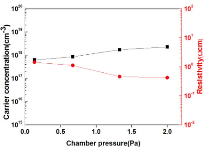
Fig. 1 shows the carrier concentration and resistivity of the CIGS films deposited under various working pressures, which were obtained by Hall effect measurement. When working
Fig. 1. Carrier concentration and resistivity of CIGS thin films deposited at various working pressures from 0.13 Pa to 2.0 Pa
pressure increased, the carrier concentration increased and resistivity decreased from 10
0to 10
-1Ωcm. The decrease in the film resistivity is attributed to the formation of metallic impurities on the film, presumably Cu-Se secondary phases.
The chalcopyrite phase of the CIGS films should possess high resistivity (10
0~10
1Ωcm) in order to achieve a high efficiency CIGS solar cell.
The XRD patterns of the CIGS films deposited under different working pressures are shown in Fig. 2. All films presented several peaks near 26.9°, 44.65° and 52.94° locations corresponding to (112), (220), and (312) crystal planes, which reveal the existence of the CIGS chalcopyrite structure (JCPDS 35-1102). The peak locations of XRD corresponding to the chalcopyrite structure are in good agreement with those of CuIn
0.7Ga
0.3Se
2films. As the working pressure increase from 0.13 Pa to 2 Pa, the intensity of (112) peak decreased, revealing that at high working pressures, the collisions between Ar ions and sputtered ions reduce the deposition rate and uniform incident onto the substrate due to the scattering event, therefore reducing the film crystallinity
15,16).
CIGS films exhibit a dominant diffraction peak at (112) plane, due to the movement of sputtered particles to lower energy sites, in order to achieve higher stability on the substrate surface. According to phase diagram of CIGS materials, CIGS films tend to have mixed chalcopyrite CIGS and Cu
2-xSe phases
17). However, the diffraction peaks of Cu
2-xSe phases could not be detected because they are close enough to overlap with CIGS peaks. Therefore, we can deduce that the value of R
I(112) is close to 1 hence the films exhibits strong texture for
(112) orientation for all working pressures, suggesting that the films are Cu-rich. R
I(112) was defined as the ratio of the (112) diffraction peak intensity to the sum of all the peaks intensities in the XRD patterns
18):
(1)
Where I(hkl) is the intensity of (hkl) peak.
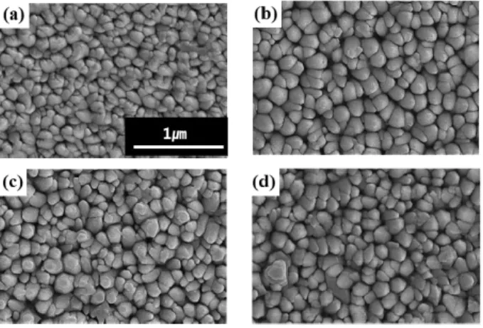
Fig. 3 shows the surface morphologies of as-deposited CIGS thin films at various working pressures. All of the CIGS films have polycrystalline phases with densely packed grains. The variation in working pressure strongly affected the film density.
As the working pressure increases; the mean free path of the CIGS atoms is reduced by collisions between sputtered CIGS particles and Ar ions
10). Atomic collisions increase the possibility of low mobility particles to be deposited on the substrate surface;
therefore decreasing the CIGS film density and yielding uniform and well grown grains of 200 nm in diameter. However at high working pressures of 2 Pa, the SEM micrographs revealed that the particles were decreased to be irregular shape. We assume that the small particles are less-grown impurities, mostly composed of Cu-Se secondary phases. The Cu-Se secondary phase can be removed by treating the films in a KCN solution.
The surface morphology of KCN treated as-deposited CIGS films is shown in Fig. 4. SEM micrographs revealed that by wet etching the CIGS films with a KCN solution, impurities were removed, resulting in clear and uniform CIGS films. The particles size did not change but the surface was cleaner and flatter compared to as-deposited CIGS films. Based on these
Fig. 2. XRD patterns of CIGS thin films deposited at various working pressures: (a) 0.13 Pa, (b) 0.67 Pa, (c) 1.33 Pa and (d) 2.0 Pa
Fig. 3. SEM micrographs of CIGS thin films deposited at various working pressures; (a) 0.13 Pa, (b) 0.67 Pa, (c) 1.33 Pa and (d) 2.0 Pa
results, it can be concluded that the impurities on the surface were removed during wet etching in KCN solution.
The electrical properties of the CIGS films post KCN treatment are shown in Fig. 5. KCN treated CIGS films revealed an increase in resistivity and a decrease in carrier concentration compared to the as deposited CIGS films. Besides, the resistivity and carrier concentration of as-deposited CIGS films (Fig. 1) compared to KCN treated CIGS films (Fig. 5) revealed to have opposite trends as working pressure increases. This result is supported by the effect of pressure on the deposition rate and film properties. It was found that as working pressure increased, the deposition rate decreased. The CIGS films deposited at higher pressures have lower density compared to films deposited at lower pressures; furthermore, KCN etching has a stronger effect on the less dense films.
The element compositions of the as-deposited and KCN
treated CIGS films analyzed by EDX are summarized in Table 1. All of as-deposited CIGS films exhibits slightly Cu-rich film with Cu/III > 1 and Se/Cu < 2, Cu-rich composition tend to form mixed phases of chalcopyrite CIGS and Cu-Se phase. In contrast, in the KCN treated CIGS films, Cu ratio decreased below 1. At the same time In and Se content relatively increased causing a decrease in Ga ratio and approach 2 in Se/Cu ratio of the films. In general for a high efficiency CIGS solar cell, the ratio of Cu/III should range from 0.75 to 0.98, if the value exceeds 1.05, there is no photovoltaic effects
(18).
Bandgaps were evaluated based on the optical transmittance through the films. Using the standard expression for direct transition between two parabolic bands (αhν)
2=A(hν-E
g), the optical bandgap (E
g) of the CIGS films was calculated by extrapolating the linear (αhν)
2vs. hν plot to (αhν)
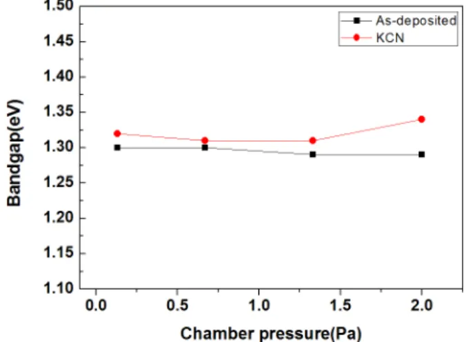
2=0. The bandgaps of as-deposited CIGS films and KCN teated CIGS films are shown in Fig. 6.
The bandgaps of the as-deposited CIGS films showed little change with increasing working pressure, maintaining values close to 1.3 eV. On the other hand, the bandgap of KCN treated CIGS films increased compared to as-deposited CIGS films.
The increase in bandgap is attributed to an increase of the film transmittance which results from the decrease of the scattering by the removal of small Cu-Se particles. The band gaps of Cu-poor films increase by a decrease of the lattice constant due to a reduced p-d hybridization along with lattice deformation
19).
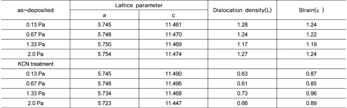
The lattice parameters (a and c) of CIGS films were determined by using the miller indices. The value of lattice parameters, dislocation density and strain (ɛ) of the CIGS films are given in
Fig. 4. SEM micrographs of KCN treated CIGS thin filmsdeposited at various working pressure; (a) 0.13 Pa, (b) 0.67 Pa, (c) 1.33 Pa and (d) 2.0 Pa
Fig. 5. Carrier concentration and resistivity of KCN treated CIGS thin films deposited at various working pressures from 0.13 Pa to 2.0 Pa
Fig. 6. Bandgap of as-deposited and KCN treated CIGS films deposited at various working pressures from 0.13 Pa to 2.0 Pa
Table 2. The value of dislocation density (L) and strain (ɛ) of the deposited CIGS films were calculated by using the eq.(2) and (3)
10).
(2)
and
cos (3)
It was observed that with increasing working pressure, lattice parameters decrease, causing a low angle shift. This low angle shift is directly related to a decrease of Ga atomic percent in the CIGS films at high pressures (Table 1). By KCN treatment, the lattice parameters, dislocations and strains of the CIGS films decreased, suggesting that the CIGS films crystallites were rearranged.
Fig. 7 shows the conductivity of CIGS films deposited on a Mo substrate compared with as-deposited and KCN treated
CIGS films. The as-deposited CIGS films possess high conductivity but after KCN treatment it was decreased by an order of 10
0Ω
-1cm
-1. The Cu content in the film exert a strong influence on the electrical properties and the device performance. Cu-rich CIGS films have negative effect on the properties of the film, decreasing the cell efficiency; while Cu relatively poor films
Table 1. Composition of as-deposited and KCN treated CIGS thin films deposited at various working pressuresAs-deposited Cu In Ga Se Cu/III Ga/III Se/Cu
0.13 Pa 27.27 17.09 7.58 48.06 1.11 0.31 1.76
0.67 Pa 27.17 17.78 7.51 47.54 1.07 0.30 1.75
1.33 Pa 26.40 18.34 7.11 48.15 1.04 0.28 1.82
2.0 Pa 27.20 17.82 6.80 48.17 1.10 0.28 1.77
KCN treatment
0.13 Pa 23.83 19.17 7.11 49.89 0.91 0.27 2.09
0.67 Pa 22.85 20.21 6.90 50.04 0.84 0.26 2.19
1.33 Pa 23.55 20.06 6.69 49.70 0.88 0.25 2.11
2.0 Pa 23.17 20.67 7.00 49.16 0.84 0.25 2.12
Table 2. Lattice parameter, dislocation density and strain of as-deposited and KCN treated CIGS thin films at various working pressure
as-deposited Lattice parameter
Dislocation density(L) Strain(ε)
a c
0.13 Pa 5.745 11.461 1.28 1.24
0.67 Pa 5.748 11.470 1.24 1.22
1.33 Pa 5.750 11.469 1.17 1.19
2.0 Pa 5.754 11.474 1.27 1.24
KCN treatment
0.13 Pa 5.745 11.490 0.63 0.87
0.67 Pa 5.748 11.496 0.61 0.85
1.33 Pa 5.734 11.468 0.73 0.96
2.0 Pa 5.723 11.447 0.66 0.89
Fig. 7. Conductivity of as-deposited and KCN treated CIGS films deposited on Mo film at various working pressure
(Cu/III ratio range of 0.75 to 0.98) have positive effects on the properties of CIGS film.
4. Conclusions
CIGS thin films of 1 μm in thickness were deposited using single quaternary target by one-step RF magnetron sputtering on Mo coated soda lime glasses. The composition and electrical properties of the CIGS films deposited at different working pressures were investigated. The resistivity of CIGS films varies from 10
0to 10
-1Ωcm with increasing working pressure. Also all CIGS films showed a preference for the (112) orientation.
The existence of a Cu-Se secondary phase within CIGS films revealed that the Cu concentrations near the film surface significantly increased. After KCN treatment, the resistivity of the CIGS films increased by a factor of 10
1Ωcm; while the CIGS film surface became smooth and flattened. Measurements of the as-deposited CIGS films revealed that the Cu/III ratio was high enough to be considered that the films was Cu-rich. The excess of Cu was removed from the CIGS films by KCN treatment, achieving a suitable Cu concentration (referred as Cu-poor) for the fabrication of solar cell. Due to high Cu concentrations on the CIGS film surface induced by Cu-Se phases after CIGS film deposition, KCN treatment proved to be necessary for the fabrication of high efficiency solar cells. Also during KCN treatment, dislocation density and lattice parameter decreased as excess Cu was removed, resulting in increase in bandgap and the decrease in the conductivity of CIGS films. It was revealed that by KCN wet etching of CIGS films, Cu-Se secondary phase could be removed, allowing the fabrication of high efficiency absorber layer.
Acknowledgments
This work was supported by the Pioneer Research Program (2011-0002123) through the National Research Foundation funded by the Ministry of Education, Science, and Technology, Korea.
References
1. I. Repins, M. A. Contreras, B. Egaas, C. Hehart, J. Scharf, C. L.
Perkins, B, To and R. Noufi, “19.9%-efficient ZnO/CdS/
CuInGaSe2 solar cell with 81.2% fill factor”, Prog. Photovolt : Res. Appl, Vol. 16, pp. 235-239, 2008.
2. P. Jackson, D. Hariskos, E. Lotter, S. Paetel, R. Wuerz, R.
Menner, W. Wischmann, M. Powalla, “New world record effi- ciency for Cu(In,Ga)Se2 thin-film solar cells beyond 20%”, Prog. Photovoltaics: Res. Appl., Vol. 19, pp. 894-897, 2011.
3. Hui Kong, Jun He, Ling Huang, Liping Zhu, Lin Sun, Pingxiong Yang, Junhao Chu, “Effect of working pressure on growth of Cu(In,Ga)Se2 thin film deposited by sputtering from a single quaternary target”, Materials Letters, Vol. 116, pp.
75-78, 2014.
4. C. Guillen, J. Herrero, “Improvement of the optical properties of electrodeposited CuInSe2 thin films by thermal and chemical treatments”, Solar Energy Materials and Solar Cells, Vol. 43, pp. 47-57, 1996.
5. S. Taunier, J. Sicx-Kurdi, P. P. Grand, A. Chomont, O.
Ramdani, L. Parissi, P. Panheleux, N. Naghavi, C. Hubert, M.
Ben-Farah, J. P. Fauvarque, J. Connolly, O. Roussel, P.
Mogensen, E. Mahe, J. F. Guillemoles, D. Lincot and O.
Kerrec, “Cu(In,Ga)(S,Se)2 solar cells and modules by electro- deposition”, Thin Solid Films, Vol. 480-481, pp.526-531, 2005.
6. Shirakawa S, Kannaka Y, Hasegawa H, Kariya T, Isomura S.,
“ Properties of Cu(In,Ga)Se2 thin films prepared by chemical spray pyrolysis”, Jpn J.Appl. Phys., Vol. 38, pp.4997, 1999.
7. Lin PY, Fu YH, “Fabrication of CuInSe2 light absorption mate- rials from binary precursors via wet chemical process”, Mater Lett., Vol. 75, pp. 65-67, 2012.
8. Seon Mi Kong, Rong Fan, Sung Hee Jung, Chee Won Chung,
“Characterization of Cu(In,Ga)Se2 thin films prepared by RF magnetron sputtering using a single target without seleniza- tion”, Journal of Industrial and Engineering Chemistry, Vol.
19, pp. 1320-1324, 2013.
9. Sung Hee Jung, Rong Fan, Wan In Lee, Chee Won Chung,
“Structural and electrical properites of radio frequency magnet- ron sputtered Cu(InxGa1-x)Se2 thin films with additional post- heat treatment”, Thin Solid Films, Vol. 547, pp. 86-90, 2013.
10. P. K. Mishra, V. Dave, R. Chandra, J. N. Prasad, A. K.
Choudhary, “Effect of processing parameter on structural, opti- cal and electrical properties of photovoltaic chalcogenide nano- structured RF magnetron sputtered thin absorbing films”, Materials Science in Semiconductor processing, in press, 2014.
11. C. H. Chen, T. Y. Lin, C. H. Hsu, S. Y. Wei, C. H. Lai,
“Comprehensive characterization of Cu-rich Cu(In,Ga)Se2 ab- sorber prepared by one-step sputtering process”, Thin Solid Films, Vol. 535, pp. 122-126, 2013.
12. X. Huang, X. Miao, N. Yu, X. Guan, “Effects of deposition profiles on RF-sputtered Cu(In,Ga)Se2 films at low substrate temperature”, Applied Surface Science, Vol. 287, pp. 257-262, 2013.
13. Z. Yu, L. Liu, Y. Yan, Y. Zhang, S. Li, C. Yan, Y. Zhang, Y.
Zhao, “Properties of different temperature annealed Cu(In,Ga)Se2 and Cu(In,Ga)2Se3.5 films prepared by RF sputtering”, Applied Surface Science, Vol. 261, pp. 353-359, 2012.
14. M. A. Contreras, K. M. Jones, L. Gedvials, R. Matson,
“Preferred orientation in polycrystalline Cu(In,Ga)Se2 and its effect on absorber thin-films and devices”, Proc. 16th Eur.
Photovolt. Solar Energy Conf., Vol. 732, 2001.
15. A. J. Zhou, D. Mei, X. G. Kong, X. H. Xu, L. D. Feng, X. Y.
Dai, T. Gao, J. Z. Li, “One-step synthesis of Cu(In,Ga)Se2 ab- sorber layers by magnetron sputtering from a single quaternary target”, Thin Solid Films, Vol. 520, pp. 6068-6074, 2012.
16. J. L. Hernandez-Rojas, M. L. Lucia, I. Martil, G. Gonzalez- Diaz, J. Santamaria, F. Sanchez- Quesada, “Stoichiometry control over a wide composition range of sputtered CuGaxIn(1-x)Se2”, Appl. Phys. Lett., Vol. 64, pp. 1239-1241, 1994.
17. Z. Yu, C. Yan, Y. Yan, Y. Yan, Y. Zhang, T. Huang, W.
Huang, S. Li, L. Liu, Y. Zhang, Y. Zhao, “Effect of annealing temperature on properties of RF sputtered Cu(In,Ga)Se2 thin films”, Applied Surface Science, Vol. 258, pp. 8527-8532, 2012.
18. Z. Yu, C. Yan, T. Huang, W. Huang, Y. Yan, Y. Zhang, L. Liu, Y. Zhang, Y. Zhao, “Influence of sputtering power on composition, structure and electrical properties of RF sputtered CuIn1-xGaxSe2
thin films”, Applied Surface Science, Vol. 258, pp. 5222-5229, 2012.
19. S. H. Han, F. S. Hasoon, and J. W. Pankow, A. M. Hermann, D. H. Levi, “Effect of Cu deficiency on the optical bowing of chalcopyrite CuIn1-xGaxSe2”, Applied physics letters, Vol. 87, pp. 151904-1-3, 2005.