http://dx.doi.org/10.5369/JSST.2019.29.1.14 pISSN 1225-5475/eISSN 2093-7563
NO 2 Sensing Characteristics of Si MOSFET Gas Sensor Based on Thickness of WO 3 Sensing Layer
Yujeong Jeong
1, Seongbin Hong
1, Gyuweon Jung
1, Dongkyu Jang
1, Wonjun Shin
1, Jinwoo Park
1, Seung-Ik Han
2, Hyungtak Seo
2,3, and Jong-Ho Lee
1+Abstract
This study investigates the nitrogen dioxide (NO
2) sensing characteristics of an Si MOSFET gas sensor with a tungsten trioxide (WO
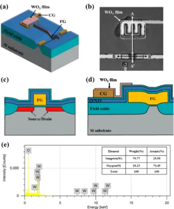
3) sensing layer deposited using the sputtering method. The Si MOSFET gas sensor consists of a horizontal floating gate (FG) inter- digitated with a control gate (CG). The WO
3sensing layer is deposited on the interdigitated CG-FG of a field effect transistor(FET)- type gas sensor platform. The sensing layer is deposited with different thicknesses of the film ranging from 100 nm to 1 µm by changing the deposition times during the sputtering process. The sensing characteristics of the fabricated gas sensor are measured at different NO
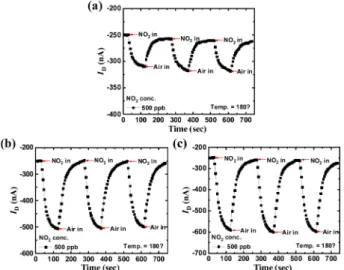
2concentrations and operating temperatures. The response of the gas sensor increases as the NO
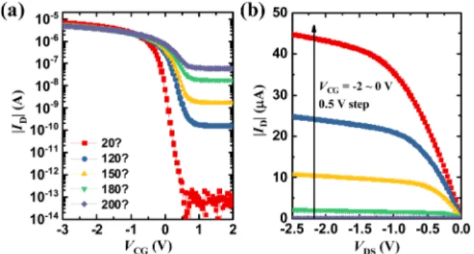
2concentration and operating temperature increase. However, the gas sensor has an optimal performance at 180
oC considering both response and recovery speed. The response of the gas sensor increases significantly from 24% to 138% as the thickness of the sensing layer increases from 100 nm to 1 µm. The sputtered WO
3film consists of a dense part and a porous part. As reported in previous work, the area of the porous part of the film increases as the thickness of the film increases. This increased porous part promotes the reaction of the sensing layer with the NO
2gas.
Consequently, the response of the gas sensor increases as the thickness of the sputtered WO
3film increases.
Keywords: Gas sensors, WO
3, FET-type, NO
2gas, RF magnetron sputtering
1. INTRODUCTION
Deterioration in the quality of indoor and outdoor air exposes people to noxious gases. Among such gases are nitrogen and sulfur oxides emitted by automobiles and from the combustion of fossil fuels. In view of resolving this issue, several studies have been conducted on gas sensing technologies that can detect noxious gases. Studies conducted to date have led to various types of gas sensors, such as optical-, electrochemical-, and semiconductor sensors, which have also met the requirements for
low cost, low power consumption, and high reliability [1-7].
Optical gas sensors detect the gas based on the phenomenon that the intensity of a light source changes when the gas adsorbs the light [1-2]. Optical gas sensors have the advantages of fast response time and good selectivity; however, they are limited by their large size and high cost. Electrochemical gas sensors detect gas molecules based on the phenomenon that the conductance of an electrolyte changes when it reacts with the target gas molecules [3-5]. The advantages of electrochemical gas sensors are higher sensitivity and lower prices in comparison with optical gas sensors. However, electrochemical gas sensors are not reliable because the electrolytes in them dry under the conditions of high temperature and low humidity conditions [3-4]. The field effect transistor (FET)-type is another gas sensor that has been studied.
These sensors have the advantages of small size, low power consumption, and compatibility with the complementary metal- oxide-semiconductor (CMOS) process [6-7]. The FET-type gas sensor proposed in our previous study has a high coupling ratio, because it has a horizontal floating gate (FG) interdigitated with a control gate (CG) [8-9]. FET-type gas sensors are compatible with the CMOS process because contamination cannot occur during the formation of the sensing layer in the sensor.
In previous studies on the gas sensor with the WO
3sensing
1
Department of Electrical Engineering, and Inter-University Semiconductor Research Center, Seoul National Unversity, 1 Gwanakro, Gwanak-gu, Seoul 08826, Korea
2
Department of Energy Systems Research, Ajou Unversity, 206 World cupro, Yeongtong-gu, Suwon 16499, Korea
3
Department of Materials Science and Engineering, Ajou Unversity, 206 World cupro, Yeongtong-gu, Suwon 16499, Korea
+