DOI: http://dx.doi.org/10.4313/JKEM.2013.26.6.441
a-, c-, m-면방향의 4H-SiC 기판에 형성된 ZnO 나노선 가스센서의 300℃에서 CO 가스 감지 특성
정경환1, 이정호1, 강민석1, 구상모1,a
1 광운대학교 전자재료공학과
CO Gas Sensing Characteristic of ZnO Nanowires Based on the a-, c- and m-plane Oriented 4H-SiC Substrate at 300℃
Gyeong-Hwan Jeong1, Jung-Ho Lee1, Min-Seok Kang1, and Sang-Mo Koo1,a
1 Department of Electrical Materials Engineering, Kwangwoon University, Seoul 139-701, Korea
(Received December 10, 2012 : Revised February 16, 2013; Accepted May 24, 2013)
Abstract: ZnO nanowires on the a-, c- and m-plane oriented 4H-SiC substrates were grown by using a high temperature tube furnace. Ti/Au electrodes were deposited on ZnO nanowires and a-, c- and m-plane 4H-SiC substrates, respectively. The shape and density of the ZnO nanowires were investigated by field emission scanning electron microscope. It was found that the growth direction of nanowires depends strongly on growth parameters such as growth temperature and pressure. In this work, The sensitivity of nanowires formed a-, c- and m-plane oriented 4H-SiC gas sensor was measured at 300℃ with CO gas concentration of 80%. The nanowires grown on a-plane oriented 4H-SiC show improved sensing performance than those on c- and m-plane oriented 4H-SiC due to the increased density of nanowire on a-plane 4H-SiC.
Keywords: 4H-SiC, CO gas sensor, Nanowire, Substrate orientation
1. 서 론
ZnO는 상온에서 높은 밴드갭 에너지 (∼3.4 eV)와 엑시톤 결합 에너지 (60 meV)를 가진다. 특히, ZnO 나노선 구조는 박막보다 넓은 표면적대부피비 때문에 가스 센서에 많이 응용된다 [1,2]. 4H-SiC는 ZnO와 같은 Hexagonal 구조를 가짐으로 낮은 격자부정합 (lattice mismatch)을 가지며, 고에너지 밴드갭 반도체 물질로 높은 화학적 비반응성을 가진다. 또한 고온에
a. Corresponding author; [email protected] Copyright ©2013 KIEEME. All rights reserved.
This is an Open-Access article distributed under the terms of the Creative Commons Attribution Non-Commercial License (http://creativecommons.org/licenses/by-nc/3.0) which permits unrestricted non-commercial use, distribution, and reproduction in any medium, provided the original work is properly cited.
서도 반도체 성질을 잃지 않기 때문에 고온 환경에서 동작해야 하는 가스센서에 응용이 가능하여 국내외적 으로 많은 관심을 갖고 있다 [3-5].
현재까지의 가스센서 연구는 나노입자를 이용한 것 이 대부분이었지만, 최근에는 높은 비표면적, 우수한 결정성, 나노스케일의 크기 등 다양한 물리, 화학적 특성을 지닌 1차원 나노구조체를 이용한 가스센서 연 구가 활발히 진행되고 있다. 하지만 기판의 결정면 방향 제어 및 의존 특성 연구에 대한 연구는 매우 미 흡한 상황이다.
따라서 본 연구에서는 4H-SiC의 a-, c-, m-면방향 에 따른 300℃에서의 CO 가스에 대한 감도를 측정하 여 감도 특성 개선을 위한 연구를 수행하고, 분석 검 토하였다.
2. 실험 방법
그림 1(b)는 ZnO 나노선/SiC 가스센서의 모식도 이다. p형 4H-SiC 기판을 아세톤, 메탄올, DI water, SPM (sulfuric acid peroxide mixture), DI water, BOE (buffered oxide etchant), DI water 순서로 기 판을 세척하였다. 세척 후 Au 10 nm를 E-beam 공정 으로 증착하고 1,200℃인 튜브 퍼니스에서 비율 ZnO : Graphite = 1 mg : 1 mg인 소스를 사용하여 60분 동안 기판에 증착하여 ZnO 나노선을 형성하였다. 그 후 Ti 50 nm 전극 층과 Au 50 nm 전극층을 E-beam 증착 공정으로 형성하였다.
Fig. 1. Schematic diagram of (a) gas sensor measurement system, (b) ZnO nanowire/SiC gas sensor.
형성된 ZnO 나노선의 특성은 FE-SEM (field emission scanning electron mmicroscope), PL (photoluminescence) 과 AFM (atomic force microscope)을 이용하여 분석하였 다. 가스 센서의 감도 측정은 그림 1(a)와 같은 가스 센 서 측정 장치를 이용하였다. a-, c-, m-면방향 4H-SiC 기반의 나노선 가스 센서는 air pump, CO pump와 연결 된 챔버 안에 놓은 후, 전류를 1 μA로 고정시킨 후, 300℃인 상태에서 CO 80% 환경에서 1,200초, 공기 100% 환경에서 600초 동안 저항을 측정하였다.
3. 결과 및 고찰
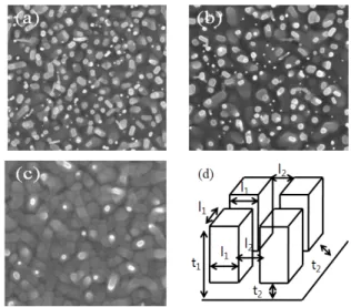
그림 2는 ZnO 나노선의 FE-SEM 이미지와 유효 두께를 구하기 위한 매개 변수를 보여주는 기하학적 구조이다. (a)는 a-면방향, (b)는 c-면방향, (c)는 m-면방향
Fig. 2. Top view FE-SEM images of ZnO nanowires grown on (a) a-plane oriented, (b) c-plane-oriented, (c) m-plane oriented 4H-SiC substrates and Geometric model of nanowire structure showing parameters to estimate effective thickness.
Fig. 3. AFM images of ZnO nanowires grown on (a) a-plane oriented, (b) c-plane-oriented, (c) m-plane oriented 4H-SiC substrates.
나노선/SiC를 나타낸다. FE-SEM 이미지를 통해 a- 면방향 의 나노선 밀도가 가장 높으며, c-, m-면방향 순으로 밀도가 높게 나타남을 보았다. 기판 면방향에
Table 1. Effective thickness of ZnO nanowires grown on a-, c- and m-plane oriented 4H-SiC substrates.
Substrate
orientation a-plane c-plane m-plane
t1 7,19 μm 4.03 μm 3.04 μm
t2 0.20 μm 0.20 μm 0.20 μm
l1 0.74 μm 0.805 μm 0.54 μm
l2 1.41 μm 2.45 μm 6.80 μm
tln (equation a) 0.10 μm 0.06 μm 0.02 μm
따른 ZnO 나노선의 밀도가 다른 이유는 기판 표면의 에너지가 면방향에 따라 다르기 때문이라 판단된다 [2].
그림 2(d)는 나노선의 유효 두께를 구하기 위한 매 개 변수를 보여주는 기하학적 구조이다. SEM 이미지 를 통하여 t1, t2, l1, l2를 구한 후, 식 (1)을 사용하여 유효 두께를 구하였다 [6].
ln≈
(1)
면방향에 관계없이 t2의 값은 같고, t1, l1, l2 값에 따라 유효 두께값은 a-, c-, m-면방향 순으로 높게 나왔다. 유효 두께값은 표 1에 정리하였다.
그림 3은 ZnO 나노선의 AFM 사진이다. (a)는 a- 면방향, (b)는 c-면방향 (c)는 m-면방향 ZnO 나노선 /SiC이다. 나노선의 경우 박막과 달리 직접적으로 표 면 거칠기를 구할 수 없어, AFM 이미지를 통하여 표 면 거칠기를 구하였다 [7].
S N
i
N
Zi Za
(2)
식 (2)는 표면거칠기를 구하는 식으로, Zi는 픽셀 i 에서의 이미지 높이이며, Za는 평균 높이이고, N은 AFM 이미지에서 픽셀의 수이다. a-면방향 표면 거 칠기는 217.23 nm이고, c-면방향 표면 거칠기는 122.72 nm이며, m-면방향 표면거칠기는 72.06 nm으 로 표 2에 정리하였다. ZnO 나노선의 밀도가 증가할 수록 ZnO 나노선의 표면 거칠기가 증가됨을 확인하 였다.
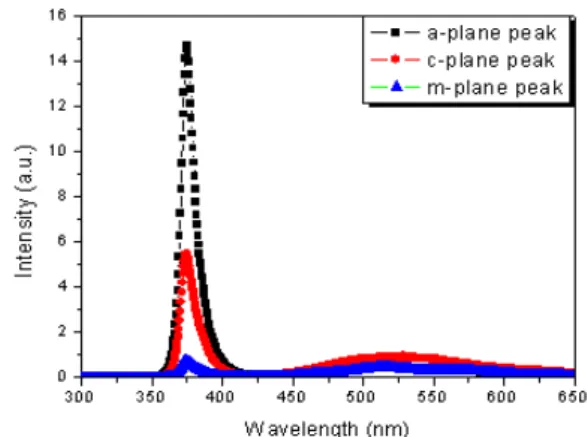
Fig. 4. Photoluminescence spectrum of ZnO nanowires grown on a-, c-, and m-plane oriented 4H-SiC substrates.
Fig. 5. CO gas sensitivity of ZnO nanowires based on the a-, c- and m-plane 4H-SiC.
그림 4는 a-, c-, m-면방향 기판에 형성된 ZnO 나 노선의 photoluminescence 측정 결과이다. ZnO 나노 선의 PL 특성 파장은 374 nm (∼3.3 eV)로 같으며, photoluminescence 세기는 a-면방향 14.7 a.u., c-면방 향 5.49 a.u., m-면방향 0.73 a.u.으로 측정되었다.
ZnO 나노선의 밀도와 표면 거칠기가 증가할수록 부 피대표면적 비율이 커지며, PL의 세기도 m-, c-, a- 면방향 순으로 증가하였다.
그림 5는 300℃에서 가스센서에 1 uA의 고정전류를 흘려주면서 CO 가스 농도 80%인 경우 ZnO 나노선 /SiC 가스센서의 저항을 측정하여 감도로 변환한 결과 이다. 센서 감도를 구하는 식은 식 (3)에 나타내었다.
Table 2. Surface roughness, photoluminescence and sensitivity of ZnO nanowires grown on a-, c- and m-plane oriented 4H-SiC substrates.
Substrate orientation
Surface Roughness(nm)
Photolumine scence(a.u.)
Sensitivit y(%)
a-plane 217.23 14.70 31.67
c-plane 122.72 5.49 19.38
m-plane 72.06 0.73 6.04
× (3)
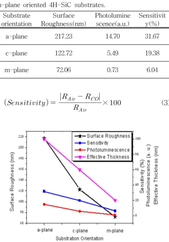
Fig. 6. Surface roughness dependent to sensitivity, photoluminescence and effective thickness.
RAir는 공기환경에서 가스 센서의 저항이며, RCO는 CO 가스 환경에서 가스 센서의 저항이고, (sensitivity)는 감도이다. 공기 환경에서 산소가 ZnO 표면에 흡착되어 가스 센서의 저항이 증가하고, CO 가스 환경에서 ZnO 표면의 산소가 CO 가스와 반응 하여 ZnO 표면에서 탈착되어 가스 센서의 저항이 감 소하기 때문에 공기 환경에서 CO 환경으로 변하면 시간에 따라 가스 센서의 감도가 변하게 된다. ZnO 표면에서 흡착/탈착 되는 산소의 양이 많을수록 가스 센서의 감도는 크다. a-면방향 감도는 31%이며, c-면 방향 감도는 19%이고, m-면방향 감도는 6%로 표 2 에 정리하였다. 흡착/탈착되는 산소의 양은 표면 거칠 기에 비례하며, 표면 거칠기가 높을수록 감도가 높게 나타남을 확인하였다.
그림 6은 a-, c-, m-면방향 ZnO 나노선/SiC의 표
면 거칠기, PL 세기, 감도, 유효 두께를 비교한 그래 프이다. 표면 거칠기와 PL의 세기, 유효두께, 감도는 모두 비례하여 나타났다. a-면방향 ZnO 나노선/SiC 가스센서의 감도가 c-면방향 ZnO 나노선/SiC 가스센 서 보다 약 1.5배, m-면방향 ZnO 나노선/SiC 가스센 서의 감도보다 약 5배 가량 높게 나타났다.
4. 결 론
본 연구에서는 p형 4H-SiC 기판에 형성된 a-, c-, m-면방향 ZnO 나노선 가스센서의 CO 감지 특성을 300℃에서 조사하였으며, FE-SEM을 통해 a-, c-, m-면방향 ZnO 나노선이 형성됨을 확인하였고, 유효 두께는 a-면방향 0.1 μm, c-면방향 0.06 μm, m-면방 향 0.02 μm임을 확인하였다. ZnO 나노선의 표면 거 칠기는 a-, c-, m-면방향 기판에 형성된 나노선 순서 로 217.23 nm, 122.72 nm, 72.06 nm이고, PL 특성 파 장은 374 nm (∼3.3 eV)이고 세기는 14.7 a.u., 5.49 a.u., 0.73 a.u.이며, 감도는 31.67%, 19.68%, 6.04%으 로 a-면방향 나노선/SiC 가스 센서의 감도가 c-, m- 면방향 나노선/SiC 감도보다 높은 특성을 보여주었 다.
본 연구를 통해 SiC 기판 면방향이 성장하는 나노 선의 유효 두께 및 거칠기에 영향을 미치는 것을 확 인 하였으며, 나노선/SiC 기반 고온 가스센서 소자 구조 최적화에 적용 가능할 것이다.
감사의 글
본 연구는 2013년 정부 (교육과학기술부)의 재원으로 한국연구재단의 지원 (2010-0011022 및 2012M2B2A4029) 및 광운대학교의 지원에 의한 것입니다.
REFERENCES
[1] D. T. Phan and G. S. Chung, Appl. Surf. Sci., 257, 8 (2001).
[2] I. J. Kim, B. H. Oh, J. H. Lee, and S. M. Koo, J.
KIEEME, 25, 91 (2012).
[3] D. D. Lee and D. S. Lee, IEEE Sensors J., 1, 214 (2001).
[4] H. W. Ra, K. S. Choi, J. H. Kim, Y. B. Hahn, and Y.
H. Im, Small, 4, 1105 (2008).
[5] E. Janzen and O. Kordina, Mater. Sci. Eng., B46, 203 (1997).
[6] M. M. Steeves, D. Deniz, and R. J. Lad, Appl. Phys.
Lett., 96, 142103 (2010).
[7] J. W. Elam, Z. A. Sechrist, and S. M George, Thin Solid Films, 414, 43 (2002).
[8] E. Karber, T. Raadik, T. Dedova, J. Krustok, A.
Mere, V. Mikli, and M. Krunks, Nanoscale Reserch Letters, 6, 359 (2011).