• 검색 결과가 없습니다.

Analysis of Planar Metal Plasmon Waveguides

N/A
N/A
Protected

Academic year: 2021

Share "Analysis of Planar Metal Plasmon Waveguides"

Copied!
6
0
0

로드 중.... (전체 텍스트 보기)

전체 글

(1)

Analysis of Planar Metal Plasmon Waveguides

Jaehoon Jung

Department of Electronics and Electrical Engineering, Dankook University

ABSTRACT

Propagation modes of symmetric metal-insulator-metal SPP waveguides are analyzed. Main characteristics of these waveguides such as mode effective index, propagation length, and penetration depths are calculated at the telecom wavelength for different layer thickness. We adopt Au, Al as a metal material and air, glass as a dielectric material and obtain different optical characteristics. The surface plasmon characteristics in this paper provide a numerical insight for designing nanostructure metal plasmon waveguide.

Key Words : Surface Plasmon Polariton (SPP), circular waveguide, optimal design.

1. Introduction

Surface plasmon polaritons (SPPs) are electromag- netic excitations that are coupled to surface plasmon (surface plasma oscillation) and propagate along metal-dielectric interfaces [1]. SPP optics has been an area of active research and its applications include opti- cal devices for coupling, confining, and guiding in nanometer scale [2]. Plasmonic waveguides with sub- wavelength field profile have been proposed and ana- lyzed [3-5]. Recently, SPP gap waveguides whose core is thin dielectric and cladding is metal have been sug- gested and various structures have been modeled [6,7].

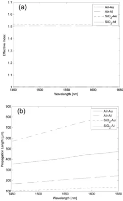
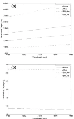
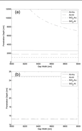
In this paper, we discuss fundamental characteris- tics of SPP waveguide structures with a thin dielectric layer surrounded by metal, that is, symmetric metal- insulator-metal (MIM). For the effective index, prop- agation length, and penetration depths which are criti- cal for designing photonic devices with subwavelength dimension, we present some computational results for different dielectric and metal materials.

2. Surface Plasmon polaritons (SPPs) at metal-air single interface

Fig. 1 shows the wavelength dependence of dielec-

tric constant (the real part in (a) and the imaginary part in (b)) of Au and Al at telecommunication wave- lengths (1450-1650 nm) [8]. SPP waveguides needs one or more metal-dielectric interface. In this paper,

E-mail : [email protected]

Fig. 1. The real (a) and imaginary (b) parts of dielectric

constants of Au and Al [8].

(2)

we employ Au, Al as a metal material and air, glass as a dielectric material since they are frequently used as a SPP material and have much different permittivity values. Over the wavelength range of interest, both of the real and imaginary parts of Au are smaller than that of Al in magnitude.

We now consider SPP propagating along an inter- face consisting of a dielectric material (e

d

) and a metal with complex dielectric function (e

m

) as shown in Fig. 2(a).

The interface between semi-infinite materials hav- ing positive and negative dielectric constants can only transverse magnetic (TM) surface waveguide [4]. The electric field has only y component (Ey) and can be expressed in the form

(1)

where b is the complex propagation constant β=β'- iβ'', which is related to the mode effective index according to β'=k

0

n

eff

and propagation length defined as L

sp

=1/(2β'') with k

0

propagation constant at air. The penetration depths in metal and dielectric are defined in Fig. 2(b), respectively. SPP waveguids have advan- tage of sharp confinement over dielectric ones, and

thus, the penetration depths are among primary param- eters.

The dispersion equation of SPP at a single interface can be expressed as

. (2)

In Fig. 3(a), (b) we show, respectively the effective index n

eff

and propagation length L

sp

of SPP mode calculated using Eq. (2). We can see that the effective index increases and the propagation length decreases when we use large-refractive index dielectric and small -magnitude dielectric function metal.

Fig. 4 shows the penetration length of SPP modes in dielectric (a) and metal (b), respectively as defined in Fig. 2(b). We observe that the effective index increases with the refractive index of dielectric mate- rial and decreases with magnitude of dielectric func- tion of metal, and the propagation length has contrary trend. It is interesting that the penetration depths in E = E y ( ) exp [ i ω t βz ( – ) ]

β ε

d

ε

m

( ) ω ε

d

+ ε

m

( ) ω ---k

0

=

Fig. 2. (a) Schematic representation of a single dielectric material and metal. (b) penetration depths in the dielectric material and in the metal.

Fig. 3. (a) The calculated effective index (b) propagation

length for a metal-air interface.

(3)

metals depends rather weakly on the wavelength staying at the level of a few tens of nanometers, while that in dielectrics increases fast and nonlinearly with the wavelength.

3. Gap SPP Symmetric mode

Considering the SPP modes associated with two symmetric metal-dielectric interfaces, a dielectric layer surrounded by metals as shown in Fig. 5, there are two propagating modes, symmetric and anti-sym- metric mode [4]. Note that the symmetric mode means the symmetric transverse electric field compo- nent about the horizontal axis passing through the center of the dielectric layer. As shown in Fig. 6, propagation modes in gap SPP waveguide with gold and glass, split into two of which one has symmetric (even) transverse electric field profile E

y

, and the other anti-symmetric(odd) one. The effective index of even mode increases to infinity, while that of odd mode has a cutoff thickness.

Now, we calculate primary SPP parameters of the symmetric mode with gap thickness h with a fixed wavelength. In the simulation results presented hear- after, an excitation wavelength λ=1550 nm, Au(ε

m

= -95.924+10.968i), Al(ε

m

=-253.93+46.08i), glass(n=1.5), and air(n=1) are used. It can be immediately seen that the effective index of the waveguide decreases and the propagation length increases with the thickness of dielectric layer.

In Fig. 7(a), (b), we show respectively the effective index n

eff

and propagation length L

sp

of symmetric SPP mode supported MIM waveguide. It is expected that the effective index is monotonic decreasing with gap width and the order in value does not change.

Furthermore, the effective index is big when the refractive index of dielectric is large and the magni- tude of dielectric function of metal is small. At larger gap width, we can also see that the propagation length Fig. 4. The calculated penetration depths (a) in the dielectric

and (b) in the metal.

Fig. 5. Schematic representation of a metal-insulator-metal (MIM) waveguide.

Fig. 6. Propagation modes (symmetric and anti-symmetric)

in MIM SPP waveguide.

(4)

is small when the refractive index of dielectric is large and the magnitude of dielectric function of metal is small, in accordance with the general consideration.

This, however, is not strictly true in the overall range as shown in the range 20-100 nm in Fig. 7(b). This feature arises from the fact that the order of the con- finement in the interface and propagation loss in the metal is always the same.

Fig. 8 (a), (b) show the penetration depths vs. gap width for several metals in the dielectric and metal, respectively. From this figure, it is known that the penetration depths in metals depends rater weakly on the dielectric layer thickness staying at the level of a few tens of nanometers, while that in dielectrics increases fast and nonlinearly with the thickness.

The results presented here show that larger effective index cause shorter penetration depth in dielectric and this is strictly true in the gap width range of interest.

4. Gap SPP Anti-symmetric Mode

From fig. 9(a), (b), we see that the anti-symmetric mode has a cutoff thickness, 3.12λ, 5.14λ, 1.378λ, 2.276λ, in air-Al, air-Au, glass-Au, and glass-Al, respectively. In Fig. 7(a), (b) we show, respectively the effective index n

eff

and propagation length L

sp

of anti-symmetric SPP mode supported MIM waveguide.

We can see that the effective index is big and the propagation length is small when the refractive index of dielectric is large and the magnitude of dielectric function of metal is small.

Fig. 10. (a), (b) show the penetration depths vs.

gap width for several metals in the dielectric and metal, respectively. From this figure, it is known that the penetration depths in metals depends rater weakly on the dielectric layer thickness staying at the level of a few tens of nanometers, while that in dielectrics increases fast and nonlinearly with the thickness.

Fig. 7. (a) The Gap SPP effective index (b) propagation length of symmetric mode as a function of the width of air gap in metal.

Fig. 8. The penetration depths of the symmetric mode (a)

in the dielectric and (b) in the metal as a function

of the width of air gap in metal.

(5)

5. Conclusions

The characteristics of symmetric MIM SPP waveguide configuration have been considered in detail. We calculated effective index, propagation length, and penetration depth for the waveguide structures with single dielectric-metal interface and MIM at telecommunication wavelengths. The metals such as Ag, Au, Al, and Cu were adapted and the val- ues of dielectric constants were employed using Palik data instead of the simple Drude model. It has also been found that for each dielectric layer, the results presented here can be used for choosing appropriate materials for metal and dielectric for optimal parame- ters of MIM including mode effective index, and propagation length, penetration depths in dielectric and metals. We believe that the our results enhance our understanding of main features of SPP guiding in symmetric MIM structures as well as afford useful guidelines for designing MIM-based components.

Acknowledgement

The present research was conducted by the research fund of Dankook University in 2009.

References

1. H. Reather, Suface Plasmons, Springer Tracts in Mod- ern Physics, Springer Berlin, 1988.

2. W. L. Barnes, A. Dereux, and T. W. Ebbesen, “ Sur- face Plasmon Subwavelength Optics,” Nature, vol.

424, pp.824-830, 2003.

3. Stefan A. Maier, “Plasmonics: The Promise of Highly Integrated Optical Devices,” IEEE J. of Selected Top- ics in Quantum Electronics, Vol. 12, No. 6, pp. 1671- 1677, 2006.

4. P. Berini, “Plasmon-polariton waves guided by thin lossy metal films of finite width: Bound modes of symmetric structures”, Physical Review B, Vol. 61, No. 15, pp. 10484-10503, 2000.

5. A. Hosseini, and Y. Massoud, “A low-loss metal-insu- lator-metal plasmonic Bragg reflector”, Optics Express, Fig. 9. (a) The Gap SPP effective index (b) propagation

length of anti-symmetric mode as a function of the width of air gap in metal.

Fig. 10. The penetration depths of the anti-symmetric mode

(a) in the dielectric and (b) in the metal as a function

of the width of air gap in metal.

(6)

Vol. 14, No. 23, pp. 11318-11323, 2006.

6. K. Tanaka and M. Tanaka, “Simulations of nanomet- ric optical circuits based on surface plasmon polariton gap waveguide,” Appl. Phys. Lett, vol. 82, No. 8, pp.1158-1160, 2003.

7. B. Wang and G. P. Wang, “Metal heterowaveguides for nanometric focusing of light,” Appl. Phys. Lett,

vol. 85, No. 16, pp.3599-3601, 2004.

8. E. Palik , Handbook of Optical Constants of Solids, Academic Press, New York, 1985.

접수일: 2010년 5월 31일, 1차심사일: 2010년 6월 7일

2 차심사일: 2010년 6월 11일, 게재확정일: 2010년 6월 15일

수치

Fig. 1 shows the wavelength dependence of dielec-
Fig. 2. (a) Schematic representation of a single dielectric material and metal. (b) penetration depths in the dielectric material and in the metal.
Fig. 6. Propagation modes (symmetric and anti-symmetric) in MIM SPP waveguide.
Fig. 8 (a), (b) show the penetration depths vs. gap width for several metals in the dielectric and metal, respectively
+2

참조

관련 문서

It is expected to be used for forecasting and analysis of precipitation structure and characteristics of mesoscale system causing heavy rainfall using the

trade deficit has lasted for 20 years, and Japan’s current account surplus has also lasted for 22 years, indicating that the evolution of the current

CMP process is effectively used to flat dielectric layer such as IMD, ILD, PMD and metal layer such as W, Al, Cu in order to perform multi layer

Recently, metal-assisted chemical etching (MACE) has been widely used for the synthesis of SiNWs, because this technique has advantages such as simplicity, low operating

Crosslinker Dabco CL420 Non-fugitive novel cross-linker providing significantly improved humid aged physical properties9. Dabco T-12 Industry standard

• Defenders need visibility into process and file telemetry, command line parameters, and Windows Event logs. • Subscribe to ETW logs to collect PowerShell cmdlets and

Evidence for the acceptability of the Geneva Bible has been found in the fact that its original and revised editions were published and circulated more

“With the MySQL Query Analyzer, we were able to identify and analyze problematic SQL code, and triple our database performance. More importantly, we were able to accomplish