전력 반도체 응용을 위한 HVPE법에 의한 Ga
2O
3에피성장에 관한 연구
Ga
2O
3Epi Growth by HVPE for Application of Power Semiconductors
강 이 구 *★
Ey Goo Kang*★ Abstract
This research was worked about Ga2O3 Epi wafer that was one of the mose wide band gap semiconductors to be used power semiconductor industry. This wafer was grown 5.3㎛ thickness on Sn doped Ga2O3 Substrate by HVPE(Hydride Vapor Phase Epitaxy). Generally, we can fabricate 600V class power semiconductor devices when the thickness of compoound power semiconductor is 5㎛. but in case of Ga2O3 Epi wafer, we can obtain over 1000V class. As a result of J-V measurment of the grown Ga2O3 Epi wafer, we obtain 2.9-7.7mΩ·cm2 on resistance. Specially, in case of reverse, we comfirmed a little leakage current when the reverse voltage is over 200V
요 약
본 논문에서는 최근 전력반도체 산업에서 활용되어지는 와이드밴드갭 반도체 중에 하나인 Ga2O3를 이용한 에피웨이
퍼 성장에 관련되어 서술하였다. GaN 성장시 활용되어지는 HVPE법을 이용하여 Sn이 도핑된 Ga2O3 기판웨이퍼에
평균 5.3㎛ 두께로 성장시켰다. 일반적으로 화합물반도체의 에피 두께가 5㎛일 경우 SiC의 경우 600V 전력반도체
소자를 제작할 수 있으며, Ga2O3 에피웨이퍼의 경우에는 1000V이상의 전력소자를 제작할 수 있다. 성장된 에피웨이
퍼의 J-V 측정 결과 2.9-7.7mΩ·cm2의 온저항을 얻을 수 있었으며, 역방향의 경우 상당히 높은 전압에서도 누설전류가 거의 없음을 알 수 있었다.
Key words : Ga2O3 Substrate, Ga2O3 Epi wafer, Power devices, Wide Band Gap, On resistance
** Dept. of Energy IT Engineering, Far East University
★ Corresponding author
E-mail: [email protected], Tel: +82-43-879-3648
※ Acknowledgment
This research was supported by Korea Institute of Energy Technology Evaluation and Planning(20174010201290) and NRF-2017R1D1A3B03029757
Manuscript received Jun. 12, 2018; revised Jun. 22, 2018; Accepted Jun. 26, 2018
This is an Open-Access article distributed under the terms of the Creative Commons Attribution Non-Commercial License(http://creativecommons.org/licenses/by-nc/3.0) which permits unrestricted non-commercial use, distribution, and reproduction in any medium, provided the original work is properly cited.
Ⅰ. 서론
전력 반도체(power semiconductor)는 전력의 변환이나 제어 등을 수행하는 데 사용되는 반도 체 소자로 정의되며 종류로는 MOSFET, IGBT, BJT, Thyristor 등이 있다. [1]-[3]
또한, 고내압화, 고전류화, 고주파수화 되어 교류와 직류 사이의 변환 효율을 높이는 것뿐만 아니라 세탁기, 냉장고, 청소기, 엘리베이터, 에스 컬레이터에 사용되는 모터를 비롯한 다양한 전자 기기에 전력을 공급하거나 안정적으로 원하는 전압과 전류를 공급할 수 있도록 돕는다. 최근 전기자동차의 큰 이슈로 인하여 자동차용 전력반 도체 (600, 900, 1,200 V)의 수요가 크게 증가하고 있고 산업기기, 철도, 태양전지 분야에서 전력반 도체 모듈의 실용화가 요구되고 있다 [3]-[5].
고전력, 고주파 특성을 갖는 반도체 소자를 구현 하기 위해서는 높은 항복 전압과 동시에 높은 전자이동도를 갖는 반도체 소재가 필요하며, 이에 따르는 열적 안정성도 매우 중요하기 때문에 밴드 갭이 넓은 SiC, GaN, Ga2O3의 필요성이 증대되고 있다.[6]
특히, 갈륨 옥사이드는 4.7 ~ 4.9 eV의 넓은 에 너지 밴드갭을 갖기 때문에 고내압, 저손실 전력 반도체용 소재로 유용하고, SiC, GaN 보다 3배 더 큰 8MeV/cm 항복전계를 갖는 산화물 반도체로서 전력반도체 시장에서 주목받고 있는 소재이다.
따라서 본 논문에서는 차세대 전력 반도체용 소 재로 주목받고 있는 갈륨 옥사이드 에피 성장에 따른 웨이퍼 및 전기적 특성을 분석하여, 전력반 도체 소자로의 응용가능성을 제시하고자 하였다.
Ⅱ. 본론 1. Ga2O3 에피성장
본 논문에서는 HVPE(Hydride Vapor Phase Epitaxy) 성장법을 이용하여 전력반도체 소자로의 응용이 가능한 Ga2O3 에피를 5㎛까지 성장을 시 켰다. 그림 1은 본 연구에서 성장한 Ga2O3 에피웨
Fig. 1. The Structure of Ga2O3 epi wafer.
그림 1. Ga2O3 에피 웨이퍼 구조
Table 1. The property of Ga2O3 epitaxial layer by the method of HVPE growth
표 1. HVPE 성장법에 의한 Ga2O3 에피택셜층의 특성
Property Specification
Dopant Si(n-type)
Doping Concentration order of 1016cm-3
Thickness 5㎛
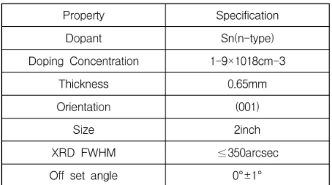
Table 2. The property of Ga2O3 wafer for growth of epitaxial layer
표 2. Ga2O3 에피택셜층의 성장을 위한 웨이퍼의 특성
Property Specification
Dopant Sn(n-type)
Doping Concentration 1-9×1018cm-3
Thickness 0.65mm
Orientation (001)
Size 2inch
XRD FWHM ≤350arcsec
Off set angle 0°±1°
표1에 나타낸 것처럼 에피층의 도펀트는 Si이며, 도핑농도는 1016cm-3 정도를 보여주고 있으며, 표2에서 제시한 에피층 성장을 위한 기판웨이퍼의 특성은 n형 Ga2O3 웨이퍼이며 도핑농도는 1-9×1018cm-3 분포하고 있다.
2. Ga2O3 에피층의 특성
본 절에서는 HVPE 성장법에 의해 성장된 Ga2O3 에피층에 대한 특성을 제시하고 있다.
그림2에서는 성장된 에피택셜 층의 두께 프로파일 을 보여주고 있는데, 웨이퍼의 중심부를 기준으로
Fig. 2. The film thickness mapping of Ga2O3 epitaxial layer 그림 2. Ga2O3 에피층의 필름 두께 프로파일
그림 3에서는 n형 Ga2O3의 표면 농도 프로파일을 보여주고 있으며, 농도파일은 2.0∼5.0×1016cm-3 분 포하고 있으나, 대부분 3×1016cm-3 내외의 균일한 농도파일을 나타내고 있다.
Fig. 3. The donor concentration mapping of Ga2O3 epitaxial layer
그림 3. Ga2O3 에피층의 도너 농도 프로파일
그림 4에서는 성장된 Ga2O3 에피웨이퍼의 활성 화 정도를 파악하기 위한 I-V 측정 지점을 표시 하고 있다. 이러한 I-V 측정을 하기 위해 애노드 전극과 캐소드 전극을 설치하였으며, 애노드 전극 은 Ni(50nm)/Au(200nm)로, 캐소드 전극은 Ti(50nm)/Au(200nm)로 구성되었다.
Fig. 4. I-V measurement point of Ga2O3 epitaxial layer 그림 4. 성장된 Ga2O3 에피층의 I-V 측정 위치
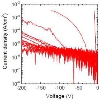
Fig. 5. Reverse J-V Charateristics of Ga2O3 epitaxial layer 그림 5. 성장된 Ga2O3 에피층의 역방향 J-V 특성
Fig. 6. Foward J-V Charateristics of Ga2O3 epitaxial layer 그림 6. 성장된 Ga2O3 에피층의 순방향 J-V 특성
그림 5와 6은 역방향 및 순방향 전류밀도-전압 특성을 보여주고 있다. 그림 5에서 보는 바와 같이 극히 일부 측정위치에서 약간의 누설전류가 있기 하지만, 전체적으로 200V까지는 전류가 흐르 지 않음을 보이고 있으며, 그림 6에서의 순방향 특성에서는 온 저항이 2.9-7.7mΩ·cm2으로 극히 낮은 값을 나타내고 있어, 전력소자로의 응용이 충분하다는 것을 볼 수 있다.
Ⅲ 결론
본 논문에서는 최근 전력반도체 산업에서 활 용되어지는 와이드밴드갭 반도체 중에 하나인 Ga2O3를 이용한 에피웨이퍼 성장에 관련되어 서술 하였다. GaN 성장시 활용되어지는 HVPE법을 이용하여 Sn이 도핑된 Ga2O3 기판웨이퍼에 평균 5.3㎛ 두께로 성장시켰다. 일반적으로 화합물반도 체의 에피 두께가 5㎛일 경우 SiC의 경우 600V 전력반도체 소자를 제작할 수 있으며, Ga2O3 에 피웨이퍼의 경우에는 1000V이상의 전력소자를 제작할 수 있다. 성장된 에피웨이퍼의 J-V 측정 결과 2.9-7.7mΩ·cm2의 온저항을 얻을 수 있었으 며, 역방향의 경우 상당히 높은 전압에서도 누설 전류가 거의 없음을 알 수 있었다.
References
[1] T. Onuma, S. Saito, K. Sasaki, T. Masui, T. Yamaguchi, T. Honda, and M. Higashiwaki,
“Valence band ordering in β-Ga2O3 studied by polarized transmittance and reflectance spectroscopy,” Jpn. J. Appl. Phys., vol. 54, no. 11, p. 112601, 2015.DOI:10.7567/JJAP.54.112601
[2] K. Sasaki, M. Higashiwaki, A. Kuramata, T.
Masui, and S. Yamakoshi, “Ga2O3 Schottky barrier diodes fabricated by using single-crystal β–Ga2O3 (010) substrates,” IEEE Electron Device Lett., vol. 34, no. 4, pp. 493–495, 2013.
DOI:10.1109/LED.2013.2244057
[3] M. Higashiwaki, K. Sasaki, K. Goto, K.
Nomura, Q. T. Thieu, R. Togashi, H. Murakami, Y. Kumagai, B. Monemar, A. Koukitu, A. Kuramata, and S. Yamakoshi, “Ga2O3 Schottky barrier diodes with n−-Ga2O3 drift layers grown by HVPE,” in Proc. 73rd IEEE Device Res. Conf., pp. 29–30, 2015. DOI:10.1109/DRC.2015.7175536
[4] M. Higashiwaki, K. Sasaki, A. Kuramata, T.
Masui, and S. Yamakoshi, “Gallium oxide (Ga2O3) metal-semiconductor field-effect transistors on single-crystal β-Ga2O3 (010) substrates,” Appl.
P hys. Lett., vol. 100, no. 1, p. 013504, 2012.
DOI:10.1063/1.3674287
[5] K. Sasaki, M. Higashiwaki, A. Kuramata, T.
Masui, and S. Yamakoshi, “Si-ion implantation doping in β-Ga2O3 and its application to fabrication of low-resistance ohmic contacts,”
Appl. Phys. Exp., vol. 6, no. 8, p. 086502, 2013.DOI:10.7567/APEX.6.086502
[6] M. Higashiwaki, K. Sasaki, T. Kamimura, M.
H. Wong, D. Krishnamurthy, A. Kuramata, T.
Masui, and S. Yamakoshi, “Depletion-mode Ga2O3 MOS field-effect transistors on β-Ga2O3 (010) substrates and temperature dependence of their device characteristics,” Appl. Phys. Lett., vol. 103, no. 12, p. 123511, 2013.
BIOGRAPHY
Ey-Goo Kang(Member)
1993 : BS degree in Electrical Engineering, Korea University 1995 : MS degree in Electrical Engineering, Korea University 2002 : Ph. D degree in Electrical Engineering, Korea University 2003∼2018 : Professor, Far East University.
Faculty is Power Devices and ICs.