• 검색 결과가 없습니다.

Automated Wafer Separation from the Stacked Array of Solar Cell Silicon Wafers Using Continuous Water Jet

N/A
N/A
Protected

Academic year: 2021

Share "Automated Wafer Separation from the Stacked Array of Solar Cell Silicon Wafers Using Continuous Water Jet"

Copied!
5
0
0

로드 중.... (전체 텍스트 보기)

전체 글

(1)

Automated Wafer Separation from the Stacked Array of Solar Cell Silicon Wafers Using Continuous Water Jet

Kyoungjin Kim, Dongjoo Kim and Ho Sang Kwak

School of Mechanical Engineering, Kumoh National Institute of Technology

ABSTRACT

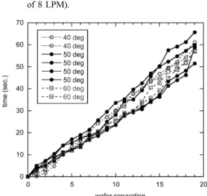
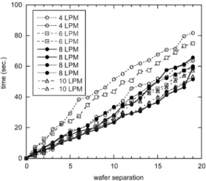
In response to the industrial needs for automated handling of very thin solar cell wafers, this paper presents the design concept for the individual wafer separation from the stacked wafers by utilizing continuous water jet. The experimental apparatus for automated wafer separation was constructed and it includes the water jet system and the microprocessor controlled wafer stack advancing system. Through a series of tests, the performance of the proposed design is quantified into the success rate of single wafer separation and the rapidity of processing wafer stack. Also, the inclination angle of wafer equipped cartridge and the water jet flowrate are found to be important parameters to be considered for process optimization. The proposed design shows the concept for fast and efficient processing of wafer separation and can be implemented in the automated manufacturing of silicon based solar cell wafers.

Key Words : Silicon Wafer, Solar Cell, Wafer Separation, Water Jet

1. Introduction

Ever since the development in 1950s, the solar cells have become the most viable alternatives for clean and renewable energy generation in the form of electricity to the conventional fossil fuel based energy sources. There are a few different types of the solar cells under intensive activities of research and development. However, despite the numerous attempts at improving solar cells by using new materials and technologies, monocrystalline or polycrystalline silicon wafer based solar cells still dominate the current photovoltaic market and these first generation solar cells contribute approximately 90 percent of world market [1].

Currently, one of the major challenges that the photovoltaic industry is facing is that the silicon based solar cells require high purity defect free silicon and the material cost of silicon is too high. In fact, more than half of the module cost is due to the cost of processed silicon wafers [2], which is actually

incurred only because of mechanical reasons, since most of the solar absorption occurs on the solar cell surface within a few tens of microns in depth [3].

Therefore, in order to reduce the material cost, the photovoltaic industry has been making serious efforts to continually reduce the thickness of the wafers for solar cell manufacturing, as shown in Fig. 1 [4]. The solar cell wafer thickness was approximately 300 µm in 2003 and presently it reached 200 µm at the commercialization stage. Some research has been carried out to reduce the wafer thickness down to 100 µm. According to the reports by Q-Cells, the German

E-mail : [email protected]

Fig. 1. Timeline for the decrease in the solar cell wafer

thickness [4].

(2)

solar cell manufacturer, 70 µm decrease in wafer thickness has lead to approximately 10 to 15 percent cost reduction [4].

In manufacturing of silicon wafers for solar cells, one of the technical difficulties arises from the adhesion between the adjacent wafers immediately after the wire sawing of silicon ingot and it is extraordinarily difficult to separate the each wafer from the stacked wafer arrays in a timely manner.

Also, it becomes more and more difficult by the industrial trend of making thinner wafers. Thus, the process of wafer separation can be the bottleneck in the solar cell wafer production and the efficient method for handling this process should be developed to increase the productivity of the solar cell manufacturing. This paper presents the automated separation of the individual wafer from the stacked wafer array by using continuous water jet.

2. Apparatus and Experiments

Since the silicon based solar cells are basically the semiconductor devices, the manufacture of the solar cell wafers is fairly similar to that of the silicon wafers for semiconductor devices, both of which include the preparation and the slicing of silicon ingot to make silicon wafers. After the polycrystalline silicon ingot is block casted, ingot is sliced by wire sawing into very thin wafers, and then the individual wafer gets cleaned and dried before being shipped to the cell processing. The apparatus and the methodology developed in the present study addresses the solar cell wafer separation process that lies between the wire sawing of silicon ingot and the surface cleaning of wafers.

Adhesion between two flat and highly polished solid surfaces can be either dry adhesion due to the contact forces such as the van der Waals forces or wet adhesion due to the capillary action of liquid film [5].

In the present case, the mechanism of wafer to wafer adhesion is expected to be dominated by the wet adhesion because of the DI water involvement in the wire sawing and cleaning processes.

In order to overcome the wet adhesion between the square shaped wafers and achieve the wafer separation,

the use of water jet is expected to be effective method. The experimental investigation by Kim et al.

[6] showed the penetration of water underneath the wafer and the mechanism of wafer separation by water jet, although it concerns the separation of circular shaped semiconductor silicon wafers of 1 mm thickness from the porous pad.

Fig. 2 shows the presently developed apparatus for the automated separation of solar cell wafers from the stack of multiple wafers. It is designed to process the wafers with the size of 156 × 156 mm. By driving the step motor, stacked wafers loaded in the cartridge are pushed into the water jet zone via the gear system of rack and pinion. The 32 bit ARM RISC microprocessor equipped controller system (Atmel AT91SAM7S256) is used to control the step motor as illustrated in Fig.

3, and it is programmed to let the linear motion of stacked wafer be discrete with a fine moving interval that corresponds to the half of wafer thickness (100 µm), so the wafer stack stops and waits until the wafer at the front is separated and slipped away by water jet. Note that it takes 1 second for wafer stack to advance 0.1 mm.

Flowrate of water jet is controlled and measured by a flowmeter of float displacement type (Unicell LF301). Water jet could be also discrete but it is set to be continuous for the simplicity of design. In the tests, the aluminum plates of identical dimensions and thickness are used instead of silicon wafers, since the

Fig. 2. Schematic of the automated wafer separation apparatus

using continuous water jet.

(3)

actual wafers are too expensive.

A series of tests were carried out to evaluate the effectiveness of the proposed design and one test is defined as the processing of a wafer stack of at least 20 wafers loaded in the cartridge of the apparatus. In every test, the time and the number of wafers separated are measured and recorded each time the wafer separation occurs during the processing of a wafer stack.

3. Results and Discussion

In this experimental study, the presently proposed design for the automated wafer separation has been tested for two different aspects of the effectiveness.

First would be the success rate of single wafer separation, which is calculated as the percentage of the number of single wafer separation to the total number of wafer separation in each test. Secondly, the time interval between the subsequent wafer separations is measured in order to evaluate the rapidity of the wafer handling.

The effects of two major parameters, the inclination angle of the cartridge and the flowrate of water jet, are investigated. Each test lasts while the wafer separation occurs 20 times from the start. However, the first wafer separation is not counted and the time is measured from the point when first wafer separation occurs in order to exclude the initiation effects, if there are any. Therefore, the experimental results from each test will have 19 events of wafer

separation.

Figs. 4 and 5 present the effects of the inclination angle of the cartridge on the performance of wafer separation by the proposed design. The inclination angles of 40, 50, and 60 degrees are tried and each case is tested multiple times at the water jet flowrate of 8 LPM. Fig. 4 illustrates the numbers of wafer separated in each test at three different inclination angles. In this figure, number 1 in the small boxes represents the successful single wafer separation, while numbers 2 or more implies the multiple wafer separation which is not desirable for the purpose of this study.

Fig. 3. Experimental setup for the automated wafer separation.

Fig. 4. The effect of the inclination angle of cartridge on the number of separated wafer (water jet flowrate of 8 LPM).

Fig. 5. The effect of the inclination angle of cartridge on

the accumulated time of wafer separation (water

jet flowrate of 8 LPM).

(4)

While we find that the occurrence rate of single wafer separation is quite sensitive to the inclination angle of the wafer loaded cartridge, the case of 50 degrees is most successful in single wafer separation and the success rate is found to be 76.3 percent. In contrast, the inclination angle does not affect the rapidity of wafer separation very much, as shown in Fig. 5. In all the cases of different inclination angle, the accumulated time after 19 wafer separations is found to be similar and the average time between wafer separations is approximately 3 seconds, as

listed in Table 1.

The effects of the water jet flowrate, which is also interpreted as the water jet intensity, on the performance of wafer separation are shown in Figs. 6 and 7. The flowrates of 4 to 10 LPM are tried at the fixed inclination angle of 50 degrees. At this time, the increase of water jet flowrate does not improve the success rate of single wafer separation significantly, as shown in Fig. 6. Table 2 lists the success rate of single wafer separation and shows approximately 10 percent of improvement when the flowrate increases from 4 to 10 LPM. However, the increase of the water jet flowrate improves the rapidity of the wafer separation by shortening the processing time. Fig. 7 and the compiled data in Table 2 show this trend. At the flowrate of 4 LPM, the average time interval for wafer separation is close to 4 seconds and it is improved to approximately 3 seconds at the flowrate of 8 LPM. A further increase of flowrate may improve the rapidity of wafer separation moderately, but the increase of success rate becomes smaller, as found in the case of 10 LPM. Also, the possible damaging of fragile silicon wafers should be considered if the water jet intensity becomes too high.

Fig. 6. The effect of the water jet flowrate on the number of separated wafer (inclination angle of 50

o

).

Fig. 7. The effect of the water jet flowrate on the accumulated time of wafer separation (inclination angle of 50

o

).

Table 1. Averaged experimental results from the testing of the inclination angle of cartridge (water jet flowrate of 8 LPM).

inclination angle of cartridge (deg.)

average time of wafer separation

(seconds)

success rate of single wafer separation (%)

40 3.01 57.9

50 3.11 76.3

60 3.16 34.2

Table 2. Averaged experimental results from the testing of the water jet flowrate (inclination angle of 50

o

).

flowrate of water jet

(LPM)

average time of wafer separation

(seconds)

success rate of single wafer separation (%)

4 3.83 63.2

6 3.52 65.8

8 3.11 76.3

10 2.91 71.1

(5)

4. Conclusions

This research proposes the apparatus design that processes the individual wafer separation from the stack of adhered solar cell wafers. The automated wafer separation is realized by using the continuous water jet on the linearly advancing wafer stack.

The effectiveness of the proposed design is tested by investigating the effects of the inclination angle of cartridge and the water jet flowrate. As a result, the inclination angle is found to be critical to success rate of single wafer separation, while the water jet flowrate improves the rapidity of wafer separation processing. Although the present design requires a further refinement for making more perfect operations, this study shows the feasible concept for efficient and fast processing of wafer separation which can be readily implemented in the automated manufacturing of very thin solar cell wafers.

Acknowledgements

This study is the results of the “Human Resource Development Center for Economic Region Leading Industry” Project, which is supported by the Ministry of Education, Science, & Technology (MEST) and

the National Research Foundation of Korea (NRF).

References

1. Burtescu, S., Parvulescu, C., Babarada, F., and Manea, E., “The Low Cost Multicrystalline Silicon Solar Cells,” Materials Science and Engineering B, Vol. 165, pp. 190-193, 2009.

2. Goetzberger, A., Luther, J., and Willeke, G., “Solar Cells: Past, Present, Future,” Solar Energy Materials

& Solar Cells, Vol. 74, pp. 1-11, 2002.

3. Bagnall, D. M. and Boreland, M., “Photovoltaic Tech- nologies,” Energy Policy, Vol. 36, pp. 4390-4396, 2008.

4. Brand, M., “Solar Cells from Q-Cells,” http://www.q- cells.com, 2008.

5. Legtenberg, R., Tilmans, H. A. C., Elders, J., and Elwenspoek, M., “Stiction of Surface Micromachined Structures After Rinsing and Drying: Model and Investigation of Adhesion Mechanisms,” Sensors and Actuators A, Vol. 43, pp. 230-238, 1994.

6. Kim, K., Kwak, H. S., and Park, K. S., “An Exper- imental Study on Wafer Demounting by Water Jet in a Waxless Silicon Wafer Mounting System,” Journal of the Semiconductor & Display Equipment Technol- ogy, Vol. 8, pp. 31-35, 2009.

접수일: 2010년 5월 14일, 심사일: 2010년 5월 26일

게재확정일: 2010년 5월 31일

수치

Fig. 2 shows the presently developed apparatus for the automated separation of solar cell wafers from the stack of multiple wafers
Fig. 5. The effect of the inclination angle of cartridge on the accumulated time of wafer separation (water jet flowrate of 8 LPM).
Table 2. Averaged experimental results from the testing of the water jet flowrate (inclination angle of 50 o ).

참조

관련 문서

Therefore, in this paper, the solar array of HST is modeled as a simple model with beams and membranes, and the phenomenon of thermal induced vibration is verified and

The pulses generate an electrochemical reaction, inducing nanoscale silicon oxide deposits on the wafer surface.. This research focused on variations in

In addition, using the properties of water shown in diverse shapes, Ki Hyung-do's recognition on the reality and future consciousness from regression of

Protecting the aquatic ecosystem in the water body Recover water and resources from wastewater and. produce renewable energy using wastewater constituents.. • So, the goal

Green (University of New South Wales), and Reuben Collins (Colorado School of Mines) MRS Bulletin (2008)... World

그 결과 Silicon의 반도체 물성으로 광대역 RF 설계에 많은 어려움이 있는 Silicon Wafer 중에 Low Resistivity Silicon Wafer와 High Resistivity Silicon

The materials machined included not only brittle materials (e.g., silicon wafers) but also flexible materials (e.g., pulse electrochemical polished

Chang Je Park, Kwoen Ho Kang, Sang Ho Na, Young Hee Kim, Ho Jin Ryu, Geun Il Park, and Kee Chan Song (KAERI). Geun-Suk Choi and