Hot Wall Epitaxy (HWE)법에 의한 ZnIn 2 Se 4 단결정 후막 성장과 열처리 효과
홍명석·홍광준* †
Growth and effect of thermal annealing for ZnIn 2 Se 4 single crystalline thick film by hot wall epitaxy
Myungseuk Hong and Kwangjoon Hong* † Abstract
Single crystalline ZnIn
2Se
4layers were grown on thoroughly etched semi-insulating GaAs (100) substrate at 400
oC with hot wall epitaxy (HWE) system by evaporating ZnIn
2Se
4source at 630
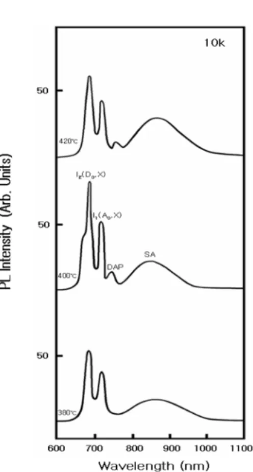
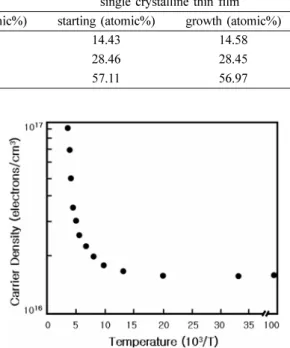
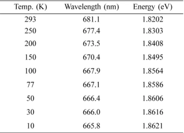
oC. The crystalline structure of the single crystalline thick films was investigated by the photoluminescence (PL) and Double crystalline X-ray rocking curve (DCRC). The carrier density and mobility of ZnIn
2Se
4single crystalline thick films measured from Hall effect by van der Pauw method are 9.41 × 10
16cm
−3and 292 cm
2/V · s at 293 K, respectively. The temperature dependence of the energy band gap of the ZnIn
2Se
4obtained from the absorption spectra was well described by the Varshni ’ s relation, E
g(T)=1.8622 eV − (5.23 × 10
−4eV/K)T
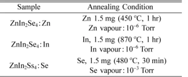
2/(T +775.5 K). After the as-grown ZnIn
2Se
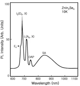
4single crystalline thick films was annealed in Zn-, Se-, and In-atmospheres, the origin of point defects of ZnIn
2Se
4single crystalline thick films has been investigated by the photoluminescence (PL) at 10 K. The native defects of V
Zn, V
Se, Zn
int, and Se
intobtained by PL measurements were classified as a donors or acceptors type. And we concluded that the heat-treatment in the Se-atmosphere converted ZnIn
2Se
4single crystalline thick films to an optical p-type. Also, we confirmed that In in ZnIn
2Se
4/GaAs did not form the native defects because In in ZnIn
2Se
4single crystalline thick films existed in the form of stable bonds.
Key Words : point defect, hot wall epitaxy, single crystalline thick film, thermal annealing, photoluminescence
1. 서 론
ZnIn 2 Se 4 는 I-III-VI 2 족 화합물 반도체로서 상온에서 에너지 띠간격이 1.82 eV 인 직접 천이형 반도체 [1-3] 이 어서 태양전지 [4] , 광전 메모리 소자 [5] , 광전도 소자 [6] , LED(light emitting diode) [7] 등에 응용성이 기대되고
있어 양질의 결정성장과 물성연구가 활발히 진행되고 있다 . ZnIn 2 Se 4 의 성장 방법은 Bridgman-Stockbarger technique [1] , zone levelling [2] , iodine vapour trans- port [4] , liquid encapsulated czochralski(LEC) 법 [5] , 진공 증 착법 [6] , e-beam 증착법 [7] , Hot Wall Epitaxy (HWE) [8] 등
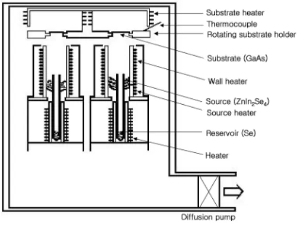
이 있다 . HWE 방법은 증발원을 직접 가열하여 기체상
태로 기판에 도달하고 응집되어 막이 성장되도록 하는 방법인데 열역학적 평형상태에 가까운 조건하에서 결 정을 성장시키므로 양질의 박막을 만들 수 있고 , 시료 의 손실을 줄일 수 있으므로 대량으로 생산할 수 있다 는 장점이 있다 [9] .
Bridgman-Stockbarger technique [1] , iodine vapour transport [4] 법으로 성장시킨 ZnIn 2 Se 4 단결정의 특성에 관한 연구는 이루어졌으나 , 아직까지 HWE 방법으로
성장시킨 ZnIn 2 Se 4 단결정 후막의 기본 물성 및 열처리 효과에 의한 점 결함의 연구는 이루어지지 않았다 . 본 연구에서는 수평 전기로를 제작하여 6 N 의 Zn, In, Se
시료를 mole 비로 칭량하여 starting element 로 하여 수 평로에서 용융 성장법으로 ZnIn 2 Se 4 다결정을 합성하 였다 . 합성된 다결정은 XRD(X-ray diffraction) 을 측정
하여 결정구조 및 격자상수를 구하였다 . 그리고 합성된
조선대학교기계공학과
(Department of Mechenical Engineering, Chosun University)
*
조선대학교물리학과(Department of Physics, Chosun University)
†