• 검색 결과가 없습니다.

Fabrication and Challenges of Cu-to-Cu Wafer Bonding

N/A
N/A
Protected

Academic year: 2021

Share "Fabrication and Challenges of Cu-to-Cu Wafer Bonding"

Copied!
5
0
0

로드 중.... (전체 텍스트 보기)

전체 글

(1)

Fabrication and Challenges of Cu-to-Cu Wafer Bonding

Sung-Geun Kang

1

, Jieun Lee

2

, Eun-Sol Kim

2

, Naeun Lim

2

, Soohyung Kim

1

, Sungdong Kim

2

and Sarah Eunkyung Kim

3,†

1

Microsystem Packaging Center, Seoul Technopark, 232 Gongneung-ro, Nowon-gu, Seoul 139-743, Korea

2

Department of Mechanical System Design Engineering, Seoul National University of Science and Technology, 232 Gongneung-ro, Nowon-gu, Seoul 139-743, Korea

3

Graduate School of NID Fusion Technology, Seoul National University of Science and Technology, 232 Gongneung-ro, Nowon-gu, Seoul 139-743, Korea

(Received March 2, 2012: Corrected May 25, 2012: Accepted June 11, 2012)

Abstract: The demand for 3D wafer level integration has been increasing significantly. Although many technical challenges of wafer stacking are still remaining, wafer stacking is a key technology for 3D integration due to a high volume manufacturing, smaller package size, low cost, and no need for known good die. Among several new process techniques Cu-to-Cu wafer bonding is the key process to be optimized for the high density and high performance IC manufacturing.

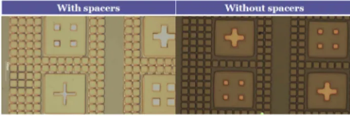
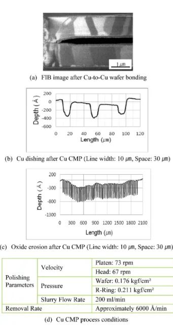
In this study two main challenges for Cu-to-Cu wafer bonding were evaluated: misalignment and bond quality of bonded wafers. It is demonstrated that the misalignment in a bonded wafer was mainly due to a physical movement of spacer removal step and the bond quality was significantly dependent on Cu bump dishing and oxide erosion by Cu CMP.

Keywords: Wafer bonding, Misalignment, Cu bonding, CMP

1. Introduction

3D wafer level integration has been a key technology to microelectronic industries and it is the best for high density and high performance device applications.

1-4)

Although many technical challenges of wafer stacking are still remaining, wafer stacking is a key technology for 3D integration compared to die-to-die, die-to-wafer, or package-to-package due to high volume manufacturing, smaller package size, and no need for known good die. Especially for the high density and high performance, the wafer stacking with a metallic bonding is necessary and Cu-to-Cu wafer bonding is without doubt a key process to be developed. The advantages of Cu as a bonding material are a mainstream CMOS material, low resistivity ( ρ = 1.7 µΩcm), high thermal conductivity (K = 400 W/mK), good resistance to electromigration, and no brittle intermetallic formation.

Many studies for Cu-to-Cu wafer bonding have been explored by many researchers.

5-11)

However, wafer warpage, coefficient of thermal expansion (CTE) mismatch with other layers in a stack, and inherent Cu process issues such as Cu oxidation, bonding surface uniformity, and Cu CMP (chemical mechanical polishing) have not been discussed in detail and it is still remained as the challenges to be resolved for Cu-to-Cu wafer bonding.

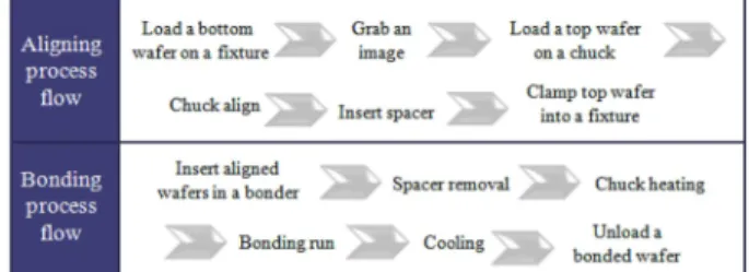
In this study the two main challenges for Cu-to-Cu wafer bonding are evaluated: misalignment and Cu bonding quality. Some report

12)

stated that bond tool and wafer thinning process can introduce a misalignment of bonded wafers. According to our previous study

6)

, it was found that a thin film deposited wafer had a concave-up warpage and a maximum wafer bow became severe as the number of wafer stacks increased. Therefore, wafer warpage might contribute a misalignment of bonded wafer and it might be intensified as the number of wafer stacks increases. Also, the degree of planarization of Cu surface is very important for the best bond quality. Traditionally Cu CMP is not used in electronic packaging field due to a high cost, so other planarization method like a diamond bit cutting has been reported.

8)

However, high density and high performance devices still require Cu CMP.

2. Experimental Procedure

The Cu bump patterned wafers were fabricated on 200 mm Si wafer of approximately 720 µm thick. Ti/Cu barrier and seed layers of 0.15 µm thick were deposited on a Si wafer by sputtering and then approximately 1.2 µm thick Cu was electroplated followed by Cu CMP. The process conditions of Cu CMP are summarized in Fig. 6(d).

Corresponding author

E-mail: [email protected]

(2)

Then a thermo-compression wafer bonding was performed for wafer stacking and the schematic diagram of wafer stack is shown in Fig. 1. A pre-cleaning of Cu bump surface prior to a wafer bonding was done for 1 minute by H

2

SO

4

:DI (1:100) solution in order to remove any surface contamina- tion and native oxide. Two Cu bump patterned wafers were aligned using Suss Microtec aligner (MA8-L) and then Cu-to- Cu wafer bonding was performed at 415

o

C under pressure of 8900mbar for 1 hour using Suss Microtec bonder (SB8e). A forming gas treatment was also performed just before bonding in a bond chamber to clean Cu bump surface. The aligning and bonding process steps are shown step by step in Fig. 2. A bond quality after Cu-to-Cu wafer bonding was investigated by focused ion beam (FIB), scanning electron microscope (SEM) and scanning acoustic microscope (SAM). To evaluate the degree of misalignment, glass-to-Si wafer pairs were used instead of Si wafer-to-Si wafer pairs.

A misalignment after clamping (i.e. before bonding) and after bonding was inspected using a microscope.

3. Results and Discussion

In 3D wafer level packaging, wafer-to-wafer alignment is very important especially for narrow pitched high density devices, because it impacts both device performance and reliability of stacked wafers. The accuracy of alignment can

be dependent on both equipment (aligner and bonder) and process. In this study, glass-to-Si wafer pairs were prepared and inspected after a clamping step to verify any pre- bonding misalignment and after a bonding step to verify any post-bonding misalignment. Also, the misalignment with and without spacers were tested, because a spacer removal step is the only physical movement during a bonding process sequence.

Firstly the misalignment after a clamping step (i.e. after finishing all aligning steps) and after a bonding step is shown in Fig. 3. It is clearly shown that there was almost no misalignment during an aligning process sequence including inserting a spacer and loading aligned two wafers from an aligner to a bonder. But the misalignment after a bonding process sequence was markedly observed about 1 µm in the left side and about 6-7 µm in the right side of bonded wafer.

The left side of bonded wafer had much better alignment accuracy compared to the right side of bonded wafer. The possible cause for this non-symmetric misalignment is supposedly an uneven spacer removal during a bonding Fig. 1. Schematics of Cu-to-Cu wafer bonding.

Fig. 2. Aligning and bonding process flow sequence.

Fig. 3. Misalignment analysis with aspacer: after clamping (i.e.

before bonding) vs. after bonding.

(3)

process, because this step is the only physical movement involved with wafers. It is suggested that the misalignment of bonded wafer was certainly more impacted by a bonding process than an aligning process. Secondly the effect of spacer removal in a bonding process was evaluated and the results are shown in Fig. 4. There was almost no misalignment after bonding without spacers, but the misalignment was clearly observed after bonding with spacers. It seemed that a physical movement of spacer removal from two aligned wafers was the main cause for a misalignment because a wafer has had a great chance to move when three spacers were removed.

To evaluate a bond quality the annealing after bonding was investigated in this study. As shown in Fig. 5(a) three cases were tested such as no annealing, annealing in N

2

, and vaccum annealing. Since Cu oxidize so readily N

2

gas or vaccum was used to reduce oxygen availability during

annealing. In these cases wafer bonding was done with spacers to make forming gas treatment be effective. The SAM images of bonded wafers are shown in Fig. 5(b) and indicated that all three cases were not bonded well since the color image of SAM appeared as an uneven gray color instead of a dark gray or black color which indicates a very weak bond quality. The sample #1 (no annealing) had a clearly unbonded area at the center, and the sample #3 (vaccum annealing) had an unbonded area at the bottom edge of bonded wafer. These unbonded interfaces are shown in the SEM images in Fig. 5(b). These poor bond quality seemed to be nothing to do with annealing conditions nor with a bonding process itself in this study, rather it was likely affected by a bonding layer uniformity. Although it was unable to evaluate the annealing effects on bonding due to the unbonded interface, it showed suggestively how important the planarity of bonding surface was for a good bond quality.

As shown in Fig. 6(a) Cu bump had Cu dishing problem due to Cu CMP process. For example, a structure of 10 µm metal width with 30 µm space had about 400Å Cu dishing and about 500Å oxide erosion as shown in Fig. 6(b) and (c).

Due to Cu bump dishing by Cu CMP, Cu bumps were locally bonded at the edge of each bump causing a very weak bond interface. The previous study by Park et al.

13, 14)

reported that HF and H

2

SO

4

wet treatment of Cu bonding Fig. 4. Misalignment analysis after bonding: with spacers vs.

without spacers.

Fig. 5. Bonding inteface analysis after Cu-to-Cu wafer bonding.

(4)

surface or Ar+H

2

plasma treatment before Cu-to-Cu bonding increased the interfacial adhesion energy and improved Cu- to-Cu bond quality. To improve Cu-to-Cu bonding quality the any oxide removal and contamination-free surface of Cu bonding layer are needed, but the minimization of both Cu bump dishing and oxide erosion is more important and essential to have a reliable and manufacturable wafer bonding.

4. Conclusions

In this study both misalignment and bond quality of Cu-to- Cu wafer bonding were investigated. Cu bumps were fabricated on a Si wafer and Cu bump patterned wafers were bonded by a thermo-compression bonding. A wet chemical treatment on Cu surface before bonding was done and a forming gas treatment was also performed prior to a bonding

process. It has been demonstrated that the controlling of Cu dishing and oxide erosion by Cu CMP was significant to improve Cu-to-Cu wafer bonding quality in addition to pre- surface treatments. Any physical movement step in aligning and bonding processes may affect the accuracy of alignment significantly.

Acknowledgments

This project is conducted through the Practical Application Project of Advanced Microsystems Packaging Program of Seoul Technopark, funded by the Ministry of Knowledge Economy.

References

1. R. S. List, C. Webb and S. E. Kim, “3D Wafer Stacking Tech- nology”, Proc. 19th Adv. Metallization Conference (AMC), 29 (2002).

2. P. Morrow, M. Kobrinsky, M. Harmes, C. Park, S.

Ramanathan, V. Ramachandrarao, H. Mog Park, G. Kloster, S. List and S. Kim, “Wafer-Level 3D Interconnects Via Cu Bonding”, Proc. 21st Adv. Metallization Conference (AMC), San Diego, 125 (2004).

3. J. Balachandran, S. Brebels, G. Carchon, M. Kuijk, W. De Raedt, B. Nauwelaers and E. Beyne, “Wafer-Level Package Interconnect Options”, VLSI, 14(6), 654 (2006).

4. M. Koyanagi, “3D LSI Technology and Wafer-level Stack”, Proc. 2nd International Symposium on

5. Microelectronics and Packaging (ISMP), Seoul, 103, The Korean Microelectronics and Packaging Society, (2003).

6. P. R. Morrow, C. M. Park, S. Ramanathan, M. J. Kobrinsky and M. Harmes, “Three-Dimensional Wafer Stacking Via Cu–

Cu Bonding Integrated With 65-nm Strained-Si/Low- k CMOS Technology”, IEEE Electron Device Letters, 27(5), 335 (2006).

7. Y. Kim, S-K Kang, S. D. Kim and S. E. Kim, “Wafer warpage analysis of stacked wafers for 3D integration”, Microelec- tronic Engineering, 89, 46 (2012).

8. Y. Kim, S. K. Kang and E. K. Kim, “Study of Thinned Si Wafer Warpage in 3D Stacked Wafers”, Microelectronics Reliability, 50, 1988 (2010).

9. W. Ruythooren, A. Beltran and R. Labie, “Cu-Cu Bonding Alternative to Solder based Micro-Bumping”, Proc. 9

th

Elec- tronics Packaging Technology Conference(EPTC), Singapore, 315, IEEE (2007).

10. L. Peng, H. Y. Li, D. F. Lim, G. Q. Lo, D. L. Kwong and C.

S. Tan, “Fabrication and characterization of bump-less Cu-Cu bonding by wafer-on-wafer stacking for 3D IC", Proc. 12

th

Electronics Packaging Technology Conference(EPTC), Sin- gapore, 787, IEEE (2010).

11. C. S. Tan and R. Reif, “Multi-layer silicon layer stacking based on copper wafer bonding”, Electrochemical and solid- state letters, 8(6), 147 (2005).

12. Y-S Tang, Y-J Chang and K-N Chen, “Wafer-level Cu–Cu bonding technology”, Microelectronics Reliability, 52(2), 312 (2012).

Fig. 6. Cu bump dishing and oxide erosion after Cu CMP.

(5)

13. H. W. Zeij and P.M. Sarro, “Alignment and Overlay Charac- terization for 3D Integration and Advanced Packaging”, Proc.

11

th

Electronics Packaging Technology Conference (EPTC), 447, IEEE (2009).

14. J-W Kim, M-H Jeong, E-J Jang and Y-B Park, “Effect of HF/

H2SO4 Pretreatment on Interfacial Adhesion Energy of Cu-

Cu Direct Bonds”, Microelectronic Engineering, 89, 42 (2012).

15. J-W Kim, K-S Kim, H-J Lee, H-Y Kim, Y-B Park and S. M.

Hyun, “Characterization and observation of Cu-Cu Thermo- Compression Bonding using 4-point bending test system”, J.

Microelectron. Packag. Soc., 18(4), 11 (2011).

수치

Fig. 2. Aligning and bonding process flow sequence.
Fig. 5. Bonding inteface analysis after Cu-to-Cu wafer bonding.
Fig. 6. Cu bump dishing and oxide erosion after Cu CMP.

참조

관련 문서

Resistance, Resistivity and Electric conductivity of OFHC Cu, 3DiGn-Cu composite, 3D-Graphene network, Cu powder.. Ratio of resistivity

In addition, this study confirmed the superiority of the thermomechanical reliability of drilled Cu pillar bump (DCPB) through a hysteresis loop, which showed the

Figure 4.15 Measured proportional constant A as a function of Cu content in Al-Si-Cu ternary alloys cast with

CMP process is effectively used to flat dielectric layer such as IMD, ILD, PMD and metal layer such as W, Al, Cu in order to perform multi layer

Consequently, Zr-Cu binary alloys have the potential to be used as biomaterials with nullifying magnetic properties for magnetic resonance imaging diagnosis and

 KAERI tested FSW between 10 mm thick CSC Cu coating and normal cu plate to get a sealing method of a disposal canister.  Before the FSW test, Bead-On test was done on the

W., "The Temperature Dependence of the Diffusion Bonding Between Tungsten Carbides for Micro WC-PCD Tool Fabrication" Journal of the Korean Society

Bonding type: covalent, ionic, metallic, van der waals, hydrogen bond Glass has one of those bonding. Glass has one of