*정회원, 한남대학교 정보통신공학과
접수일자: 2016년 10월 18일, 수정완료 : 2016년 11월 18일 게재확정일자 : 2016년 12월 9일
Received: 18 October, 2016 / Revised: 18 November, 2016 / Accepted: 9 December, 2016
*Corresponding Author: [email protected]
Dept. of Information and Communication Engineering, Hannam University, Korea
https://doi.org/10.7236/JIIBC.2016.16.6.231
JIIBC 2016-6-30
스위치드 본드와이어 인덕터를 이용한 다중대역 CMOS 전압제어발진기 설계
Design of a Multiband CMOS VCO using Switched Bondwire Inductor
류성한
*Seonghan Ryu
*요 약 본 논문에서는 스위치드 본드와이어 인덕터 뱅크를 사용하여, 넓은 주파수 튜닝범위를 갖는 다중대역 저잡음 CMOS 전압제어발진기가 제안되었다. 본드와이어 인덕터와 CMOS 스위치의 결합으로 주파수 튜닝범위는 증가하고, 위상잡음은 개선되었다. 제안된 다중대역 CMOS 전압제어발진기는 2.3GHz부터 6.3GHz까지의 주파수에 대해 동작하 며, 위상잡음은 1MHz 오프셋 주파수에 대해, 각각 -136dBc/Hz와 -122dBc/Hz를 나타내었다. 스위치드 본드와이어 인 덕터 뱅크는 각 주파수 대역에서 높은 Quality factor(Q)를 나타내어, 위상잡음과 전력소모량 사이의 trade-off를 더욱 원활하게 해 준다. 제안된 전압제어발진기는 TSMC 0.18um CMOS공정을 사용하여 설계되었고, 7.2mW의 전력을 사 용하며, 6GHz 발진주파수에 대해 1MHz 오프셋 주파수에서 -189.3dBC/Hz의 성능지수(FOM)를 나타내었다.
Abstract
This paper presents a multiband low phase noise CMOS VCO with wide frequency tunability using switched bondwire inductor bank. The combination of bondwire inductor and CMOS switch transistor enhances frequency tunability and improves phase noise characteristics. The proposed multiband VCO operates from 2.3GHz to 6.3GHz with phase noise of -136dBc/Hz and -122dBc/Hz at 1 MHz offset frequency, respectively. Switched bondwire inductor bank shows high quality factor(Q) at each frequency band, which allows better tradeoff between phase noise and power consumption. The proposed VCO is designed in TSMC 0.18um CMOS process and consumes 7.2 mW power resulting in figure of merit(FOM) of -189.3dBc/Hz at 1 MHz offset from 6GHz carrier frequency.Key Words :
CMOS VCO, Inductor bank, Wide tuning range, Low phase noiseⅠ. Introduction
Among the efforts for the single chip radio integration, the low phase noise VCO implementation gets a lot of attentions[1],[2]. The phase noise of the VCO is one of the most critical parameters for the information transfer. A major challenge in the wireless
industry these days is the establishment of low cost communication terminals, which is highly integrated and can support multiband and multi- standards.
Multiband radio using multiple transceivers can satisfy
these demands, however the complexity and chip area
should be increased. Though design research for RF
building blocks with wide frequency operability has
been progressed, single low phase noise multiband CMOS VCO design is still remain as challenging work[3],[4]. The multiband VCO with wide frequency tunability needs large capacitor banks and varactor diodes, large capacitor banks results area occupation issue and high VCO gain of varactor results phase noise degradation issue. Though these problems can be solved by using highly integrated MIM capacitors occupying less area and by allowing higher power consumption for phase noise characteristics, special passive component such as high-C-MIM and high power consumption is not desirable with continuous CMOS downscaling trend.
This paper describes design of a low phase noise CMOS VCO with very wide frequency tunability using switched bondwire inductor bank. With a 1.2V power supply, this VCO consumes a 6mA bias current at VCO core and shows frequency tunability from 2.3 to 6.3GHz with low phase noise characteristics.
Ⅱ. Bondwire Inductor Issues for VCO
Multiband multi-standard transceiver requires the local oscillator(LO) block with very wide tuning range and low phase noise, therefore simple LO block structure based on only divide-by-two prescaler is favored these days, since side effects of other structures such as self-mixing, DC-offset and frequency pushing or pulling can be minimized. In addition, this simple LO chain structure is the optimum solution to minimize the cost in terms of system complexity, power consumption and area in comparison with other solutions such as a quadrature VCO(QVCO) and a polyphase filter
[5]. For this simple LO structure, VCO core itself should have very wide tuning range. A usual way to achieve a wide tuning range is adopting a switched capacitor bank in a VCO resonator for coarse tuning and a large varactor with high VCO gain, K
vco, for fine tuning. However, a smaller varactor with low K
vcoenables low phase
noise and switched capacitor bank is more suitable for small frequency changes
[6]. Therefore VCO design using inductor switching is a potent candidate solution for wide frequency tunability. The switched inductor bank is generally composed of planar spiral inductors and MOS switches
[7].Considering the size and Quality(Q) factor of the on-chip spiral inductor, single-turn inductor of about 1nH is suitable for several GHz operation. A custom designed single turn inductor can have Q above 15. However, relatively large inductor size, out-diameter larger than 400µm, is usually required. Switched inductor bank with these inductors is not desirable due to area issue. In addition, the Q factor of the custom inductor is still not enough for the stringent phase noise specification. The proper sized planar spiral inductor of conventional CMOS process provides Q of about 10. Therefore, VCO phase noise characteristics may be degraded by switched inductor bank with conventional low Q spiral inductor.
In addition, MOS switch parasitics such as on resistance, R
onmay also worsen the phase noise characteristics.
To resolve this problem, bondwire inductor is proposed in this work. Bondwire inductor shows good quality factor above 25 in the frequency range of interest, from 2 to 6GHz. The inductance of bondwire structure is linearly increased with the bondwire length and can be modified with changing the distance between two bondpads and bondwire height. Figure 1 shows a bondwire inductor VCO with low phase noise characteristics, which has been recently reported
[4]. This VCO exhibits good phase noise performance exceeding the most stringent GSM/EDGE specification while simultaneously achieving enough tuning range.
Though the inductance variation of the bondwire
inductor can be higher than that of on-chip spiral
inductor, more than 20% of the inductance value can
be tuned even after chip fabrication by inserting
dummy tuning pads in circuit layout and changing
bondwire length or height.
Fig. 1. Microphotograph of the bondwire inductor VCO 그림 1. 본드와이어 인덕터 전압제어발진기 사진
Ⅲ. VCO Design
The proposed VCO adopts a switched bondwire inductor bank, which is composed of three bondwire inductors with different length. Figure 2 and figure 3 shows simulated value of the inductance and Q factor for each bondwire inductor. For the characterization of bondwire inductors, an electromagnetic(EM) simulation tool, HFSS is used. In these figures, L_long, L_mid and L_short exhibit bondwire inductor simulation results for length of 700, 525 and 350um respectively.
As depicted in figure. 3, the frequency for maximum Q factor can be varied with bondwire inductance switching, which can improve VCO phase noise characteristics at each frequency band. Figure 4 shows the simulated inductance and Q factor results for shunt connected all three bondwire inductors. Coupling inductances between bondwires are also included in simulation.
Fig. 2. Simulated inductance of switched bondwire inductor
그림 2. 스위치드 본드와이어 인덕터의 인덕턴스 시뮬레이션
Fig. 3. Simulated Q factor of switched bondwire inductor
그림 3. 스위치드 본드와이어 인덕터의 Q 펙터 시뮬레이션
Fig. 4. Simulated Q factor and inductance for shunt connected all three bondwire inductors
그림 4. 병렬 연결된 전체 본드와이어 인덕터의 Q 펙터와 인 덕턴스 시뮬레이션
Fig. 5. VCO structure with switched bondwire inductors
그림 5. 스위치드 본드와이어 인덕터 적용 VCO 구조
The proposed VCO structure is shown in figure 5.
An accumulation-type MOS varactor is used for fine tuning and a switched bondwire inductor bank is used for wide frequency tunability.
As depicted in figure 5, mid and short length bondwire inductors are shunt-connected to long bondwire inductor. The switched inductor bank has lowest total inductance value when all MOS switches are on state, and when all MOS switches are off, mid and short length bondwire inductors have high impedance and are disconnected from the VCO, thus the highest inductance value can be achieved. Though bondwire inductors are connected through MOS switches at on state, the Q factor degradation from MOS R
onresistance can be mitigated due to shunt connection with long bondwire inductor which is directly connected to VCO oscillation node without MOS switch. For the VCO design topology, the NMOS-only type is adopted as depicted in figure 5.
The well-known phase noise model for an oscillator is Leeson’s proportionality
[8].
∆∝
∙
∙
∙
(1)
Where the phase noise is given by kT/C noise that is shaped in frequency domain by LC tank and normalized to the power in the tank. This expression reveals the dependency of the phase noise upon the signal amplitude V
o. For the NMOS-only topology, VCO enables higher voltage swing above VDD limit, thus the phase noise can be improved as the bias current increases. Considering various lossy components of the real circuits on silicon substrate, enough phase noise margin is necessary to satisfy stringent phase noise constraints of various mobile communication standards. For minimizing power consumption, the VCO bias current is varied between each frequency band by controlling the 3-bit binary weighted bias resistors. This programmability allows the trade-off between power consumption and phase noise, which is necessary for the multiband and
multi-standard VCOs. Considering these multiband low phase noise VCO design issues, the proposed VCO is designed in 0.18 mm CMOS technology.
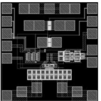
Figure 6 shows the complete layout of the VCO. The chip size is 0.75 × 0.75 mm
2. The layout contains dummy bond pads for inductance modification after chip fabrication.
Fig. 6. Layout of the proposed CMOS VCO 그림 6. 제안된 CMOS 전압제어발진기의 레이아웃
Ⅳ. Simulation Results
The proposed switched bondwire inductor VCO is simulated using S-parameters of bondwire inductors, which is acquired using EM simulation tool, HFSS.
The simulated frequency tuning range of the proposed
VCO is shown in figure 7. The carrier signal
frequency of the VCO is tunable from 2.28 to 2.33GHz
when all MOS switches are at off, and when all MOS
switches are at on state, the carrier is tunable from 6.1
to 6.38GHz. The frequency band between 2.33 and
6.1GHz can be covered by separately controlling each
MOS switch in the inductor bank as depicted in mid
band of figure 7. The full tuning range can also be
covered by utilizing both switched capacitor bank and
switched inductor bank.
Fig. 7. Simulated frequency tuning range of the VCO
그림 7. CMOS 전압제어발진기 VCO 주파수튜닝 시뮬레이션
Fig. 8. Simulated phase noise of the VCO 그림 8. CMOS 전압제어발진기 VCO 위상잡음 시뮬레이션
Fig. 8 shows the simulated phase noise for the VCO, which exhibits a phase noise of -127 and -136dBc/Hz at 400kHz and 1MHz offsets from the 2.3GHz carrier, respectively. For the 6.2 GHz carrier, a phase noise of -113.8 and -122dBc/Hz at 400KHz and 1MHz offsets are attained, respectively. The VCO core operates with 1.2V supply and consumes 6mA. A widely used figure of merit(FOM) for VCO is defined as
[9]
(2)
Here, L{f
offset} is the measured phase noise at offset frequency f
offsetfrom the carrier frequency f
o. P
DCis
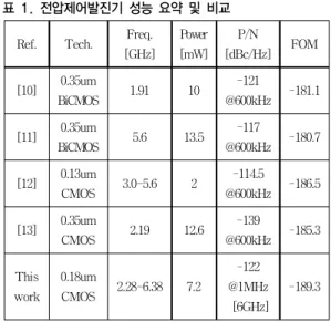
VCO power consumption in mW. The worst simulated FOMs for the VCO is -189.3 dBc/Hz at 6 GHz carrier frequency. Table 1. shows the summary of the simulation results compared to those of other low phase noise VCOs.
Table 1. VCO performance summary and comparisom
표 1. 전압제어발진기 성능 요약 및 비교
Ref. Tech. Freq.[GHz]
Power [mW]
P/N
[dBc/Hz] FOM [10] 0.35um
BiCMOS 1.91 10 -121
@600kHz -181.1 [11] 0.35um
BiCMOS 5.6 13.5 -117
@600kHz -180.7 [12] 0.13um
CMOS 3.0-5.6 2 -114.5
@600kHz -186.5 [13] 0.35um
CMOS 2.19 12.6 -139
@600kHz -185.3
This work
0.18um
CMOS 2.28-6.38 7.2
-122
@1MHz [6GHz]
-189.3
Ⅴ. Conclusion
In this work, a low phase noise, multiband CMOS VCO with wide frequency tunability through bondwire inductor switching has been presented. The proposed VCO is designed with TSMC 0.18 um CMOS process.
An NMOS-only structure and high Q bond wire
inductor are adopted for enough phase noise margin,
wide frequency tunability, and chip area efficiency, and
programmable 3-bit bias resistors are used for a
trade-off between phase noise and power
consumption. The proposed switched bondwire
inductor bank is composed of CMOS switch and
bondwire inductors, which enable very wide frequency
tunability and low phase noise characteristics. The
simulation results show the tuning range from 2.3 to
6.4GHz. The phase noise performance of the VCO is
-122dBc/Hz at 1MHz offset from 6GHz carrier
frequency and the calculated FOM is -189.3dBc/Hz.
These simulation results confirm that a good tradeoff among phase noise, wide tunability and power consumption is achieved from the proposed CMOS VCO with switched bondwire inductor.
References
[1] Jeong-Sig An, Hong-Gil Yoo, “Study on the Phase Noise Improvement of Oscillator using RF Feedback”, Journal of the Institute of Internet, Broadcasting and Communication JIIBC, Vol.4, No.1, pp 51-55, Jan 2004
[2] Jeong-Jin Kang, Wan-sik Kim, Dong-Joon Lee and Edward J Rothwell, “Reconfigurable MMIC VCO Design for Wireless Ubiquitous Communications”, Journal of the Institute of Internet, Broadcasting and Communication JIIBC, Vol.8, No.2, pp 67-73, Feb 2008
[3] S. Ryu, Y. Chung, H. Kim, J. Choi, and B. Kim,
“Phase noise optimization of CMOS VCO through harmonic tuning”, in IEEE Radio Freq. Integr.
Circuits Symp., Long Beach, CA. pp. 403–406, Jun. 2005
DOI: http://dx.doi.org/10.1109/RFIC.2005.1489825 [4] K. Lee, H. Yu, H. Ahn, H. Oh, S. Ryu, D. Keum
and B. Park, “A 0.13-um CMOS Σ-Δ Frequency Synthesizer with an Area Optimizing LPF, Fast AFC Time, and a Wideband VCO for WCDMA/GSM/GPRS/ EDGE Applications”, in IEEE Radio Freq. Integr. Circuits Symp., Atlanta, GA. pp. 299–302, Jun. 2008
DOI: http://dx.doi.org/10.1109/RFIC.2008.4561440 [5] A. Koukab, Y. Lei, M. J. Declercq, “A
GSM-GPRS/UMTS FDD-TDD/WLAN 802.11a-b-g Multi-Standard Carrier Generation System,” IEEE J. Solid-State Circuits, vol. 41, pp. 1513-1521, July. 2006
DOI: http://dx.doi.org/10.1109/JSSC.2006.873928 [6] Z.Li and K.K.O, “A Low-Phase-Noise and
Low-Power Multiband CMOS Voltage-Controlled Oscillator,” IEEE J. Solid-State Circuits, vol. 41, pp. 1296-1302, June. 2005
DOI: http://dx.doi.org/10.1109/JSSC.2005. 848031 [7] S. Yim and K.K.O, “Switched Resonators and
Their Applications in a Dual-Band Monolithic CMOS LC-Tuned VCO,” IEEE Trans. Microw.
Theory Tech., vol. 54, no. 1, pp. 74-81, Jan. 2006 DOI: http://dx.doi.org/10.1109/TMTT.2005.856102 [8] D. B. Leeson, “A Simple Model of Feedback Oscillator Noise Spectrum,” Proceedings of the IEEE, vol. 54, pp. 329–336, 1966
DOI: http://dx.doi.org/10.1109/PROC.1966.4682 [9] A. Wagemans, “A 3.5 mW 2.5 GHz diversity
receiver and a 1.2 mW 3.6 GHz VCO in silicon-on-anything”, IEEE Int. Solid-State Circuits Conf. Tech. Dig., pp. 250-251, Feb. 1998 DOI: http://dx.doi.org/10.1109/ISSCC.1998.672456 [10] D. Ham and A. Hajimiri, “Concepts and methods
in optimization of integrated LC VCOs”, IEEE J.
Solid-State Circuits, vol. 36, pp. 896–909, Jun.
2001
DOI: http://dx.doi.org/10.1109/4.924852
[11] G. De Astis, D. Cordeu, J. Paillot, and L.
Dascalescu, “A 5-GHz fully integrated full pMOS Low-phase-noise LC VCO”, IEEE J. Solid-State Circuits, vol. 40, pp. 2087–2091, Oct. 2005 DOI: http://dx.doi.org/10.1109/JSSC.2005.854601 [12] N. Fong, “Design of wideband CMOS VCO for
multiband wireless LAN applications”, IEEE J.
Solid-State Circuits, vol. 38, pp. 1333–1342, Aug.
2003
DOI: http://dx.doi.org/10.1109/JSSC.2003.814440 [13] P. Adreanj and H. Sjoland, “A 2.2 GHz CMOS
VCO with inductive degeneration noise suppression”, in Proc. IEEE Custom Integrated Circuit Conf., San Diego, CA, pp. 197–200, May.
2001
DOI: http://dx.doi.org/10.1109/CICC.2001.929754
※ This research was supported by Korea Electric Power Corporation through Korea Electrical Engineering & Science Research Institute (grant number : R15XA03-67) and was supported by Basic Science Research Program through the National Research Foundation of Korea(NRF) funded by the Ministry of Education, Science and Technology (No.2011-0014304). This work was also supported by IDEC(EDA Tool, MPW)
저자 소개
류 성 한(정회원)
∙2005년 : 포항공과대학교 전기전자공학 과 박사
∙2005년 ~ 2007년 : 삼성전자 책임연구원
∙2007년 ~ 2008년 : 국방기술품질원 선 임연구원
∙2008년 ~ 현재 : 한남대학교 정보통신 공학과 부교수
<주관심분야 : RF 송수신기 구조 및 CMOS IC설계>