Regular Paper 291 J. Korean Inst. Electr. Electron. Mater. Eng.
Vol. 28, No. 5, pp. 291-294 May 2015
DOI: http://dx.doi.org/10.4313/JKEM.2015.28.5.291 ISSN 1226-7945 (Print), 2288-3258 (Online)
Al Doped ZnO층 적용을 통한 ZnO 박막 트랜지스터의 전기적 특성과 안정성 개선
엄기윤
1
, 정광석2
, 윤호진2
, 김유미2
, 양승동2
, 김진섭2
, 이가원2,a
1 충남대학교 차세대기판학과
2 충남대학교 전자전파정보통신공학과
Improvement of Electrical Performance and Stability in ZnO Channel TFTs with Al Doped ZnO Layer
Ki-yun Eom
1, Kwang-seok Jeong
1, Ho-jin Yun
1, Seung-dong Yang
1, Jin-seop Kin
1, and Ga-won Lee
1,a1 Department of Electronics Engineering, Chungnam University, Daejeon 305-764, Korea
(Received March 20, 2015; Revised April 1, 2015; Accepted April 7, 2015)
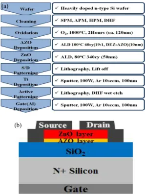
Abstract: Recently, ZnO based oxide TFTs used in the flexible and transparent display devices are widely studied.
To apply to OLED display switching devices, electrical performance and stability are important issues. In this study, to improve these electrical properties, we fabricated TFTs having Al doped Zinc Oxide (AZO) layer inserted between the gate insulator and ZnO layer. The AZO and ZnO layers are deposited by Atomic layer deposition (ALD) method. I-V transfer characteristics and stability of the suggested devices are investigated under the positive gate bias condition while the channel defects are also analyzed by the photoluminescence spectrum. The TFTs with AZO layer show lower threshold voltage (Vth) and superior sub-threshold slop. In the case of Vth shift after positive gate bias stress, the stability is also better than that of ZnO channel TFTs. This improvement is thought to be caused by the reduced defect density in AZO/ZnO stack devices, which can be confirmed by the photoluminescence spectrum analysis results where the defect related deep level emission of AZO is lower than that of ZnO layer.