Nomenclature
CZTSSe : Cu 2 ZnSn(S,Se) 4 V oc : open-circuit voltage, V J sc : short-circuit current, mA/cm 2 FF : fill factor
EQE : External quantum efficiency
Subscript
TFSCs : thin film solar cells RTA : rapid thermal annealing XRD : X-ray diffraction
FE-SEM : field emission scanning electron microscopy
1. 서 론
Cu 2 ZnSn(S,Se) 4 (CZTSSe)는 kesterite 기반의 물질로서 기존 의 박막형 태양전지인 CdTe와 Cu(In,Ga)S 2 (CIGS) 가 갖는 독성 과 희토류 금속 사용이라는 한계를 극복하여 차세대 박막형 태양 전지의 흡수층으로 각광받고 있다. 이러한 CZTSSe 흡수층은 풍 부한 자원과 무독성의 물질을 사용하며 10 4 cm -1 의 높은 흡수계 수와 1.1~1.5eV의 직접천이형 밴드갭의 특성을 보임으로써 저 비용, 고효율의 잠재력을 가진 물질로 평가 되었다 1-3) .
CZTSSe의 합성 방법으로는 evaporation 4) , pulsed laser deposition 5) , electro-deposition 6) , sol-gel 7) , sputtering 8) 등이 있 으며 여러 가지 합성 방법 중 무독성의 고품질 합성 방법인 sputtering 은 초기 katagri 그룹에서 CZTS박막으로 6.77% 효율 을 보고한 바 있다 9) . 또한 최근 IBM에서 hydrazine을 이용한 나 노 합성 방법으로 세계최고 효율인 12.7%을 달성하였다 10) .
그러나 이러한 노력에도 CZTSSe박막 태양전지는 CIGS 의
DOI:https://doi.org/10.21218/CPR.2017.5.1.020 eISSN 2508-125X
Mo 패턴을 이용한 3-D 구조의 Cu
2
ZnSn (Sx
Se1-x
)4
(CZTSSe) 박막형 태양전지 제작조은진
1)
ㆍ강명길1)
ㆍ신형호1)
ㆍ윤재호2)
ㆍ문종하1)
ㆍ김진혁1)
*1)전남대학교 신소재공학부, 광주광역시, 61186
2)한국에너지기술연구원 신재생에너지연구본부, 대전광역시, 61005
3-D Structured Cu 2 ZnSn (S x Se 1-x ) 4 (CZTSSe) Thin Film Solar Cells by Mo Pattern using Photolithography
Eunjin Jo
1)
․ Myeng Gil Gang1)
․ Shin hyeong ho1)
․ Jae Ho Yun2)
․ Jong-ha Moon1)
․ Jin Hyeok Kim1)
*1)
Optoelectronic(s) Convergence Research Center and Department of Materials Science & Engineering, Chonnam National University, 300, Yongbong-Dong,Buk-Gu, 61186, Gwangju, South Korea
2)
Photovoltaic Laboratory, Korea Institute of Energy Research, 152 Gajeong-ro, Yuseong-gu, 61005,Daejeon, South Korea
ABSTRACT: Recently, three-dimensional (3D) light harvesting structures are highly attracted because of their high light harvesting capacity and charge collection efficiencies. In this study, we have fabricated Cu
2ZnSn(S
xSe
1-x)
4based 3D thin film solar cells on PR patterned Molybdenum (Mo) substrates using photolithography technique. Specifically, Mo patterns were deposited on PR patterned Mo substrates by sputtering and the thin Cu-Zn-Sn stacked layer was deposited over this Mo patterns by sputtering technique. The stacked Zn-Sn-Cu precursor thin films were sulfo-selenized to form CZTSSe pattern. Finally, CZTSSe absorbers were coated with thin CdS layer using chemical bath deposition and ZnO window layer was deposited over CZTSSe/CdS using DC sputtering technique. Fabricated 3-D solar cells were characterized by X-ray diffraction (XRD), X-ray fluorescence (XRF) analysis, Field-emission scanning electron microscopy (FE-SEM) to study their structural, compositional and morphological properties, respectively. The 3% efficiency is achieved for this kind of solar cell. Further efforts will be carried out to improve the performance of solar cell through various optimizations.
Key words: 3-D structure, Thin film solar cell, CZTSSe, Deposition of Mo
*Corresponding author: [email protected]
Received February, 11, 2017; Revised February, 26, 2017;
Accepted March, 03, 2017
ⓒ 2017 by Korea Photovoltaic Society
This is an Open Access article distributed under the terms of the Creative Commons Attribution Non-Commercial License (http://creativecommons.org/licenses/by-nc/3.0)
which permits unrestricted non-commercial use, distribution, and reproduction in any medium, provided the original work is properly cited.
20
율이 높아지고 전하 수집 또한 증가하여 태양전지 효율 개선에 잠재력을 가지고 있다 11-13) . 서울대에서 발표한 논문에 따르면 Si 기반의 잘 정렬된 3-D 구조의 태양전지는 평면 태양전지 효 율에 비해 약 2% 증가한 8.1%의 효율을 달성하여 3-D 구조의 태양전지의 효율증대의 가능성을 보였다 13) . 그러나 plasmon을 이용한 복잡한 구조이며 실리콘기반이기 때문에 저비용 고효 율의 한계를 보였으며 이후 현재까지 CZTSSe 기반의 잘 정렬 된 3-D 구조의 태양전지에 관한 보고가 극히 드물다.
따라서 본 연구에서는 sputtering를 이용하여 증착한 평면 CZTSSe 흡수층의 조성비 유지와 동시에 3-D구조를 적용하기 위한 방법으로 후면 전극인 Mo를 패턴화 했다. 이를 이용하여 3-D구조의 흡수층을 가진 태양전지 소자를 제작하였고 그에 따 른 특성을 평가 하였다.
2. 실험방법
2.1 기판준비
2.5×2.5 cm 2 크기의 soda lime glass 기판위에 Mo 박막을 DC sputtering법을 이용하여 1 µm 두께로 제조하였다. 기판 표면 의 불순물을 제거하기 위하여 증류수와 1:3 비율로 희석한 암모 니아 용액에 30초간 세척후 증류수로 린스하였다.
2.2 3-D 구조의 CZTSSe 박막 제조
2.2.1 Photoresist(PR) 패턴 제작
Mo 가 증착된 SLG기판을 아세톤과 메탄올용액에 순서대로 150°C에서 10분간 각각 세척하였다. 기판위에 phoresist 용액 (AZ LoF 2035)을 4500rpm으로 스핀코팅 후 포토리소그래피 를 통하여 지름, 간격, 높이가 각각 5 µm, 1 µm , 3 µm인 PR 패 턴을 제작하였다.
2.2.2 Mo 패턴 제작
PR 패턴된 기판과 Mo층의 접착력을 위해 DC sputtering법 으로 1.5mtorr의 공정압력에서 30분 그리고 30mtorr의 공정압 력에서 25분동안 순서대로 PR패턴 기판위에 증착하였다.
이후 기판의 PR을 제거하기 위해 아세톤에서 1분간 세척하 여 Mo 패턴을 제작하였다.
2.2.3 CZT 금속 전구체 제조
Zn, Sn, Cu의 금속타겟을 사용한 DC sputtering법으로 Mo가
전구체의 Cu-Zn와 Cu-Sn alloy 형성을 위해 Furnace를 이용 하여 300°C에서 1시간동안 열처리를 진행하였다. 황화-셀렌화 공정은 단시간 열처리 공정을 통하여 Rapid thermal annealing (RTA)장비를 이용하여 진행하였다. graphite box 안에 전구체 와 함께 Se과S의 혼합 분말0.2 g (Se : S = 10 : 1) 을 넣고 520°C 에서 10분간 열처리를 하여 CZTSSe 흡수층 박막을 합성하였 고 황화-셀렌화 공정이 끝난후에는 자연 상태에서 냉각 시켰다.
2.3 3-D 구조의 CZTSSe 박막 특성 분석
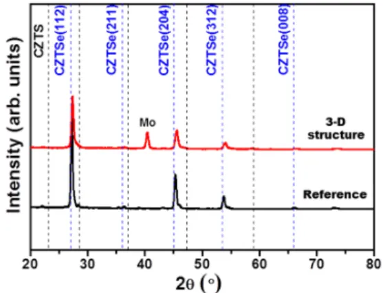
3-D 구조 박막의 미세구조및 표면과 단면의 형태분석을 위하 여 전계 방출형 주사 현미경(Field Emission Scanning Electron Microscopy, FE-SEM, JSCM-6701F, Japan)을 이용하였다. X 선 회절 분석기(X-ray diffraction, XRD, X’pert PRO, Philips, Netherlands), Raman spectroscopy를 이용하여 결정성을 확인 하였다.
2.4 3-D 구조의 CZTSSe 박막의 태양전지 제작 및 효율 측정