2 3
the crystallinity. The optimal growth temperature range was about 460~510oC, and the α-Ga2O3 thin films with the highest crystallinity were obtained at a III/VI ratio of 4. The thickness and surface morphology of the thin films was observed by scanning electron microscopy. The film thickness was 6.938 μm, and the full width at half maximum of the ω-2θ scan rocking curve was as small as 178 arcsec. The optical band gap energy obtained was 5.21 eV, and the films were almost completely transparent in the near-ultraviolet and visible regions. The etch pit density was found to be as low as about 6.0 × 104 cm−2.
Keywords: HVPE, α-Ga2O3, Al2O3, Heteroepitaxy, Single crystal
1. Introduction
Recently, gallium oxide (Ga2O3), an ultra-wide bandgap (UWBG) semiconductor, has been actively studied to replace GaN and SiC.1-4) Owing to the ultra-wide energy bandgap, Ga2O3 can realize high-power devices with higher breakdown voltage and lower energy loss than GaN and SiC.5-8)
Ga2O3 are grown in five phases (α, β, γ, ɛ, and δ) depending on growth parameters such as the growth tem- perature and pressure.9
Among them, the α-phase has a bigger bandgap (5.3 eV) than those of the other phases and is meta-stable at high temperatures (<600oC).10) So far, the heteroepitaxial growth of α-Ga2O3 is possible on sapphire (α-Al2O3) substrates via mist chemical vapor deposition (mist-CVD),11) halide vapor phase epitaxy (HVPE),12,13) and molecular beam epi- taxy (MBE).14)
Growth of α-Ga2O3 via HVPE is type of chemical vapor deposition (CVD) method that has a rapid deposition rate and yields crystals of high purity. HVPE can grow thin films at a lower cost than other methods such as metal organic chemical vapor deposition (MOCVD) and MBE.
Therefore, it is widely used in the III/V semiconductor industry.15)
Previous studies have focused on heteroepitaxial growth on various substrates including sapphire substrates. Since α-Al2O3 have the same corundum structure as α-Ga2O3, Al2O3 is an optimal substrate for heteroepitaxial growth.
Lattice mismatches between α-Ga2O3 and sapphire are about ~4.5% and ~3.3% along the a-axis and c-axis, respectively.16,17) Also, Kaneko et al. reported that the semi-coherent growth of Ga2O3 on sapphire substrates is expected to prevent the occurrence of screw dislocations.18) These studies show the possibility that α-Ga2O3 thin films with good crystallinity can be grown on sapphire sub- strates.
We have successfully grown α-Ga2O3 thin films having the single crystallinity among α-Ga2O3 films grown so far and exhibiting excellent physical properties.
2. Experimental
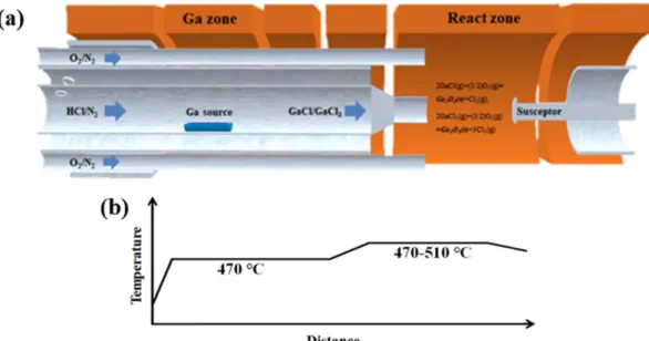
Fig. 1(a) is a schematic of the HVPE equipment used in the study. HVPE is a type of CVD method that reacts at atmospheric pressure in a horizontal reactor. In case of
†Corresponding author E-mail: [email protected]
© 2019, The Korean Microelectronics and Packaging Society
This is an Open-Access article distributed under the terms of the Creative Commons Attribution Non-Commercial License(http://creativecommons.org/
licenses/by-nc/3.0) which permits unrestricted non-commercial use, distribution, and reproduction in any medium, provided the original work is properly cited.
114 Daejang Lee, An-Na Cha, Junseong Park, Hogyun Noh, Youngboo Moon, and Jun-Seok Ha
HVPE, the precursor consisted of GaCl and O2. GaCl was synthesized through a chemical reaction between metallic Ga (6N grade) and HCl gas (5N grade) at 470oC in the Ga source zone of the reactor. The partial pressures of HCl and O2 were 0.25~0.55 kPa and 1~4 kPa, respectively. N2 (6N grade) was used as the carrier gas. GaCl and O2 were sep- arately transferred to the growth zone, where an α-Al2O3 substrate was placed on a quartz glass susceptor. The HVPE equipment was divided into six sections, consisting of the Ga source zone in which Ga and HCl reacted and the growth zone in which α-Ga2O3 was grown by reacting GaCl and O2. The remaining sections served as insulation sections. Fig. 1(b) shows the temperature change according to the distance in the reactor. The temperature of the Ga source zone was fixed at 470oC. The growth zone was heated to a temperature between 460 and 520oC under a N2 flow and it contained O2 at a partial pressure of 1 kPa.
Growth time was fixed at 50 min.
The crystallinity of the resulting α-Ga2O3 thin films was analyzed by high-resolution X-ray diffraction (XRD). The surface morphology of the films was observed by scanning electron microscopy (SEM). The growth rate was deter- mined by cross-sectional SEM. The structural quality was estimated by x-ray rocking curve (XRC) measurements.
The impurity concentration was measured by secondary ion mass spectrometry (SIMS). The optical transmittance spectrum was utilized to determine the energy bandgap, and the baseline was measured with a double-side polished sapphire substrate. and a 45 wt% KOH solution was pre- pared and boiled at 65oC using a hot plate. Then, the α- Ga2O3 thin film was dipped into the solution for 60 min to confirm the density of defects.
3. Results and Discussion
We first studied the optimal temperature to suppress β phase in the temperature range of 470~510oC. Then, we found the optimal III/IV ratio to maximize crystallinity. In the case of Ga2O3, when the temperature exceeded a cer- tain growth temperature, the α phase shifted to the β phase.
The β phase peak was found in the region of about 38.8o.19) Fig. 2(a) shows the XRD 2θ/θ scan profiles of the growth of α-Ga2O3 as a function of growth temperature. For α- Ga2O3 grown from 470 to 510oC, only peaks for α-Ga2O3 were found in the growth region and no peaks for β-Ga2O3 were observed. Moreover, peaks for α-Ga2O3 were not observed at temperatures below 460oC. When the growth temperature reached 520oC, β-Ga2O3 peaks were observed at about 38.3o. This result confirmed that transition from α phase to β phase occurred. Also, the stable temperature for α-Ga2O3 growth by HVPE was 470~510oC.
We also studied the change in crystallinity with respect to the growth zone temperature. Fig. 2(b) shows the XRC profiles of the α-Ga2O3 (0006) diffraction peaks. For Ga2O3 grown at 510oC, only the single crystal α phase was detected and excellent crystallinity at FWHM of 216 arcsec was observed for the (0006) reflection.
However, the crystallinity of α-Ga2O3 rapidly deterio- rated at 520oC. The reason can be confirmed by the graph of Fig. 2(b) As shown in the graph, the α phase disappears at 520oC and the phase transitions to the polycrystalline β phase. Therefore, optimizing the growth temperature is an important factor for obtaining single crystallinity α-Ga2O3. The growth temperature of pure α-Ga2O3 crystals is obtained differently depending on various growth methods.
Fig. 1. (a) Schematic drawing of the HVPE system. (b) Process flow graph of temperature change with distance
Oshima and Fujita reported that using Mist-CVD, β-Ga2O3 was not grown from 470 to 630oC, and that only α-Ga2O3 was grown in this temperature range.7) In contrast, when Ga2O3 films were grown using MBE on c-plane sapphire substrates in the same temperature range, β-Ga2O3 was found at about 38o.20) Such a difference could originate not only from the growth temperature but also from the basic characteristics of each growth method.
Fig. 2(c) shows the results of the experiment to obtain optimal crystallinity through III/VI ratio control. First, we investigated the changes in crystallinity with respect to changes in P(HCl). P(O2) was fixed at 1.00 kPa, while P(HCl) was varied from 0.25 to 0.55 kPa. Under constant P(O2), FWHM decreased as P(HCl) decreased.
Second, Fig. 2(d) shows the change in FWHM with the change in P(HCl). P(HCl) was fixed at 0.45 kPa, while P(O2) was varied from 1.00 to 4.00 kPa. Similar to the
changes in crystallinity observed when P(HCl) was varied, the crystallinity tended to increase as the react gas partial pressure decreased. These results show that excess reactive gas interferes with the binding of GaCl3 and O2 and reduces crystallinity. These growth conditions may differ depending on the temperature of the Ga source zone, the flow rate of the carrier gas, and the capacity of the growth zone. Therefore, we studied the effect of flow rate of the carrier gas on the crystallinity, keeping the temperature of the Ga source zone constant at 470oC.
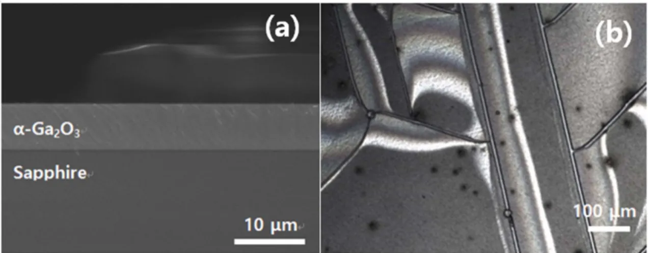
Fig. 3(a) shows an SEM image of a sample α-Ga2O3 thin film grown on a sapphire substrate. The surface of the thin film was mirror-like and transparent. The growth tempera- ture was set at 510oC to suppress the formation of the β phase, and the III/VI ratio was fixed at 4 to ensure single crystallinity. The thickness of the grown film was about 6.891 μm, and no defects or pits were observed on the sur- Fig. 2. XRD scan spectra of samples as functions of growth temperature. (a) 2θ/θ scan profile, (b) XRCs of an α-Ga2O3 film around
(0006), (C) Thin film FWHM variation according to HCl partial pressure and (d) O2 partial pressure.
116 Daejang Lee, An-Na Cha, Junseong Park, Hogyun Noh, Youngboo Moon, and Jun-Seok Ha
face. After the growth, when the sample was taken out of the reactor at a high temperature, a part of the thin film peeled off because of the difference between its thermal expansion coefficient and that of the substrate. Therefore, to prevent this peeling, the temperature was sufficiently lowered to 200oC before taking the sample out of the reac- tor.
Fig. 3(b) is an optical microscope image showing the crystallinity of α-Ga2O3 with respect to etch pit density (EPD). The EPD was found to be as low as about 6.0×104 cm−2. To the best of our knowledge, this value is the lowest EPD obtained for α-Ga2O3 thin films grown by HVPE so far.
Fig. 4 shows the transmittance T of the thin film using a UV-vis spectrometer. Perfect absorption occurred in the region below 238 nm, and in the visible light region, trans- mittance was about 90%. We estimated the bandgap to be 5.21 eV from the (hʋα)2-hʋ plot. It was also confirmed that
the α-Ga2O3 thin film grown on the double-side polished substrate was highly transparent (inset of Fig. 4).
Fig. 5 shows the impurity depth profiles measured in α- Ga2O3 grown on Sapphire substrate by SIMS. The ele- ments [C], [H], [Si], [Al], and [Cl] were scanned. The con- centrations of the typical impurities present in the α-Ga2O3 thin films were found to be as high as 1017 cm−3. [C] and [H] were much lower than the reported values ([H]=
3×1019 cm−3, [C] = 1×1019 cm−3).21) Also, the concentration of [Cl] was found to be [Cl] = 1×1017 cm−3. However, there is no clear evidence that Cl affects the electrical properties of α-Ga2O3. a report by Murakmi et al. has already revealed that Cl does not act in HVPE-grown β-Ga2O3 as a donor.19
4. Conclusions
In this study, α-Ga2O3 crystals with the single crystallin- ity reported so far were grown hetero-epitaxially on a c- plane sapphire substrate using HVPE. We modified the III/
Fig. 3. Images of an α-Ga2O3 layer grown on a sapphire (0001) substrate: (a) cross-sectional image and (b) surface image with respect to etch pit density (EPD).
Fig. 4. Transmittance spectra and a photograph of α-Ga2O3. The inset shows the mirror-like surface.
Fig. 5. Impurity concentrations in α-Ga2O3 measured by SIMS.
FWHM of α- Ga2O3 was about 178 arcsec. EPD measure- ments using KOH solution were performed to confirm the defect density of the thin film; the EPD of the grown thin film was found to be about 6.0×104 cm−2, which is rela- tively low. The result of SIMS measurements showed that [C] and [Cl] were relatively lower than those in α-Ga2O3 grown under the same growth conditions.
The optical transmittance of the thin film was higher than 90% in the visible and near-UV regions. The α-Ga2O3 epitaxial layer exhibited excellent crystallographic proper- ties and smooth surface morphologies, and the bandgap was estimated to be 5.21 eV from the (hʋα)2-hʋ plot. The thickness of the grown thin film was about 6.891 μm. We confirmed that growth of thin films with low impurity con- centration and defect density is possible and the possibility of single crystal growth using HVPE.
Acknowledgments
This work was supported by Priority Research Centers Program through the National Research Foundation of Korea(NRF) funded by the Ministry of Education, Science and Technology (2018R1A6A1A03024334) and Basic Sci- ence Research Capacity Enhancement Project through Korea Basic Science Institute (National research Facilities and Equipment Center) grant funded by the Ministry of Education. (Grant No. 2019R1A6C1010024)
References
1. J. Y. Tsao, S. Chowdhury, M. A. Hollis, D. Jena, N. M. John- son, K. A. Jones, R. J. Kaplar, S. Rajan, C. G. Van de Walle, E. Bellotti, C. L. Chua, R. Collazo, M. E. Coltrin, J. A. Coo- per, K. R. Evans, S. Graham, T. A. Grotjohn, E. R. Heller, M. Higashiwaki, M. S. Islam, P. W. Juodawlkis, M. A. Khan, A. D. Koehler, J. H. Leach, U. K. Mishra, R. J. Nemanich, R. C. N. Pilawa-Podgurski, J. B. Shealy, Z. Sitar, M. J. Tadjer, A. F. Witulski, M. Wraback, and J. A. Simmons, “Ultrawide- Bandgap Semiconductors: Research Opportunities and Chal-
6. M. Higashiwaki, K. Sasaki, A. Kuramata, T. Masui, and S.
Yamakoshi, “Gallium oxide (Ga2O3) metal-semiconductor field-effect transistors on single-crystal β-Ga2O3 (010) sub- strates”, Appl. Phys. Lett., 100, 013504 (2012).
7. K. Sasaki, A. Kuramata, T. Masui, E. G. Víllora, K. Shi- mamura, and S. Yamakoshi, “Device-quality β-Ga2O3 epitax- ial films fabricated by ozone molecular beam epitaxy”, Appl.
Phys. Express., 5, 035502 (2012).
8. M. Higashiwaki, K. Sasaki, T. Kamimura, M. H. Wong, D.
Krishnamurthy, A. Kuramata, T. Masui, and S. Yamakoshi,
“Depletion-mode Ga2O3 metal-oxide-semiconductor field- effect transistors on β-Ga2O3 (010) substrates and temperature dependence of their device characteristics”, Appl. Phys. Lett., 103, 123511 (2013).
9. R. Roy, V. G. Hill, and E. F. Osborn, “Polymorphism of Ga2O3 and the System Ga2O3—H2O”, J. Am. Chem. Soc., 74, 719 (1952).
10. Y. Oshima, E.G. Víllora, and K. Shimamura, “Halide vapor phase epitaxy of twin-free α- Ga2O3 on sapphire (0001) sub- strates”, Appl. Phys. Express., 8, 055501 (2015).
11. S. Fujita, and K. Kaneko, “Epitaxial growth of corundum- structured wide band gap III-oxide semiconductor thin films”, J. Cryst. Growth., 401, 588 (2014).
12. J. J. Tietjen, and J. A. Amic, “The preparation and properties of vapor?deposited epitaxial GaAs1− x P x using arsine and phosphine”, J. Electrochem. Soc., 113, 724 (1966).
13. Y. Oshima, E.G. Víllora, Y. Matsushita, S. Yamamoto, and K.
Shimamura, “Epitaxial growth of phase-pure ε-Ga2O3 by halide vapor phase epitaxy”, J. Appl. Phys., 118, 085301 (2015).
14. R. Kumaran, T. Tiedje, S. E. Webster, S. Penson, and W. Li,
“Epitaxial Nd-doped α-(Al1−xGax) 2O3 films on sapphire for solid-state waveguide lasers”, Opt. Lett., 35, 3793 (2010).
15. Y. Kokubun, K. Miura, F. Endo, and S. Nakagomi, “Sol-gel prepared thin films for ultraviolet photodetectors”, Appl.
Phys. Lett., 90 (2007) 031912.
16. K. Kaneko, H. Kawanowa, H. Ito, and S. Fujita, “Evaluation of Misfit Relaxation in α-Ga2O3 Epitaxial Growth on α-Ga2O3 Substrate”, Jpn. J. Appl. Phys., 51, 020201 (2012).
17. F. Vigué, P. Vennéguès, S. Vézian, M. Laügt, and J.-P. Faurie,
“Defect characterization in ZnO layers grown by plasma- enhanced molecular-beam epitaxy on (0001) sapphire sub- strates”, Appl. Phys. Lett., 79, 194 (2001).
18. M.-G. Ju, X. Wang, W. Liang, Y. Zhao, and C. Li, “Tuning the energy band-gap of crystalline gallium oxide to enhance photocatalytic water splitting: mixed-phase junctions”, J.
118 Daejang Lee, An-Na Cha, Junseong Park, Hogyun Noh, Youngboo Moon, and Jun-Seok Ha
Materials Chem. A., 2, 17005 (2014).
19. H. Murakami, K. Nomura, K. Goto, K. Sasaki, K. Kawara, Q.T. Thieu, R. Togashi, Y. Kumagai, M. Higashiwaki, and A.
Kuramata, “Homoepitaxial growth of β-Ga2O3 layers by halide vapor phase epitaxy”, Appl. Phys. Express., 8, 015503 (2014).
20. T. Oshima, T. Okuno, and S. Fujita, “Ga2O3 thin film growth
on c-plane sapphire substrates by molecular beam epitaxy for deep-ultraviolet photodetectors”, Jpn. J. Appl. Phys., 46, 7217 (2007).
21. K. Akaiwa, and S. Fujita, “Electrical conductive corundum- structured α-Ga2O3 thin films on sapphire with tin-doping grown by spray-assisted mist chemical vapor deposition”, Jpn. J. Appl. Phys., 51, 070203 (2012).