A Compact Active Channel Module Design for Active Phased Array Antenna System
Young-Bae Jung*
Abstract
This paper introduces the T/RX combined compact active channel module which is a key unit of the active phased array antenna(APAA) system. This module is mainly compoased of two parts for TX and RX fabricated on both sides of the active module for size reduction. The TX-part is primarily composed of a 3-stage amplifier, a microstrip phase shifter, a thermal compensation and a power detection circuit. The RX-part is composed of LNAs a microstrip phase shifter and BPFs for TX power rejection. Using the proposed design structure we can realized a compact active channel module having high performance.
Key words: Active channel, phased array, antenna, APAA, satellite communications, phase shifter
* Dept. of Electronics and Control Engineering, Hanbat National University ([email protected], 042-821-1136)
※ This research was supported by Basic Science Research Program through the National Research Foundation of Korea(NRF) funded by the Ministry of Education, Science and Technology (2011-0013213)
Manuscript received Sep. 16, 2013; revised Sep. 18. 2013
; accepted Sep. 23.. 2013
I. Introduction
Since satellite communications can cover wide range, it is inherently suitable for mobile communications. And it has the advantages in propagation conditions compared to terrestrial communications since it suffers from less interference by receiving communication signal directly. In these days, therefore, as mobile direct broadcasting satellite (DBS) service has become widespread, increasing attention is paid to bilateral communication technologies via communication satellites for various purposes[1].
As the first model for satellite communications, Ku-band mobile APAA system was developed already by ETRI in Korea[2-5]. But it is unilateral system for satellite receptions. By the demand for bilateral communication system using satellite, ETRI
launched its development, too. This system can be divided into several functional units including radiator, T/R module, satellite tracking controller (STC) and other operating units.
II. Active Channel Module Design
The roles played by TX-ACB of the T/R module in the antenna system are beam steering for transmit signal, power amplification and function of output power monitor/report. Fig. 1 shows the block diagram of TX-ACB of the T/R module. It has basically four subassemblies to accomplish the functions above mentioned; 4bit microstrip phase shifter (MICPS), temperature compensation circuit (TCC), power amplifier composed of 3-stages and power detection circuit using parallel coupled transmission lines coupler.
Fig. 1. The block diagram of the TX-ACB
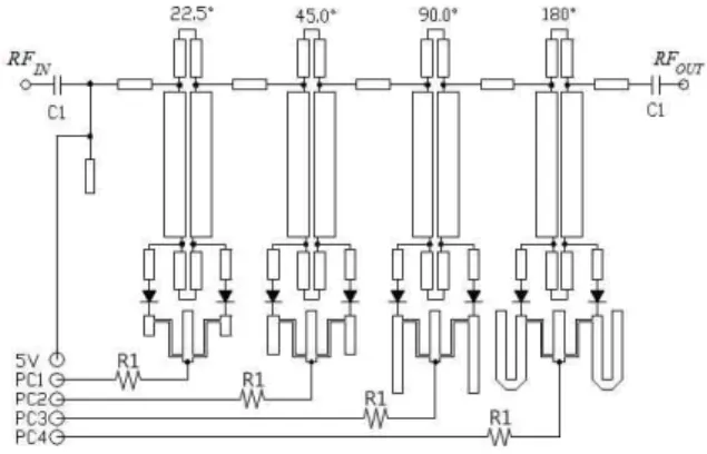
The MICPS was designed for transmit antenna beam steering. Its basic element is modified branch-line coupler that makes use of the form of quarter-wavelength coupler to realize minimum size.
To satisfy system performance of beam tracking, it is composed of four hybrid branch-line couplers for 16 phase states. Each of them includes two pin diodes, and corresponds to 22.5°, 45°, 90° and 180°
respectively. As shown in the schematic diagram Fig. 2, each phase bit is controlled by phase control codes, from PC1 to PC4, coming from the beam steering controller (BSC) of the APAA system.
Fig. 2. The Schematic diagram of the MICPS
Fig. 3. The Schematic diagram of the TCC
(1)
(2)
And, in order to prevent output power from being degraded by the heat generated from internal and external cause, especially power amplifier, modified variable attenuator i.e. TCC was adopted in TX-ACB. The TCC structure of Fig. 3 provides thermal compensating function on the basis of temperature by NTC thermistors, and its in/output matching condition was kept by the isolation ports to which no power is coupled. And, constant output power needed for TX-ACB can be realized by variable forward resistance of pin diodes that are inversely proportional to ID that can be expressed by equation 1 and 2.
For amplification of transmit signal, Power amplifier is lined-up by three GaAs FETs having output power of 0.17 W, 1 W and 4 W respectively, and the line-up has the advantage of low-cost. In RF design, three separate designs of each of them were implemented on the same design concept by RF circuit simulator to which the S-parameters on data sheet for the optimal bias conditions were applied, and several design factors such as stability factor K, available gain circle, input/output matching conditions and so on were checked by the circuit simulator for the inter-stage matching of all stages.
The quarter-wavelength directional coupler was used for output power detection. Its coupling degree, about 35 dB, was decided in the condition that the output power is not influenced by the coupled power, and for the rectification process shottky diode having good performance in X-band was chosen. The minimum available power that can be considered as normal condition is 28 dBm, and the rectified DC voltage of the power is about 0.76V.
RX-ACB of the T/R module plays also several roles in the antenna system such as beam steering for satellite signal reception, low noise power amplification and the function of monitor/report for normal operation. The composition of RX-ACB to accomplish the functions is shown in Fig. 4.
To satisfy the required noise performance, low noise hetero junction FET was chosen. The first LNA was designed by the concept for low noise characteristic above all. But the concept for high
TX RX Ground Plane
gain was implemented in the second and the third LNA designs. Overall design of them including input/output matching circuits was accomplished by using RF circuit simulator, and the bias condition of Vds = 2 V and Ids = 10 mA is needed for the optimal operation of the LNAs. The overall noise temperature of the RX-ACB can be modeled equivalently as shown in Fig. 4 and calculated by equation 3 and 4.
Fig. 4. The Noise Model of the RX-ACB
(3)
where,
(4)
In this diagram, the position of microstrip 7-pole hairpin-line BPF(henceforth, M_BPF) was decided by the viewpoint of noise characteristic and TX-power rejection. By the arrangement, RX-ACB has the possibility that the first two LNAs may be saturated by the leakage power of TX-ACB that is considerable in comparison with the input level of received signal. So, for the protection of the LNA saturation, the mechanic box of T/R module was designed and modified to maximize the isolation between TX and RX-ACB. Fig. 5 shows the assembled T/R module. Its front side includes RF and DC board for TX, and the back side contains them for RX.
(a) Front side(TX-ACB)
(b) Back side(RX-ACB)
(c) Side view of T/R Module Fig. 5. Photograph of assembled T/R module
Fig. 6. Alarm detection circuit for RX-ACB
Of the subassemblies composing RX-part, п-network attenuator made of lumped elements is used for manually changeable power attenuation, and MICPS was designed to be optimized in the operation band of RX by the same design
(a) Output power and its detection voltage for TX-ACB (b) Gain variation by temperature for TX-ACB
(c) Gain variation by phase control for RX-ACB (d) Phase response of RX-ACB by MICPS Fig. 7. Measured results of fabricated active channel module
conception that was applied to the MICPS design of TX-ACB.
Finally, for the supply of constant current and voltage, the stabilized active DC bias circuits were designed. In Fig. 6, alarm detection circuit for RX-ACB is shown. It is composed of two voltage comparators and two voltage dividers to establish acceptable bias range, from VLCAT (Low current alarmt hreshold) to VHCAT (High current alarm threshold). And, by the voltage setting, available drain current is about 72mA ± 20%.
III. Fabrication and Experiement
In order to develop the T/R module, RF boards were fabricated on a 0.508mm-thick
substrate within ±0.02mm etching tolerance. By the consideration of mechanic box design for the isolation between T/RX channel, minimum 104 dB isolation was achieved. Isolation test was accomplished with the normal operation condition that transmitted power level was 35 dBm, and test results were measured at output port of RX-ACB.
In Fig. 7(a), the test results of output power and its detection voltage for TX-ACB are shown. The minimum value of P1-dBc was 35.6 dBm at 7.9 GHz, 36.8 dBm at 8.15 GHz and 36.0 dBm at 8.4 GHz respectively, with minimum gain of 22 dB, and detection voltage at P1-dBc was about 2.1 V.
The characteristic of gain variation by
temperature for TX-ACB is shown in Fig. 7(b). Its measured value was ±0.6 dB compared with maximum gain, and the surface temperature of T/R module ranged from 27 ℃ to 60 ℃. According as the temperature increase, linear gain of TX-ACB decreased, and, at 60 ℃, output power was reached at equilibrium state. In this channel gain test, 30 dB external attenuator was used, and the total cable loss, about 1 dB, was not considered.
As other performances of TX-ACB, the gain variations by phase control and temperature were about ±1.2 dB and ±0.6 dB within operation band.
The phase response of TX-ACB by MICPS was similar to the response of RX-ACB depicted in Fig.
7(c) and (d). The RX-ACB has the minimum gain of 26.5 dB with 1.0dB maximum noise figure at 0-state of MICPS, and the gain variations by temperature and phase control of ±0.51 dB and
±1.65 dB respectively. The phase response of the RX-ACB by MICPS is also shown, and it shows 4-bit operation with the resolution of 22.5° in the phase controllable range of 360°. In RX-ACB, the allowable phase error is ±11.25° at all control steps.
And, overall tests of T/RX-ACB as stated above were accomplished under the same test conditions including equipments and environment.
IV. Conclusion
The T/R module playing several roles was designed and fabricated for the APAA system used in bilateral communications via satellite. It is a key unit of APAA system and composed of TX and RX-ACB. The TX-ACB has the performances of P1-dBc of 35.6 dBm with 22 dB gain. And, for RX-ACB, its linear gain is minimum 26.5dB with 1.0dB noise figure. All of the ACBs include a MICPS with the resolution of 22.5° for satellite tracking, and it was confirmed that the experimental results of the T/R module satisfied the performances required in the APAA system.
References
[1] K. Fujimoto, J. R. James, Mobile Antenna Systems Handbook, Artech House, 1994.
[2] S. Y. Eom, et al., “RACB Design of Ku-band APAA System for Mobile DBS Reception”, 29th European Microwave conference, Munich, Germany, pp. 83-86, Oct. 1999
[3] S. Y. Eom, et al., “Active Channel Blocks of Active Phased Array Antenna for the Vehicular DBS System of Ku-band”, XXVII Moscow ICATT IEEE AP-S, pp. 257-260, Sept. 1998.
[4] S. I. Jeon, J. I. Choi, C. S. Yim, S. P. Lee, A.
V. Shishlov, “Vehicular Active Antenna System with Combined Electronical and Mechanical Beam steering for Reception from DBS in Ku-band”, XXVII Moscow ICATT IEEE AP-S, pp.72-77, Sept. 1998.
[5] S. I. Jeon, et al., “Active Phased Array Antenna for the Vehicular DBS System of Ku-band”, XXVII Moscow ICATT IEEE AP-S, pp. 253-256, Sept.
1998.
[6] G. Gonzalez, Microwave Transistor Amplifiers:
Analysis and Design”, Prentice Hall, Inc., 1997.
BIOGRAPHY
Jung Young-Bae (Member)
1998 : BS degree in Radio Science and Engineering, Kwangwoon University.
2001 : MS degree in Microwave Engineering, KAIST.
2009 : Ph.D degree in Microwave Engineering, KAIST.
2001~2011 : Senior researcher, ETRI
2011~Present: Electronics and control engineering, Hanbat national university