반도체디스플레이기술학회지 제18권 제4호(2019년 12월)
Journal of the Semiconductor & Display Technology, Vol. 18, No. 4. December 2019.
Selective Laser Direct Patterning of Indium Tin Oxide on Transparent Oxide Semiconductor Thin Films
Haechang Lee * , Zhenqian Zhao * , Sang Jik Kwon * and Eou Sik Cho *†
*† Department of Electronics Engineering, Gachon University
ABSTRACT
For a wider application of laser direct patterning, selective laser ablation of indium tin oxide (ITO) film on transparent oxide semiconductor (TOS) thin film was carried out using a diode-pumped Q-switched Nd:YVO 4 laser at a wavelength of 1064 nm. In case of the laser ablation of ITO on indium gallium zinc oxide (IGZO) film, both of ITO and IGZO films were fully etched for all the conditions of the laser beams even though IGZO monolayer was not ablated at the same laser beam condition. On the contrary, in case of the laser ablation of ITO on zinc oxide (ZnO) film, it was possible to etch ITO selectively with a slight damage on ZnO layer. The selective laser ablation is expected to be due to the different coefficient of thermal expansion (CTE) between ITO and ZnO.
Key Words : Selective laser ablation; Indium tin oxide (ITO); Indium gallium zinc oxide (IGZO); Zinc oxide (ZnO);
Coefficient of thermal expansion (CTE)
1. Introduction
1For the realization of simple patterning instead of conventional photolithography, laser direct etching has been used for a formation of electrode in case of indium tin oxide (ITO) layer on glass or flexible substrate [1-6]. The laser direct patterning of ITO has been applied to the fabrication of flat panel display (FPD) such as plasma display panel (PDP) because a higher throughput can be obtained as a result of reduced production time and cost [7,8]. However, the laser direct etching has been only carried out at the first or second process step in the fabrication when only ITO was deposited on glass or flexible substrate. For a wider application of laser direct patterning, it is necessary to etch ITO layer on other semiconductor or insulator layer selectively by using laser direct etching without any damage to remaining semiconductor or insulator layer. When the selective etching of ITO can be obtained, it is expected to apply the laser direct patterning to various electrode formations in electronic devices.
In this work, as transparent oxide semiconductor (TOS)
† E-mail: [email protected]
layers, indium gallium zinc oxide (IGZO) and zinc oxide (ZnO) were deposited on glass substrate, respectively. Then ITO film was deposited on the TOS layers and a Q-switched diode-pumped neodymium-doped yttrium vanadate (Nd:YVO 4 , λ=1064 nm) laser was applied to etch ITO film selectively.
2. Experiment
On two glass substrates, IGZO and ZnO were deposited by radio frequency (RF) sputtering, respectively. IGZO film was deposited with a thickness of 600 Å at a power density of 0.64 W/cm 2 . ZnO film was deposited with a thickness of 500 Å at a power density of 1.2 W/cm 2 . On the IGZO layer and the ZnO layer, ITO was deposited with a thickness of 1000 Å at a power density of 1.8 W/cm 2 by DC magnetron sputtering.
Ar 50 sccm was used in case of IGZO sputtering. Ar 50 sccm and O 2 1.5 sccm were used in case of ZnO and ITO sputtering.
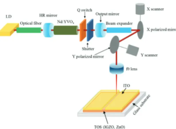
Fig. 1 shows the experimental setup for the laser ablation
of ITO on TOS films. The laser system was a diode-pumped,
single mode, Q-switched Nd:YVO 4 solid-state laser with a
Selective Laser Direct Patterning of Indium Tin Oxide on Transparent Oxide Semiconductor Thin Films 7
Fig. 1. Schematic diagram of laser ablation of ITO on TOS film.
wavelength of 1064 nm, a pulse duration of τ = 10 ns full width at half maximum (FWHM), and a pulse repetition rate within 0~200 kHz. The laser beam was scanned by a built-in galvanometric beam scanning system and de-magnified across the sample area of 100 mm × 100 mm using a F-theta 160 mm focal length lens. In the process of laser direct etching, the processing parameters were the pulse repetition rate and the scanning speed of laser beam. Each of these samples was etched 12 times, with different pulse repetition rates (40 kHz; 60 kHz; 80 kHz) and different scanning speeds (100 mm/s; 500 mm/s; 1000 mm/s; 2000 mm/s). After laser direct etching, the morphologies of the laser ablated patterns were observed by scanning electron microscope (SEM).
Furthermore, the etched depths and the roughness of the scribed grooves were investigated by a stylus profilometer.
3. Results and Discussion
Table 1 shows the results of laser ablated patterns on IGZO/ITO (ITO on IGZO) and ZnO/ITO (ITO on ZnO) samples for various laser beam conditions. As shown in Table 1, at lower repetition rate, it was impossible to obtain continuous scribed line with a higher laser beam scanning speed such as 2000 mm/s.
The scanning electron microscope (SEM) images of laser ablated patterns on IGZO/ITO sample for the laser beam conditions with a scanning speed of 100 mm/s (at repetition rates of 40~80 kHz) and at a repetition rate of 40 kHz (with scanning speeds of 500~2000 mm/s) were shown in Fig. 2 and Fig. 3, respectively. From Fig. 2, the widths of laser
Table 1. Laser ablated multilayer TOS films for various conditions of laser beams. L, DL, S, and N represent line, discontinuous line, spot, and none, respectively.
TOS films Repetition rate(kHz)
Scanning speed (mm/s) 100 500 1000 2000
IGZO/ITO 40 L L L S
IGZO/ITO 60 L L L S
IGZO/ITO 80 L L DL N
ZnO/ITO 40 L L L S
ZnO/ITO 60 L L L DL
ZnO/ITO 80 L L L DL
(a)
(b)
(c)
Fig. 2. SEM images of laser-ablated IGZO/ITO films with a scanning speed of 100 mm/s at various repetition rates: (a) 40 kHz, (b) 60 kHz, and (c) 80 kHz.
ablated lines slightly were decreased at a higher repetition rate.
In case of a higher scanning speed of laser beam, the laser
ablated patterns were changed from continuous lines to spots
Haechang Lee, Zhenqian Zhao, Sang Jik Kwon and Eou Sik Cho 8
(a)
(b)
(c)
Fig. 3. SEM images of laser-ablated IGZO/ITO films at a repetition rate of 40 kHz with various scanning speeds: (a) 500 mm/s, (b) 1000 mm/s, and (c) 2000 mm/s.
and the widths of laser ablated lines were also abruptly decreased as shown in Fig. 2(a) and Fig. 3.
Fig. 4(a) and (b) show the stylus profiles of the laser ablated IGZO/ITO films at a scanning speed of 100 mm/s and 1000 mm/s, respectively. For the laser ablated lines except with a scanning speed of 2000 mm/s, the depth of etched grooves were about 1600 Å. Therefore, it is possible to conclude that both of ITO and IGZO films were fully removed by laser beams. When the laser direct etching was carried out on IGZO monolayer on glass deposited at the same process conditions, it was impossible to investigate the scribble lines on IGZO at a higher scanning speed such as 500 mm/s and 1000 mm/s.
The different results are thought to be due to the different heat transfer. In case of laser direct etching of IGZO monolayer on glass substrate, it is difficult to absorb the thermal energy to melt and remove the IGZO film, because
0 20 40 60 80 100 120 140
-2000 -1500 -1000 -500 0 500 1000
ITO
Glass
Glass/IGZO(600 Å)/ITO(1000 Å)
Th ic kn es s ( Å )
Scan length (µm)
40 kHz 60 kHz 80 kHz
IGZO
(a)
0 20 40 60 80 100 120 140
-2000 -1500 -1000 -500 0 500 1000
ITO
Glass
Glass/IGZO(600 Å)/ITO(1000 Å)
Th ic kn es s ( Å )
Scan length (µm)
40 kHz 60 kHz 80 kHz
IGZO
(b)
Fig. 4. Stylus profiles of laser-ablated IGZO/ITO films with a scanning speed of (a) 100 mm/s and (b) 1000 mm/s.
100 500 1000 2000
0 10 20 30 40 50 60 70 80
Glass/IGZO(600 Å)/ITO(1000 Å)
L ine W idth ( µ m )
Scanning speed (mm/s)
40 kHz 60 kHz 80 kHz
Fig. 5. Line-width of laser-ablated IGZO/ITO films for various scanning speeds of laser beams.
almost laser beam is expected to pass through IGZO and glass substrate.
On the other hand, in case of IGZO/ITO film, it is thought
that IGZO can be easily melt and removed by the absorption
Selective Laser Direct Patterning of Indium Tin Oxide on Transparent Oxide Semiconductor Thin Films 9
of sufficient thermal energy as a result of heat transfer from ITO etching.
Fig. 5 shows the line widths of laser ablated patterns on IGZO/ITO sample for various scanning speeds and various repetition rates of the laser beams. It is noteworthy that the widths of laser ablated patterns decreased at a higher scanning speed or a higher repetition rate. For example, the width of ablated line decreased from 56.86 µm to 23.53 µm when the scanning speed was increased from 100 mm/s to 2000 mm/s at a repetition rate of 40 kHz. In case of the scanning speed of 100 mm/s, the ablated line width was 56.86 µm (40 kHz), 53.92 µm (60 kHz), and 49.51 µm (80 kHz).
It is attributed to the uneven distribution of intensity of laser beam spots formed on the films when each pulse of the laser beam passed though the F-theta lens (as shown in Fig. 1) [9]. In case of a higher scanning speed of laser beam, the
0 20 40 60 80 100 120 140
-2000 -1500 -1000 -500 0 500 1000 1500
Th ic kn ess ( Å )
Scan length (µm) Glass/IGZO (600 Å)/ITO (1000 Å) Glass/ITO (1000 Å)
(a)
0 20 40 60 80 100 120 140
-2000 -1500 -1000 -500 0 500 1000 1500 2000
Th ic kn ess ( Å )
Scan length (µm) Glass/IGZO (600 Å)/ITO (1000 Å) Glass/ITO (1000 Å)
(b)
Fig. 6. Stylus profiles of laser-ablated IGZO/ITO films and ITO film at a repetition rate of 40 kHz with a scanning speed of (a) 100 mm/s and (b) 1000 mm/s.
resident time of laser beam on TOS films is reduced and the energy absorbed by unit area of TOS films is expected to be affected by the scanning speed.
Fig. 6(a) and (b) show the comparison of the stylus profiles of laser ablated IGZO/ITO films and ITO films at a scanning speed of 100 mm/s and 1000 mm/s, respectively. ITO films were deposited on glass at the same process condition. From Fig. 6, it is found that the widths of laser etched patterns of IGZO/ITO were narrower than those of ITO, especially when the scanning speed is 1000 mm/s.
(a)
(b)
(c)
Fig. 7. SEM images of laser-ablated ZnO/ITO films with a scanning speed of 100 mm/s at various repetition rates: (a) 40 kHz, (b) 60 kHz, and (c) 80 kHz.
The SEM images of laser ablated patterns on ZnO/ITO
sample for the laser beam conditions with a scanning speed of
100 mm/s (at repetition rates of 40~80 kHz) and at a
repetition rate of 40 kHz (with scanning speeds of 500~2000
mm/s) were shown in Fig. 7 and Fig. 8, respectively. In case
Haechang Lee, Zhenqian Zhao, Sang Jik Kwon and Eou Sik Cho 10
of a higher scanning speed of laser beam, the laser ablated patterns were changed from continuous lines to spots and the widths of laser ablated lines were decreased, as shown in Fig. 8.
(a)
(b)
(c)
Fig. 8. SEM images of laser-ablated ZnO/ITO films at a repetition rate of 40 kHz with various scanning speeds: (a) 500 mm/s, (b) 1000 mm/s, and (c) 2000 mm/s.
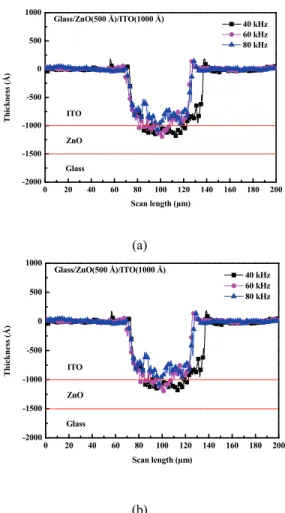
Fig. 9(a) and (b) show the stylus profiles of the laser ablated ZnO/ITO films at a scanning speed of 100 mm/s and 1000 mm/s, respectively. For all the laser ablated lines, the depths of etched grooves were about 1100 Å. Therefore, it is possible to conclude that only ITO films were removed leaving a slight damage (~100 Å) on ZnO film and the selective laser ablation of ITO on ZnO film was achieved. In case of IGZO/ITO, both of ITO and IGZO films were removed during laser ablation though IGZO monolayer was not etched at the same condition of laser beam. It shows that a part of energy was conducted to IGZO film from ITO film
and the ablation of IGZO film was encouraged by this part of energy. Although the heat conduction has also occurred in case of ZnO/ITO, the ZnO film was not removed. It is attributed to high melting spot, and strong ionic bonds of ZnO [10]. The difference of coefficient of thermal expansion (CTE) of ITO and ZnO may be considered as a cause of the different etching mechanism [11,12].
0 20 40 60 80 100 120 140 160 180 200
-2000 -1500 -1000 -500 0 500 1000
Glass
Glass/ZnO(500 Å)/ITO(1000 Å)
T hi ckne ss ( Å )
Scan length (µm)
40 kHz 60 kHz 80 kHz
ITO ZnO
(a)
0 20 40 60 80 100 120 140 160 180 200
-2000 -1500 -1000 -500 0 500 1000
Glass
Glass/ZnO(500 Å)/ITO(1000 Å)
Thi ckne ss ( Å )
Scan length (µm)
40 kHz 60 kHz 80 kHz
ITO ZnO
(b)
Fig. 9. Stylus profiles of laser-ablated ZnO/ITO films with a scanning speed of (a) 100 mm/s and (b) 1000 mm/s.
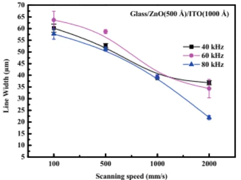
Fig. 10 shows the line widths of laser ablated patterns on
ZnO/ITO for various scanning speeds and various repetition
rates of the laser beam. The widths of laser ablated patterns
decreased at a higher scanning speed. For example, the
ablated line width decreased from 60.2 µm to 36.82 µm when
the scanning speed was increased from 100 mm/s to 2000
mm/s at a repetition rate of 40 kHz. Compared with Fig. 5
Selective Laser Direct Patterning of Indium Tin Oxide on Transparent Oxide Semiconductor Thin Films 11