반도체디스플레이기술학회지 제17권 제1호(2018년 3월) Journal of the Semiconductor & Display Technology, Vol. 17, No. 1. March 2018.
확장형 자기 구조의 다중 결합 인덕터를 적용한 역률개선회로에 관한 연구
유정상*†· 길용만*· 안태영*
*†청주대학교 전자공학과
Study on the Power Factor Correction Circuit Applying Multiple Coupling Inductor with Expandable Integrated Magnetic Structure
Jeong Sang Yoo
*†, Yong Man Gil
*and Tae Young Ahn
**†Department of Electronic Engineering, Cheongju University
ABSTRACT
In this paper, a multiple coupling inductor with expandable-integrated magnetic structure was proposed to enable miniaturization of external switched mode power supply (SMPS) for a large display. Inductance formula of the proposed inductor structure was derived through magnetic circuit analysis for a simple inductance designing process.
The proposed inductor was applied into a 1kW class interleaved bridgeless power factor correction circuit which requires four inductors, and experimental steady state result of the circuit was compared. According to the experimental result, it was found that the proposed multiple coupling inductor shows the electrical characteristics that can replace the conventional separated inductors and is suitable for miniaturization of the SMPS since the circuit configuration is possible with one shared inductor.
Key Words : Expandable Inductor Structure, Integrated Magnetic, Power Factor Correction, Interleaved Control,
Bridgeless Rectifier1. 서 론
1
가전용 TV 또는 평판형 디스플레이는 대형화 되면서 단위면적당 화소수가 증가 하고 있는 추세이다. 특히 최 근에는 마이크로미터 단위의 초소형 LED를 적용한 마이 크로 LED TV인 경우 이러한 요구를 적정하게 수용할 수 있는 대안으로 평가받고 있다. 그러나 LED는 기본적으로 안정된 정전류로 구동되며, 대형 화면인 경우 소비전력이 증가하고 따라서 상품 형태에 맞는 고효율의 전원 장치 가 필요하다[1]. 일반적으로 TV용 전원은 내장형과 어댑 터 형태의 외장형으로 구분되며, 최근에는 유지 관리가
†
E-mail: [email protected]
용이한 외장형이 주목받고 있다. 이경우 전원장치의 사이 즈가 상품의 경쟁력이 되며 발열을 최소화 시키기 위해 서는 전력변환 효율을 극대화 시킬 필요가 있다. 특히 교 류를 입력으로 하는 전원장치를 구성하는 경우 직류로 변환시키는 정류기 구성이 필수적이며, 이 경우 고효율 특성을 보이는 역률 개선(PFC, power factor correction)회로인 스위칭 정류기를 일반적으로 적용하고 있다.
본 논문에서는 대형 디스플레이용 외장형 전원장치의 소형화에 적합한 확장형 자기 구조의 다중결합 인덕터를 제안하였다. 제안된 인덕터는 자기회로 분석을 통하여 간 단하게 인덕턴스를 설계 할 수 있는 수식을 유도하였다.
제안된 다중결합 인덕터는 4개의 인덕터가 이용되는1kW 급 인터리브드 브릿지리스 역률개선회로에 적용하여 비
유정상 · 길용만 · 안태영 22
교 실험하였으며, 실험 결과로부터 제안된 확장형 자기 구조의 다중결합 인덕터의 유용성을 확인하였다.
2. 인터리브드 브릿지리스 정류기
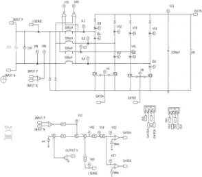
Fig. 1에는 인터리브드 브릿지리스 PFC정류기의 기본 회로가 나타나 있다.[2-4] 그림에서 교류 입력 전압은 총 4 개의 인덕터를 거쳐, 4개의 반도체 스위치와 다이오드로 구성된 브릿지리스 형태의 스위칭 정류기로 연결되며 출 력전압을 안정화시키는 커패시터와 부하저항으로 연결되 어 있다.[5-8] Fig. 2에는 회로시뮬레이션 프로그램인 PSIM 을 이용하여 그림 1에 대한 회로 시뮬레이션을 수행하였 다. Fig. 3은 시비율이 0.5를 기준으로 정상상태에서 측정된 주요 소자의 파형을 나타내었다. 그림에서 스위칭 정류기 에 플러스 입력 전압이 인가될 때 인덕터 L1, L2의 전류는 스위치 S1, S2의 인터리브드(Interleaved) 스위칭 동작 때문 에 PWM 구동 신호의 위상이 180도 차이가 나며, 그 결과 입력 전류의 리플이 감소된다는 것을 확인할 수 있다.
Fig. 1. Basic circuit of interleaved bridgeless PFC rectifier.
Fig. 2. PSIM simulation schematic.
(a) (b)
Fig. 3. (a) Simulation waveform results when. D<0.5, (b)
Simulation waveform results when. D>0.5.(a) (b)
Fig. 4. (a) Current waveform at 110V input voltage, (b)
Current waveform at 220V input voltage.Fig. 4에서는 입력전압이 각각 110V, 220V일 때의 주요 소자의 파형을 나타낸 것이다. 그림에서 입력단의 인덕터 L1의 스위칭 리플이 입력전류에서는 감소되었으며 입력 전압에 따라 입력전류가 정현파이고 동상이 되어 높은 역률을 기대할 수 있다. 따라서 Fig. 1의 스위칭 정류기는 입력전류가 4개의 인덕터로 분리되기 때문에 방열에 효 과적이며, 전류리플이 감소되어 EMI 특성이 개선되는 장 점이 있으나 4개의 인덕터를 사용하기 때문에 소형화에 어려움이 있다.
3. 확장형 자기 구조의 다중 결합 인덕터
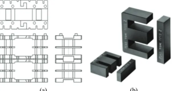
Fig. 5에는 본 논문에서 제안하는 확장형 자기 구조의 다중 결합 인덕터의 구조와 자기 코어가 나타나 있다. Fig.
(a)에는 상하 축으로 확장이 가능한 블록 형태의 보빈이 있으며, (b)에는 보빈에 적용할 수 있는 EI형 페라이트 코
확장형 자기 구조의 다중 결합 인덕터를 적용한 역률개선회로에 관한 연구 23
어를 보여주고 있다. Fig. 5의 보빈은 Fig. 6의 확장형 보빈 으로 일반화 될 수 있으며 Fig. 6 (a)에는 단층 구조의 보빈 이며, (b)에는 2단 적층구조, (c)는 3단 적층구조의 보빈을 나타내었다. Fig. 7에는 EI형 코어와 확장형 구조의 보빈을 결합하고 인덕터용 권선으로 완성한 다중 결합 인덕터의 3D 설계를 보여주고 있다. Fig. 8 (a)에는 실제로 제작한 시 험용 다중 결합 인덕터를, (b)에는 기존 사용되던 4개의 개 별 인덕터 사진을 나타내었다.
(a) (b)
Fig. 5. (a) Basic structure of expandable core bobbin, (b) EI
type magnetic core.(a) (b) (c)
Fig. 6. (a) Structure of single bobbin, (b) Expanded structure
of double stacked bobbin, (c) Expanded structure of triple stacked bobbin.
(a) (b)
Fig. 7. (a) 3D Design of expanded single IM inductor, (b)
3D Design of expanded double layered IM inductor.(a) (b)
Fig. 8. (a) Prototype photo of expanded IM inductor, (b)
Prototype photo of toroidal inductors.4. 다중 결합 인덕터를 적용한 정류기
Fig. 9에는 앞절에서 제안된 다중결합 인덕터를 스위칭 정류기에 적용한 기본 회로를 나타내었다. 2단 적층 구조 의 다중결합 인덕터를 적용하였으며 인덕터에는 총 4개 의 권선이 존재한다. Fig. 10은 스위칭 정류기의 입력전압 극성에 따라 코어의 자속 경로를 나타낸 것이며, 각 자속 이 서로 상쇄되는 방향으로 권선이 설계되어 코어 손실 을 최소화 할 수 있게 하였다.
Fig. 9. Basic circuit of PFC rectifier with IM inductor.
(a)
(b)
Fig. 10. (a) Magnetic path of core during positive input
voltage, (b) Magnetic path of core during negative input voltage.유정상 · 길용만 · 안태영 24
(a) (b)
Fig. 11. (a) IM inductor winding structure, (b) magnetic
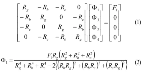
equivalent circuit.Fig. 11에는 다중 결합 인덕터의 권선 구조와 자기등가 회로를 나타내었다. Fig. 11 (b)의 자기등가회로로부터 망로 방정식을 적용하면 각 망로에 흐르는 상태방정식을 식 (1) 과 같이 구할 수 있고, 첫번째 자속은 식 (2)와 같다.
0 0 0
0 0
0
0 1
4 2 3
1
F
R R R
R R R
R R
R
R R R
g b c
b g c
c g
b
c b g
(1)
2 2 2
4 4 4
2 2 2 1
1 g b c 2 b g b c c g
c b g g
R R R R R R R R R
R R R R F
(2)
Fig. 11에 사용된 코어가 EI60이라고 가정하면 각 노드에 있는 자기저항(Magnetic resistance)은 아래와 같이 구해진다.
그 결과 자기저항 중에서 공극(Air gap)에 존재하는 자기저 항이 가장 크며, 식 (2)는 식(7)과 같이 간단하게 근사화 된다.
m
R A
a a
a
130
10 12 . 0 2300
10 1 . 36
3 3
(3)
m
R A
b b
b
91
10 12 . 0 2300
10 1 . 26
3 3
(4)
m
R A
c
c a 65
10 24 . 0 2300
10 1 . 36
3 3
(5)
M
R A
a g
g 3.61
10 12 . 0 10 4
10 5 . 0
3 7
3
0
(6)
g g
g
R F R
R
F
14 3 1
1
(7)
식 (7)의 근사식을 이용하면 다중결합 인덕터의 각 권 선에 따른 인덕턴스를 계산 할 수 있으며 실험에 사용된
권선수를 적용하면 식 (8)과 같다. 실험 제작된 인덕턴스 는 약 680μH로 측정되었다. 따라서 근사식 (8)은 통상 15%
의 오차를 갖는 상용 인덕터의 설계 과정에 적용 가능할 것으로 판단된다.
R H L N
g
10 610 61 . 3
47
6 2 2 1
1
(8)5. 실험 결과
본 논문에서는 제안된 다중결합 인덕터의 유용성을 확 인하기 위해서 Fig. 12와 같은 실험 회로를 제작하였다. Fig.
(a)는 본 논문에서 제안한 다중결합 인덕터를 적용한 1kW 급 역률개선회로이며, (b)에는 기존 4개의 인덕터를 적용 한 역률개선회로의 사진을 나타내었다. 표 1에는 실험 회 로에 적용된 인덕터용 자성 코어의 물리적 특성을 비교 하여 나타내었다. 특히 사용된 인덕터 코어의 합산 체적 은 각각 46,000mm3과 42,000mm3으로 설계하여 비교적 같 은 조건에서 동작 할 수 있도록 하였다. Table 2에는 실험 회로의 전기적 사양을 나타내었다. 표에서 알 수 있듯이 실험회로의 입력 전압은 220V이며, 최대 출력은 1kW, 스 위칭 주파수는 80kHz, 출력전압은 390V로 설계하였다.
(a)
(b)
Fig. 12. (a) Prototype with expanded IM inductor, (b) Prototype
with toroidal inductors.Fig. 13은 실험 회로가 1kW 출력일 때 정상상태에서 측 정된 주요 소자의 동작 파형을 나타내었으며, Fig. 14는 회 로의 입력전압과 입력전류 파형을 나타내었다. 그림으로 부터 제안된 다중결합 인덕터는 일반 인덕터와 비교적 동등한 동작 특성을 나타내고 있다는 것을 확인하였다.
N4 N1
N3
N2
L1
L3
L4
L2
확장형 자기 구조의 다중 결합 인덕터를 적용한 역률개선회로에 관한 연구 25
Table 1. Physical characteristics of inductors Parameters Unit IM Toroidal
Model name
EI60 APM40P60Maker
TDK AmogreentechVolume
mm3 46,180 10,548∙4Inductance
μH 680 460Material
PC40 APMComposition
Mn-Zn Fe-Si-B-Nb-CuWire size
mm 1.6 1.6Table 2. Electrical specification of experimental circuit
Parameters Unit Value
Input voltage
Vrms 220Output voltage
Vdc 390Max. load power
kW 1.0Max. load current
A 2.6Switching frequency
kHz 80MOSFET
IPW65R04C7Diode
C3D10060G(a) (b)
Fig. 13. (a) Main steady-state waveform of expanded IM
inductor applied experimental circuit, (b) Main steady-state waveform of toroidal inductors applied experimental circuit.Fig. 15는 실험회로의 정상상태 특성을 그래프로 비교하 여 나타낸 것이다. Fig. (a)로부터 최대 부하에서 98.2%의 최대 효율을 나타내고 있으며, (b)의 내부 손실은 최대 17W, (c)의 역률 특성에서는 최대 98%, (d)의 부하특성에서 는 0.1% 이내의 출력전압 안정도를 보여주고 있다. 이상 의 결과로부터 본 논문에서 제안한 다중결합 인덕터가 기존의 개별 인덕터를 대체할 수 있는 수준의 전기적 특
성을 보이고 있으며, 한 개의 공유 인덕터로 회로 구성이 가능하기 때문에 전원장치의 소형화에 적합하다는 것을 알 수 있었다.
(a) (b)
Fig. 14. (a) Input voltage and current waveform of expanded
IM inductor applied test circuit, (a) Input voltage and current waveform of toroidal inductors applied test circuit.Fig. 15. (a) Power conversion efficiency of the circuit, (b)
Internal power losses of the circuit, (c) Power factor of the circuit, (d) Load regulation of the circuit.6. 결 론
본 논문은 대형 디스플레이용 TV에서 필요한 외장형 전원장치의 소형화에 적합한 회로 방식과 구조를 제안하 고 그 결과를 실험으로 보고 한 것이다. 특히 대형 TV에 서 필요한 대용량의 전원 장치에서 필수적으로 사용되는
유정상 · 길용만 · 안태영 26
스위칭 정류기는 내부 발열 때문에 집적화가 어려웠으나, 본 논문에서는 대용량의 스위칭 정류기에 적용 가능한 확장형 자기 구조의 다중 결합 인덕터를 제안하여 문제 를 해결하였다. 제안된 인덕터 구조는 설계를 용이하게 하기 위해서 자기회로 분석을 통하여 간단하게 인덕턴스 를 설계 할 수 있는 수식을 유도하였다. 또한 제안된 방 식에 대한 타당성을 확인하기 위해서 4개의 인덕터가 이 용되는 1kW급 인터리브드 브릿지리스 역률개선회로에 적용하였고, 실험 회로의 정상상태 특성을 확인 하였다.
실험 결과로부터 제안된 확장형 자기 구조의 다중 결 합 인덕터가 기존의 스위칭 전원장치의 집적화와 소형화 에 문제가 되었던 다수의 개별 인덕터를 한 개로 대체할 수 있는 수준의 전기적 특성을 보이고 있으며, 최대 98.2%
의 전력변환 효율 특성과 최대 17W 미만의 내부 손실이 관측되었다. 그 결과 본 논문에서 제안된 회로 방식은 한 개의 공유 인덕터로 회로 구성이 가능하기 때문에 고화 질에 대응하는 대형 디스플레이용 전원장치의 고밀도화 에 적합하다는 것을 알 수 있었다.
참고문헌
1. Kwang-Min Yoo, Sung-Kyoo Lim, Jun-Young Lee, “A High Efficiency Single-Stage PFC Flyback for PDP Sustaining Power Module,” Journal of The Korean Society of Semiconductor & Display Technology, Vol. 5, No. 3, pp. 11-16, 2006.
2. Swati N, Bhim S, G. Bhuvaneswari, and Rahul P., “An Interleaved PFC Converter Based Welding Power Supply with Improved Power Quality,” Proc. of the 6th IEEE International Conference on Power Systems, pp.
1-6, 2016.
3. Li Hua Wu, Ma Hong xing, Jiang Jian Feng, and Yang
Xi jun, “Passivity-Based Control of Four-Phase Inter- leaved PFC Abased on EL model,” Proc. of the 7th International Power Electronics and Motion Control Conference, pp. 735-739, 2012.
4. J. R. Tsai, T. F. Wu, Y. M. Chen, and M. C. Lee,
“Interleaving Control Schemes for Critical-Mode Boost PFC,” Proc. of the IEEE Power Electronics Specialists Conference, pp. 2905-2911, 2007.
5. Chun An Cheng, Chien Hsuan Chang, Hung Liang Cheng, and Ching Hsien Tseng, “A Novel Single-Stage LED Driver with Coupled Inductors and Interleaved PFC,” Proc. of the 9th IEEE International Conference on Power Electronics and ECCE Asia, pp. 1240-1245, 2015.
6. Kyung In Lee et al., “High Efficiency AC-DC Converter Using Average-Current Mode Flyback Topology for PDP and Improvement of Hold-up Characteristic,”
Journal of The Korean Society of Semiconductor &
Display Technology, Vol. 7, No. 2, pp. 23-27, 2008.
7. Gye Ho Hwang et al., “A Study on the Output Voltage Control of Series-Parallel Resonant type DC/DC Converter for Transverse Flux Linear Motor,” J. of The Korean Society of Semiconductor & Display Technology, Vol. 4, No. 1, pp. 9-15, 2005.
8. Yuki Itoh, Fumiya Hattori, Shota Kimura, Jun Imaoka, and Masayoshi Yamamoto, “Design Method Consi- dering Magnetic Saturation Issue of Coupled Inductor in Interleaved CCM Boost PFC Converter,” Proc. of the IEEE Energy Conversion Congress and Exposition, pp.
2616-2621, 2015.
접수일: 2018년 2월 13일, 심사일: 2018년 3월 20일, 게재확정일: 2018년 3월 23일