CMOS-Memristor Hybrid 4-bit Multiplier Circuit for Energy-Efficient Computing
Huan Minh Vo
*, Son Ngoc Truong
**, Sanghak Shin
**, Kyeong-Sik Min
**★Abstract
In this paper, we propose a CMOS-memristor hybrid circuit that can perform 4-bit multiplication for future energy-efficient computing in nano-scale digital systems. The proposed CMOS-memristor hybrid circuit is based on the parallel architecture with AND and OR planes. This parallel architecture can be very useful in improving the power-delay product of the proposed circuit compared to the conventional CMOS array multiplier. Particularly, from the SPECTRE simulation of the proposed hybrid circuit with 0.13-mm CMOS devices and memristors, this proposed multiplier is estimated to have better power-delay product by 48% compared to the conventional CMOS array multiplier. In addition to this improvement in energy efficiency, this 4-bit multiplier circuit can occupy smaller area than the conventional array multiplier, because each cross-point memristor can be made only as small as 4F2.
Key words: Memristors, CMOS-memristor hybrid circuits, Energy-efficient computing, Multiplier, CMOS digital circuit
* Dept. of Electrical and Electronics Engineering, the University of Technical Education, Ho Chi Minh City, Vietnam. [email protected], +84-909437522
**Dept. of Electronics Engineering, Kookmin University
★Corresponding author
※The work was financially supported by NRF-2011-220-D00089, NRF-2011-0030228, NRF-2013K1A3A1A25038533, BK Plus with the Educational Research Team for Creative Engineers on Material-Device-Circuit Co-Design (Grant No:
22A20130000042), funded by the National Research
Foundation of Korea (NRF).
NRF-2013R1A1A2A10064812. The CAD tools were supported by IC Design Education Center (IDEC), Daejeon, Korea.
Manuscript received Dec. 26, 2013;revised Jun. 9, 2014;accepted Jun. 10. 2014
I. Introduction
As CMOS technology gets closer to the end of Moore’s law, many researchers have been trying to find some new emerging devices that can survive beyond the end of device scaling scenario [1]. Among many emerging new devices, memristor which was theoretically introduced in 1971 [2] and later experimentally found in 2008
[3] is widely considered as a strong candidate for future post-CMOS devices. Actually, memristors were simply understood as a kind of resistance-change memories that could store the data by resistance change. For example, we can store ‘0’ by Low Resistance State (LRS) and ‘1’
by High Resistance State (HRS), respectively. For many years, various kinds of resistance-change memories have been developed because they are thought to be implementable simply on the cross points between two orthogonal metal lines [4], [5], [6]. The cross-point architecture is indispensable in achieving high-density memory beyond the end of Moore’s law. It occupies only as small as 4F2. Here F means a minimum feature size in a given process technology. In addition to this high-density implementation, memristors can be easily made on top of Silicon devices [7]. This process compatibility with CMOS technology makes it possible to realize hybrid circuits of
CMOS and memristors. The hybrid
CMOS-memristor circuits can be very useful in mitigating the recent problems of CMOS digital circuits such as low energy efficiency and poor
device scalability. In this paper, we propose a CMOS-memristor hybrid circuit with 4-bit multiplication for energy-efficient computing. Here, this proposed multiplier is verified to have 48%
better energy efficiency than the conventional CMOS array multiplier. In addition to this improvement in energy efficiency, this 4-bit multiplier circuit can occupy smaller area, compared to the conventional CMOS array multiplier, because each cross-point memristor can be made with as small as 4F2.
II. New Architecture 1. The conventional CMOS array multiplier.
0 1 2 3 4 5 6 7
3 0 3 1 3 2 3 3
2 0 2 1 2 2 2 3
1 0 1 1 1 2 1 3
0 0 0 1 0 2 0 3
0 1 2 3
0 1 2 3
_____
__________
__________
__________
. . . .
. . . .
. . . .
. . . .
_____
__________
__________
__________
p p p p p p p p
b a b a b a b a
b a b a b a b a
b a b a b a b a
b a b a b a b a
b b b b
a a a a
´
Fig. 1. (a) The multiplication of two 4-bit numbers (b) The block diagram of 4x4-bit CMOS array multiplier Figure 1 shows the multiplication of two 4-bit numbers and the diagram of 4x4-bit CMOS-based array multiplier which consists of 16 ANDs, 9 full adders, and 3 half adder logics to multiply two
4-bit unsigned binary numbers, a3a2a1a0 and b3b2b1b0. Each aibj in Fig. 1(a) is realized using an AND gate. Each output bit is calculated by adding the appropriate aibj in respective column and the carry-in bit from the previous column. To calculate the final 8-bit output, we have to wait for the maximum delay time which includes the propagating times of sum and carry calculation in the adder blocks.
2. Memristor based crossbar logic (MBCL) One of well-known parallel structures to implement the combinational logic is programmable logic device (PLD) which consists of a programmable AND plane linking to a programmable OR plane (PLA) or a fixed OR plane (PAL). Fig. 2 shows the memristor based crossbar logic that works as a PLA structure to implement the logic function in sum-of-product form. In the crossbar array, high and low resistance state (HRS, LRS) memristors represent the open and closed connections. For instance, in Fig. 2, the first row is connected with A’ and B’ by LRS. Here A’ means the complement of A. The other inputs such as A, B, etc are connected to the first row by HRS. This configuration of the first row can realize the function of A’B’. Here, when both A=0 and B=0, A’B’ can be 1. In the other cases, A’B’ should be 0.
Fig. 2. The conceptual schematic for memristor-based crossbar logic (MBCL), where the left array works as an AND plane and the right array performs OR function
0 1 1 0 0 1 0 1 0 1 0 1
0 1 1 0
B B A B A A B B A B A A
B A B A 1 P
+ +
+
=
Å
>=
<
.
(1) The right array in Fig. 2 realizes the OR plane.
For the first column, F0, in the OR plane, F0 can be 1, when either A’B’ or AC’ is 1. Hence F0 can be expressed with F0=A’B’+AC’, as indicated in Fig. 2.
3. The proposed hybrid circuit of CMOS and Memristor for 4-bit multiplier
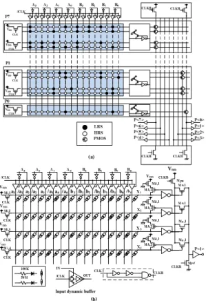
Fig. 3. The proposed MBCL of 4x4-bit dynamic multiplier (a) The block diagram of 4x4-bit dynamic multiplier based on memristor-CMOS hybrid circuit. (b) The detailed circuit for calculating the partial product of P<1>
Figure 3(a) shows the proposed hybrid circuit of the CMOS-memristor 4x4-bit multiplier. The circuit is composed of the AND plane and OR plane. Here A0, A1, A2, and A3 are the A input vector. Similarly, B0, B1, B2, and B3 are the input B vector. CLK and CLKB are the clock and inverted clock signals.
P<0>, P<1>, P<2>, P<3>, P<4>, P<5>, P<6>, and P<7> are the partial products. In Figure 3(a), the memristor array acts as the programmable AND
plane. Each cross point in AND plane is realized by a rectifying memristor that has high resistance state (OFF state) or low resistance state (ON state). The OR plane is implemented by the dynamic-type circuit, as shown in right in Figure 3(a).
The detailed circuit of the partial product, P<1> is shown in Fig. 3(b). P<1> can be calculated with
Four min-term are used to implement the combinational expression represented in Equation (1). Each min-term is realized by each row. For example, if we look at the first row of Figure 3(b), /a1, a0, and b1 are connected with the first row by LRS not HRS. It means that the first row in Figure 3(b) represents the min-term, A1A0B1. Similarly, the second, third, and fourth rows can also represent the other min-terms in Equation (1).
The operation of the proposed memristor-based multiplier in Figure 3(b) is divided into two phases that are called the pre-charge phase and evaluation one. In the pre-charge phase, CLK is held at low level. The input PMOS transistors, Mi,1 to Mi,4 are turn on to charge the row voltages, X1, to X4, by VDD. The input dynamic buffers placed at the top of columns are off with their outputs are high to keep the row voltages high during the pre-charge phase. The PMOS keeper transistors, Mk,1 and Mk,2 are employed to prevent X1, X2, X3, and X4 from being discharged during the evaluation phase. In the evaluation phase, all the input buffers are on. Four min-terms in Equation (1) are decided by the row voltages of X1, X2, X3, and X4. The inverting buffer and the PMOS transistor placed at the end of each row perform the OR function.
III. Simulation and results The simulation results were obtained by the SPECTRE simulator that is provided by Cadence
0 1 1 4
0 0 1 3
0 1 0 2
1 0 1 1
b b a X
b a a X
b b a X
a a a X
=
=
=
=
(2) Design Systems Inc. In this work, the
memristor-CMOS hybrid circuits were simulated by SPECTRE using the memristor’s Verilog-A model [8], [9] and the CMOS model parameters which were given by SAMSUNG 0.13-mm process technology.
Fig. 4. The timing diagram of the proposed memristor-based 4-bit multiplier in two operating cycles, the first cycle represents multiplying 0011 with 0010, the second one is multiplying 0000 with 0000.
Figure 4 shows the timing diagram of the proposed memristor-based 4-bit multiplier in two clock cycles. In the first cycle, two numbers of 0011 and 0010 are applied to the inputs A and B as multiplier and multiplicand, respectively. In the pre-charge phase, all columns are held by VDD
regardless of the inputs A and B by turning off the input dynamic buffers. The row voltages of X1, X2, X3, and X4 are charged to VDD by turning on the PMOS transistors Mi,1 to Mi,4 in Fig. 3(b). During the pre-charge phase, the partial-product nodes, P<0>, P<1>, P<2>, P<3>, P<4>, P<5>, P<6>, and P<7> are low, because the NMOS transistor, Mpd is on. During the evaluation phase, the input dynamic buffers are on thus a3, a2, a1, and a0 can have 1 or 0 according to the input vector of A3, A2, A1, and A0. /a3, /a2, /a1, and /a1 are the complements
of a3, a2, a1, and a0, respectively, as shown in Figure 3(b). Similarly, b3, b2, b1, and b0 are decided by the input vector of B3, B2, B1, and B0, respectively. /b3, /b2, /b1, and /b0 are the inverted version of b3, b2, b1, and b0. During the evaluation phase, the row voltages of X1, X2, X3, and X4 can be calculated with the following Boolean expressions, in Eq. (2).
From the equation (2), when the input vectors A and B are 0011 and 0010, respectively, only the row voltage on X2 can be high, among the row voltages of X1, X2, X3, and X4. If X2 node becomes high during the evaluation phase, the partial product of P<1> can also be high, as shown in Figure 4. In the second operating cycle, when the input vectors of A and B are 0000 and 0000, all the partial products from P<7> to P<0> become 00000000.
Figures 5(a), (b), and (c) show the comparison between the conventional CMOS array multiplier and the proposed memristor-based multiplier in
0.8 1.0 1.2 1.4 1.6
400 800 1200 1600 2000 2400 2800
Rreset=50M Rset=100K Roff=500M T=27oC
Delay (ps)
Voltage supply (V) The CMOS array multiplier The dynamic memristor multiplier
0.8 1.0 1.2 1.4 1.6
50 100 150 200 250 300 350 400
Rreset=50M Rset=100K Roff=500M T=27oC
Power (uW)
Voltage supply (V) The CMOS array multiplier The dynamic memristor multiplier
0.8 1.0 1.2 1.4 1.6
500 1000 1500 2000 2500 3000
Rreset=50M Rset=100K Roff=500M T=27oC
Power-delay product (mWXps)
Voltage supply (V) The CMOS array multiplier The dynamic memristor multiplier
Fig. 5. The comparison of the conventional CMOS array multiplier and the proposed memristor-based multiplier in term of (a) the power consumption, (b) the delay time, and (c) the power-delay product
terms of the power consumption, the power-delay product, and the delay time. In Fig. 5 (a), the multiplied input vectors of A x B are changed between 0000 x 0000 and 1111x1111. In the simulation, the operating frequency is fixed by 100 MHz and the supply voltage is varied from 0.8V to 1.6V. The proposed circuit consumes larger power by 15% on average compared to the conventional CMOS array multiplier. However, the proposed circuit shows shorter delay time compared to the conventional array multiplier, as shown in Fig. 5(b).
The shorter delay time of the proposed circuit is mainly caused by the shorter signal path that is composed of only AND plane and OR plane in the proposed circuit in Figure 3(a). On the contrary, the convention CMOS array multiplier has much longer signal path that includes many logic gates and many 1-bit adders to deliver the carry signal calculated by the present-stage adder to the following stage. Fig. 5(c) compares the power-delay product between the conventional CMOS array multiplier and the proposed CMOS-memristor hybrid multiplier. The power-delay product of the proposed multiplier is estimated smaller by 48% compared to the conventional CMOS array multiplier.
IV. Conclusion
In this paper, we proposed the CMOS-memristor hybrid circuit with 4-bit multiplication for energy-efficient computing. The proposed circuit is based on the parallel architecture with AND and OR planes. This parallel architecture can be very useful in improving the power-delay product of the proposed circuit compared to the conventional CMOS array multiplier. Particularly, from the simulation of the proposed hybrid circuit with 0.13-mm CMOS devices and memristors, this proposed multiplier is estimated to have better power-delay product by 48% compared to the conventional CMOS array multiplier. In addition to this improvement in energy efficiency, this 4-bit multiplier circuit can occupy smaller area than the conventional array multiplier, because each cross-point memristor can be made as small as 4F2.
References
[1] International Technology Roadmap for Semiconductors (ITRS) in 2011.
[2] L. O. Chua, "Memristor-the missing circuit element," IEEE Trans. Circuit Theory, vol. 18, pp.
507-519, Sep. 1971.
[3] D. B. Strukov, G. S. Sinder, D. R. Stewart, and R. S. Williams, "The missing memristor found,"
Nature, vol. 453, pp. 80-83, May 2008.
[4] A. Flocke and T. G. Noll, "Fundamental analysis of resistive nanocrossbars for the use in hybrid nano/CMOS-memory," inProc. 33rd Eur. Solid-State Circuits Conf. ,2007, pp.328-331.
[5] C. Kügeler, M. Meier, R. Rosezin, S. Gilles, and R. Waser, "High density 3D memory architecture based on the resistive switching effect," Solid State Electron, vol. 53, no. 12, pp. 1287-1292, Dec. 2009.
[6] J. Liang and H. -S. Philip Wong, "Cross-point memory array without cell selectors-device characteristics and data storage pattern dependencies," IEEE Trans. Electron Device, vol.
57, no. 10, pp. 2531-2538, Oct. 2010.
[7] C. J. Chevallier, C. H. Siau, S. F. Lim, S. R.
Namala, M. Matsuoka, B. L. Bateman, and D.
Rinerson, "A 0.13 μm 64Mb multi-layered conductive metal-oxide memory," ISSCC, Dig. Tech.
Papers, pp. 260-261, Feb. 2010.
[8] S. J. Ham, H. S. Mo, and K. S. Min,
"Low-power VDD/3 write scheme with inversion coding circuit for complementary memristor array,"
IEEE Trans. Nanotechnology, vol. 12, no. 5, pp.
851-857, Sep. 2013.
[9] J. M. Choi, S. H. Sin, and K. S. Min, "Practical implementation of memristor emulator circuit on printed circuit board," Journal of IKEEE, vol. 17, no. 3, pp. 324-331, Sep. 2013.
BIOGRAPHY
Huan Minh Vo (Student member)
2005, 2007: B.S and M.S.E.E degrees in Electronics and Communication Engineering from the Ho Chi Minh City University of Technology, Vietnam 2013: Ph.D. degree in Electrical Engineering from Kookmin University, Seoul, Korea.
He is currently working as a lecturer at the Electrical and Electronics Engineering Department of The University of Technical Education, Ho Chi Minh City, Vietnam
Son Ngoc Truong (Student member) 2006, 2011 : B.S. and M.S.
degrees in Electronics Engineering from The University of Technical Education, Ho Chi Minh City, Vietnam
He is currently working toward the Ph.D degree at Kookmin University, Seoul, Korea.
Sanghak Shin (Student member)
2013 : BS degree in Electrical Engineering, Kookmin University.
He is currently working toword the Master’s degree of Electrical Enginerring at Kookmin University, Seoul
Kyeong-Sik Min (Life Member)
1991: BS degree in Electronics Engineering, Korea University, Seoul, Korea
1993: MS degree in Electrical Engineering, Korea Advanced Institute of Science and Technology (KAIST), Daejeon, Korea
1997: Ph.D degree in Electrical Engineering, Korea Advanced Institute of Science and Technology (KAIST), Daejeon, Korea
1997~2001: Senior Research Engineer, Hynix Semiconductor Inc., Cheongju, Korea
2001~2002: Research Associate, University of Tokyo, Tokyo, Japan
2002~2014: Professor, Kookmin University, Seoul, Korea