1. Introduction
Ternary and quarternary chalcopyrite compounds, such as CuInSe
2(CISe), Cu(In,Ga)Se
2(CIGSe), CuIn(Se,S)
2(CISeS), and CuGaSe
2(CGSe), have attracted considerable attention as excellent materials in inorganic thin film solar cells due to their high absorption coefficients (~10
5cm
-1) and low cost
1, 2). A high conversion efficiency near 20% was achieved with a CIGSe solar cell of a laboratory scale prepared by a vacuum process
3, 4). CISe or CIGSe films can be prepared by various methods including coevaporation
5), sputtering
6), electrodeposition
7), spraying
8), printing
8), molecular beam epitaxy
9), and so on.
Among these, the electrodeposition has been considered a promising approach from the view points of a non-vacuum and low-cost process, formation of a dense and smooth film, and large area production. CIGSe solar cells prepared by electro- deposition have already reached efficiencies over 11.5% on a laboratory scale and of around 7% on a module scale
10). By
adding the physical vapor deposition (PVD) of In and Ga onto the electrodeposited CIGSe film to adjust the atomic ratios of Cu, In, Ga, and Se, an enhanced cell efficiency over 15% was achieved
11, 12). However, these cells have a configuration con- sisting of glass/Mo/CIGSe/CdS/ZnO, which still needs some cost-intensive vacuum steps, such as sputtering of Mo, i-ZnO and Al-doped ZnO. A superstrate structure, which is the reverse of conventional figures, has been proposed for a cheaper process for CIGSe cells. Superstrate-type cells prepared by the evapora- tion technique showed efficiencies over 8%
13, 14), and ones prepared by electrodeposition of CISe films on In
2Se
3yielded efficiencies of 2.9~3.6%
15-18).
In order to produce high-efficiency CISe or CIGSe solar cells by electrodeposition, there are a number of difficulties to be overcome, including the structural and morphological properties of films, the control of compositional depth profile, and the avoidance of co-deposition of oxides. In particular, the growth of undesirable secondary phases, representatively copper selenides (Cu
2-xSe), usually leads to the formation of Cu-rich films
19). The excessive Cu
2-xSe phases are highly conductive and apt to produce shunt paths, which negatively influence the
Effect of Complexing/Buffering Agents on Morphological Properties of CuInSe 2 Layers Prepared by Single-Bath
Electrodeposition
Hana Lee
1,3)․ Wonjoo Lee
2)․ Kyungwon Seo
1)․ Doh-Kwon Lee
3)․ Honggon Kim
3)*
1)
Department of Chemical Engineering, Ajou University, Suwon 442-749, Korea
2)
Samsung Advanced Institute of Technology, Yong-In 446-712, Korea
3)
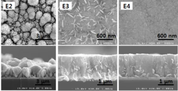
![Fig. 6. SEM images of CISe films with same concentrations of sulfamic acid and potassium biphthalate; [B3] 5 mM each, [B4] 7 mM each, [B5] 10 mM each; (Upper) surface, (Lower) cross-section](https://thumb-ap.123doks.com/thumbv2/123dokinfo/5271022.634979/5.892.486.786.105.253/images-concentrations-sulfamic-potassium-biphthalate-upper-surface-section.webp)