Vol. 23, No. 8 (2013)
430
양자점 층의 미세구조 형상이 양자점 LED 전계 발광 특성에 미치는 효과
윤성룡
* , **
·전민현*
·이전국** †
*
인제대학교 나노시스템공학과, **
한국과학기술연구원 계면제어연구센터Effect of Microstructure of Quantum Dot Layer on Electroluminescent Properties of Quantum Dot Light Emitting Devices
Sung-Lyong Yoon* , **, Minhyon Jeon* and Jeon-Kook Lee** †
*Department of Nano-system Engineering, Inje University, Gimhae-si 621-749, Korea
**Interface Control Research Center, Korea Institute of Science and Technology, Seoul 136-791, Korea
(2013년 7월 15일 접수 : 2013년 7월 31일 최종수정 : 2013년 8월 1일 채택)
Abstract
Quantum dots(QDs) with their tunable luminescence properties are uniquely suited for use as lumophores in light emitting device. We investigate the microstructural effect on the electroluminescence(EL). Here we report the use of inorganic semiconductors as robust charge transport layers, and demonstrate devices with light emission. We chose mechanically smooth and compositionally amorphous films to prevent electrical shorts. We grew semiconducting oxide films with low free-carrier concentrations to minimize quenching of the QD EL. The hole transport layer(HTL) and electron transport layer(ETL) were chosen to have carrier concentrations and energy-band offsets similar to the QDs so that electron and hole injection into the QD layer was balanced. For the ETL and the HTL, we selected a 40-nm-thick ZnSnOx with a resistivity of 10Ω·cm, which
show bright and uniform emission at a 10 V applied bias. Light emitting uniformity was improved by reducing the rpm of QD spin coating.At a QD concentration of 15.0 mg/mL, we observed bright and uniform electroluminescence at a 12 V applied bias.The significant decrease in QD luminescence can be attributed to the non-uniform QD layers. This suggests that we should control the interface between QD layers and charge transport layers to improve the electroluminescence.
Key words
quantum dot LEDs, inorganic semiconductor, spin-coating, electroluminescence.1.
서 론크기에 따라 밴드갭의 조절이 가능한 양자점(quantum dot) 은 색 조정이 가능하며, 좁은 반가폭(full-width at half-maximum value, FWHM) 으로 가시광선 영역에서 높은 발광 효율의 디스플레이 광원으로 활용 가능하다.
휘발성 용매에 분산된 콜로이드 공정으로 제조된 양자 점 발광소자(quantum dot light emitting devices, QD- LED) 는 대면적 제작이 용이하여 면광원으로 사용이 가 능한 소자이다.
1-6)전도성 고분자 전하수송 층을 사용하여 최고의 발광 효 율을 나타내는 QD-OLED(quantum dot-organic light emit-
ting devices) 의 양자 효율을 높이기위해 평탄한 양자점 배열에 관한 연구가 활발히 이뤄지고 있다.
7)그러나, 전 도성 고분자 전하수송 층 이용 소자의 경우, 공기 중의 수분에 의해 소자의 특성이 저하되고 수명이 짧아지는 단점이 있어 별도의 패키징 공정이 필요하다.
따라서, 공기 중에서도 화학적으로 안정하며 가시광선 영역에서 투명하고 우수한 전기적 특성을 보이는 금속 산화물 전하수송 층 이용 QD-LED 연구가 활발하게 진 행되고 있다. 그리고 높은 양자 효율을 구현하기 위해 조밀하게 단층으로 양자점을 배열하여 저항성 전력 감 소를 최소화하는 연구가 활발하다.
8)그러나, 금속 산화 물 층의 표면 형상이 불균질하면, 양자점 발광소자의 광
†Corresponding author
E-Mail : [email protected] (J.-K. Lee, KIST)
©
Materials Research Society of Korea, All rights reserved.This is an Open-Access article distributed under the terms of the Creative Commons Attribution Non-Commercial License (http://creative- commons.org/licenses/by-nc/3.0) which permits unrestricted non-commercial use, distribution, and reproduction in any medium, provided the original work is properly cited.
특성이 저하된다.
9,10)이러한 광특성 저하는 산화물 반도 체 다층 구조에서 양자점으로 전하가 전달될 때, 광이 득 특성의 변화에 의한 것으로 알려져 있다.
11,12)그런데 고분자 전하수송 층 위에 규칙적이고 조밀한 육 방정 결정 구조의 단층 양자점 배열에 의한 전계발광 (electroluminescence, EL) 특성 향상에 관한 연구 결과 는 보고된 바 있으나,
3)금속산화물 위에 형성된 양자점 미세구조 제어에 의한 EL 특성 향상에 대한 연구는 미 흡하다. 일반적으로 전도성 고분자 전하 수송 층 위에 형성된 양자점 발광소자에서 양자점의 농도가 4.8 mg/mL 일 때와 16.0 mg/mL일 때의 스핀 코팅 coverage가 각각 25 % 와 88 %로 나타났으며, 농도가 48.0 mg/mL일 때 부 분적으로 다층으로 도포되었다.
3)본 연구에서는 금속산화물 전하 수송 층 위에 형성된 양자점 층의 미세구조 변화에 따른 EL 특성의 변화를 관찰하였다.
2.
실험 방법본 연구에서 제조한 QD-LED 소자의 구조 및 제작 순 서는 Fig. 1과 같다. 전하 수송 층은 패턴된 Indium tin oxide(InSnO
x, ITO) 유리기판 위에 쉐도우 마스크를 사용 하여 RF sputtering법으로 zinc tin oxide(ZnSnO
x, ZTO) 층을 형성하였다. 30
ooff axis 스퍼터링법을 사용하였고, 5 W/cm
2파워, 1 mTorr 진공으로 100 % Ar 분위기, 상 온에서 40 nm 두께로 형성하였다. 증착된 ZTO층의 비 저항은 10 Ω·cm이다. 하부 전하 수송 층 위에 다양한 농 도의 양자점 분산 용액을 사용하여 스핀 코팅법으로 코 팅한 후 hot plate에서 110
oC 로 10 분 간 건조하여 양 자점 층을 형성하였다. 스핀 코팅은 500 rpm에서 1200 rpm 까지 다양한 속도로 20 초 동안 회전하여 코팅하였 다. 실험에 필요한 부분 이외의 부분은 아세톤으로 제거 하였다. 상부 전하 수송층인 ZTO층도 하부 층과 동일한 조건으로 형성하였다. 최 상부에 thermal evaporation법으 로 150 nm 두께의 상부 Al층을 형성하여 소자를 완성
Fig. 1. (color online) Schematic fabrication process of QD-LED (a) and emitting area (b).
한다. 양자점 분산액은 QD solution사의 모델 nanodot®- HE-100, core/shell 타입의 CdSe/ZnS 양자점을 사용하였 으며, 사용된 리간드는 trioctylphosphine(TOP)이다. 양자 점 분산액을 톨루엔 용매로 희석하여 다양한 농도 실험 을 수행하였다. Fig. 2는 transmission electron microscope (TEM) 으로 관찰한 양자점 모습으로 직경은 대략 6 nm 정도이다. 기판에 도포된 양자점의 Photoluminesence(PL) 특성은 Fig. 3과 같다. 325 nm 파장의 He-Cd laser를 사용한 측정 장비(동우옵트론)를 사용하였다.
EL 특성 사진은 암실에서 시편과 카메라(Canon EOS 600D) 사이의 거리 25 cm, 셔터스피드 13 초, ISO 800 조건으로 측정하였다. 형성된 양자점 층의 표면 미세구 조는 Digital Instrument(USA)의 모델 D-3100 원자력 현 미경(Atomic force microscopy, AFM)을 사용하여 관찰 하였다.
3.
결과 및 고찰형성된 QD 층의 PL 특성은 Fig. 3과 같이 유효 소자 부근에 양호한 양자점 코팅 층에서 빛이 발생되었다. 도
포 상태는 양호하고, 유효 소자 부분의 두께 평활도가 우수하다.
EL 특성은 Fig. 1(b)와 같이 상하부전극이 교차하는 부 분에서 빛이 발생한다. 하부 ITO 전극과 상부 Al 전극 에 전계를 가하면, 상하부 전극이 교차하는 부분 3 mm × 3 mm 면적에서 빛이 나오게 된다.
Fig. 4 에는 양자점 층 형성 방법인 스핀 코팅 회전수 변화에 따른 EL 특성 변화를 나타내었다. 농도 7.5 mg/
mL 인 양자점 분산액을 이용하여, ZTO 층 위에 1200 rpm 으로 스핀 코팅한 경우, 유효 소자의 좌측 일부분에 양자점의 발광이 편중되어 EL 특성이 나타난다. 이 경 우, 빠른 회전 속도로 하부 ITO 패턴 부분에 국부적으 로 다른 두께의 양자점 층이 형성된 것으로 사료된다.
이는 부분적 양자점 도포나, 국부적 전자, 정공 공급에 의한 것으로 사료된다. 그러나, 스핀 속도가 500 rpm인 경우 EL 특성이 소자 전면에 고르게 나타나는 양호한 양자점 코팅 층으로 사료된다.
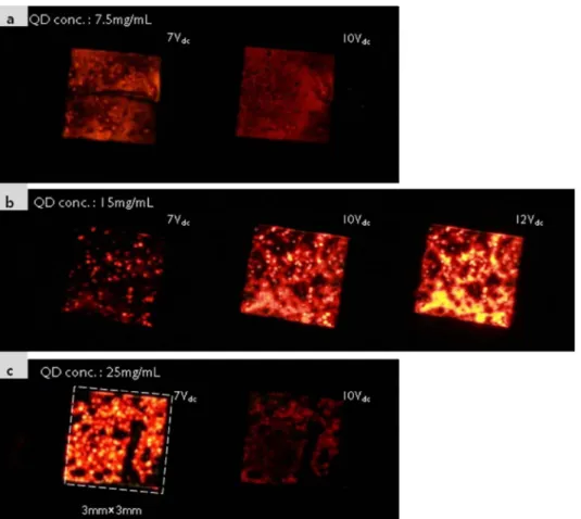
금속 산화물 반도체 전하 이동 층 표면 위에 형성된 양자점 분산액의 농도 변화에 따른 EL 특성의 변화를 Fig. 5 에 종합하였다. 톨루엔 용매로 희석하여 7.5, 15.0, 25.0 mg/mL 의 농도로 조절하였다.
Fig. 3. (color online) Photoluminescence showing the optical geo- metry of CdSe/ZnS QD layers coated with spin speed of 500 rpm on glass.
Fig. 2. Transmission electron microscope(TEM) image of the CdSe/ZnS quantum dots(QDs) demonstrating a 6 nm diameter.
Fig. 4. (color online) Electroluminescence at 10 V of QD-LED as a function of spin speed of (a) 1200, (b) 800 and (c) 500 rpm.
양자점의 농도가 7.5 mg/mL인 Fig. 5(a)의 경우, 직류 전압 7 V부터 전계발광이 시작되어 10 V 이상에서는 동
작하지 않았다. 양자점이 균일하게 도포되어 전면에 발광 특성이 나타난다. 이는 얇은 양자점 층이 EL 특성에 좋
Fig. 5. (color online) Electroluninescence at 7, 10, 12 V of QD-LED as a function of QD solution concentrations (a) 7.5 mg/mL, (b) 15.0 mg/mL and (c) 25.0 mg/mL of QD concentration.Fig. 6. (color online) AFM images of QDs layers on the ZTO film. QD concentrations are (a) 7.5 mg/mL, (b) 15.0 mg/mL and (c) 25.0 mg/mL.
지 않은 것으로 사료된다.
양자점의 농도가 15.0 mg/mL인 경우, Fig. 5(b)처럼 직 류 전압 7 V 인가에서 국부적으로 EL 특성이 구현되기 시작하여, 12 V에서 밝은 빛을 나타내었다. 최대 18 V까 지 밝기가 유지되다가 그 이상의 전압에서 동작이 멈추 었다. 국부적으로 발광이 일어나며, 비교적 넓은 전계 영 역에서 빛이 나오는 특성을 보인다.
양자점의 농도가 25.0 mg/mL인 경우, Fig. 5(c)처럼, 직류전압 7 V에서 동작하지만 10 V에서 동작을 멈추면 서 서서히 밝기가 줄어든다.
ZTO 층 위에 형성된 양자점 층의 표면 상태를 AFM 으로 관찰하면 Fig. 6과 같다. 농도 변화에 관계 없이 도포된 QD 층이 용액의 표면장력으로 국부적으로 모여 서 QD 층을 형성한 형태이다. 이러한 양자점 도포 상 태에서는 국부적으로 빛이 나오게 된다.
양자점의 농도가 7.5 mg/mL일 때는 Fig. 6(a)처럼 표 면 상태가 전체적으로 균일하게 도포된 것으로 사료된 다. 양자점의 농도가 15.0 mg/mL와 25.0 mg/mL일 때의 표면 상태는 Fig. 6(b,c)처럼 밝은 부분과 어두운 부분 으로 관찰되며, 이는 양자점이 국부적으로 응집된 것으 로 사료된다. 10 µm 크기로 응집된 양자점 코팅 층에 전 계를 가하면, Fig. 5처럼 점광원이 모여 면광원 형태를 보이는 것으로 사료된다.
4.
결 론금속산화물 전하 수송 층을 이용한 양자점 발광소자에 서 양자점 형성 스핀 속도와 양자점 분산액의 농도에 따 라 형성된 양자점의 배열과 상태가 변한다. 500 rpm 스 핀속도에서 형성한 양자점 코팅 층의 평활도가 우수하 였다.
양자점의 농도가 7.5 mg/mL일 때 얇은 층으로 도포되
어 EL 특성이 약하나, 양자점 분산액의 농도가 15.0 mg/
mL 일 때와 25.0 mg/mL일 때의 도포상태는 부분적으로 두꺼운 양자점 층이 형성되어 EL 특성이 나타나며, 이 러한 이유로 국부적 발광 특성이 개선되었다. EL 특성 개선을 위해, 하부 전하 이동층의 표면 거칠기 개선 및 표면 개질에 따른 스핀 코팅 특성 향상 연구 등, 균일 한 양자점 층 형성에 관한 추가 연구가 필요하다.
References
1. J. -M. Caruge, J. E. Halpert, V. Bulovic and M. G. Bawendi, Nano Lett., 6, 2991 (2006).
2. S. Coe, W. K. Woo, M. Bawendi and V. Bulovic, Nature 420, 800 (2002).
3. S. Coe-Sullivan, J. S. Steckel, W. K. Woo, M. G. Bawendi and V. Bulovic, Adv. Funct. Mater., 15, 1117 (2005).
4. P. O. Anikeeva, C. F. Madigan, J. E. Halpert, M. G.
Bawendi and V. Bulovic, Phys. Rev. B, 78, 085434 (2008).
5. M. Schlamp, X. Peng and A. P. Alivisatos, J. Appl.
Phys., 82, 5837 (1997).
6. J. Zhao, J. A. Bardecker, A. M. Munro and D. S. Ginger.
Nano Lett., 6, 463 (2006).
7. P. O. Anikeeva, J. E. Halpert, M. G. Bawendi and V.
Bulovic, Nano Lett., 9, 2532 (2009).
8. L. A. Kim, P. O. Anikeeva, S. Coe-Sullivan, J. S. Steckel, M. G. Bawendi and V. Bulovic, Nano Lett., 8, 4513 (2008).
9. J. -M. Caruge, J. E. Halpert, V. Wood, M. G. Bawendi and V. Bulovic, Nat. Photonics, 2, 247 (2008).
10. V. Wood, M. J. Panzer, J. -M. Caruge, J. E. Halpert, M.
G. Bawendi and V. Bulovic, Nano Lett., 10, 24 (2010).
11. V. I. Klimov, A. A. Mikhailovsky, Su Xu, A. J. Malko, A. Hollingsworth, C. A. Leatherdale, H. -J. M. Eisler and M. G. Bawendi, Science, 290, 314 (2000).
12. M. Maillard, L. Motte and M. -P. Pileni, Adv. Mater., 13, 200 (2001).