한국표면공학회지 J. Kor. Inst. Surf. Eng.
Vol. 47, No. 1, 2014.
http://dx.doi.org/10.5695/JKISE.2014.47.1.020
<연구논문>
Crystallization of Amorphous Silicon Films Using Joule Heating
Jae-Sang Ro
*Department of Materials Science and Engineering, Hongik University, Seoul 121-791, Korea
(Received February 6, 2014 ; revised February 19, 2014 ; accepted February 22, 2014)
Abstract
Joule heat is generated by applying an electric filed to a conductive layer located beneath or above the amorphous silicon film, and is used to raise the temperature of the silicon film to crystallization temperature.
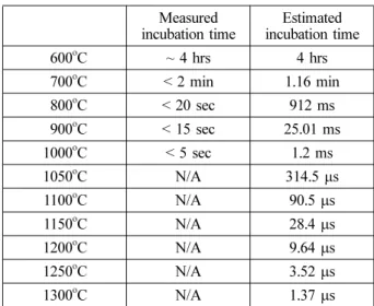
An electric field was applied to an indium tin oxide (ITO) conductive layer to induce Joule heating in order to carry out the crystallization of amorphous silicon. Polycrystalline silicon was produced within the range of a millisecond. To investigate the kinetics of Joule-heating induced crystallization (JIC) solid phase crys- tallization was conducted using amorphous silicon films deposited by plasma enhanced chemical vapor dep- osition and using tube furnace in nitrogen ambient. Microscopic and macroscopic uniformity of crystallinity of JIC poly-Si was measured to have better uniformity compared to that of poly-Si produced by other methods such as metal induced crystallization and Excimer laser crystallization.
Keywords : Crystallization, Poly-Si, AMOLED, Joule heating
1. Introduction
Active matrix organic light emitting diode (AMOLED) has recently come into the spotlight for its appli- cability to the next-generation flat panel displays. Since the device operates in a current-driven mode uniform source/drain current is critical for uniform picture quality. Low temperature polycrystalline silicon is thus preferred to a-Si for the thin-film-transistor backplanes.
A crystallization technology should produce poly-Si having a uniform grain size over the whole panel especially for AMOLED application. The methods of forming polycrystalline silicon at a low temperature include solid phase crystallization (SPC)
1), metal induced crystallization (MIC)
2), metal induced lateral crystalli- zation (MILC)
3), and Excimer laser crystallization (ELC)
4).
Several attempts have been made to anneal silicon films by applying an electric field during the crys- tallization of amorphous silicon films. By applying an electric field during MILC, Jun et al. attempted to fabricate polycrystalline silicon thin film transistors using field-aided lateral crystallization
5). Electric field
enhanced silicide mediated crystallization has also been reported for low temperature crystallization
6,7). In such methods, an electric field is applied to an a- Si film which has an ultrathin Ni layer during the crystallization process. Sameshima et al. proposed a crystallization method with pulsed electrical current- induced heating of silicon films. In coincidence with the voltage pulse, samples were irradiated with a 28-ns pulsed XeCl excimer laser. The authors reported that the melt duration time of the silicon thin films could be controlled using electrical current intensity in order to obtain large crystalline grain growth
8,9). They also reported the rapid crystallization of silicon films using Joule heating of metal films
10). Rapid Joule heating at an intensity of about 1.0 MW/cm
2was demonstrated by allowing current to flow in chromium metal strips located above a-Si films. This particular method involved the achievement of crystallization by melting silicon films.
We previously reported a crystallization method named as Joule heating induced crystallization (JIC)
11). In this technique, Joule heat is generated by applying an electric filed to a conductive layer located beneath or above the amorphous silicon film, and is used to raise the temperature of the silicon film to crystallization
*