Effect of the Cu Bottom Layer on the Optical and Electrical Properties of In 2 O 3 /Cu Thin Films
Daeil Kim*
School of Materials Science and Engineering, University of Ulsan, Ulsan 680-749 (Received July 13, 2011, Revised August 29, 2011, Accepted September 16, 2011)
Indium oxide (In
2O
3) single layer and In
2O
3/copper (Cu) bi-layer films were prepared on glass substrates by RF and DC magnetron sputtering without intentional substrate heating.
In order to determine the effect of the Cu bottom layer on the optical, electrical and structural properties of In
2O
3films, 3-nm-thick Cu film was deposited on the glass substrate prior to deposition of the In
2O
3films. As-deposited In
2O
3films had an optical transmittance of 79% in the visible wavelength region and a sheet resistance of 2,300 Ω/□, while the In
2O
3/Cu film had optical and electrical properties that were influenced by the Cu bottom layer.
In
2O
3/Cu films had a lower sheet resistance of 110 Ω/□ and an optical transmittance of 71%. Based on the figure of merit, it can be concluded that the Cu bottom layer effectively increases the performance of In
2O
3films for use as transparent conducting oxides in flexible display applications.
Keywords : In
2O
3, Cu, Magnetron sputtering, Sheet resistance, Optical transmittance
I. Introduction
Sn-doped indium oxide (In
2O
3), specifically an ITO thin film, is a highly degenerated, wide-gap semi- conductor with good conductivity and high optical transmission across the visible spectrum. As a result, ITO films are used in many applications such as solar cells [1], light emitting electrochemical cells [2], and variant flat panel displays [3]. ITO films can be pre- pared with high reproducibility using methods in- cluding reactive evaporation, reactive DC or RF sput- tering [4], ion beam assist deposition [5], and chem- ical vapor deposition (CVD) [6]. Among these meth- ods, DC or RF magnetron sputtering are two of the most frequently used deposition methods in optoelec-
tronic device manufacturing [4].
In conventional sputtering processes, substrate temperatures as high as 300
oC are required for depo- sition and/or post-annealing to obtain high quality transparent conducting oxide (TCO) films with rea- sonably high conductivity (~2×10
-4Ωcm) and trans- mittance ( ≥80% in the visible region) [7]. However, for certain applications, such as flexible optoelec- tronic devices, high substrate temperatures or high post-deposition annealing temperatures are un- desirable due to the low thermal resistance of the polymer substrates.
One way to improve the optical and electrical
properties of the transparent conducting oxide (TCO)
films without substrate heating is to use TCO/metal/
Effect of the Cu Bottom Layer on the Optical and Electrical Properties of In
2O
3/Cu Thin Films
TCO structures that have lower resistivity than TCO single layer films of the same thickness [8]. Recently Y. Kim reported ITO/Au/ITO multilayer films that have higher performance than that of ITO single lay- er films [9]. In this study, transparent and conduct- ing In
2O
3/copper (Cu) bi-layered films were deposited on a glass substrate without intentional substrate heating by RF and DC magnetron sputtering, and the effect of the Cu bottom layer on the optical, electrical and structural properties of the In
2O
3films were considered.
II. Experiments
In
2O
3and Cu thin films were deposited on a glass (Corning 1737) substrate without substrate heating by RF and DC magnetron sputtering equipped with two cathodes. RF (13.56 MHz) and DC power were applied to the In
2O
3(purity; 99.9%) and Cu (purity; 99.9%) targets, respectively. During deposition, the sub- strate temperature was monitored using a K-type thermocouple directly in contact with the substrate surface and was maintained at 70
oC. Prior to deposi- tion, the chamber was evacuated to a pressure of 2.0×10
-4Pa. Sputtering was performed at 1×10
-1Pa in argon (Ar) and the deposition distance between the target and substrate was maintained at 7 cm. By con- trolling the deposition time and sputtering power, the film thickness for In
2O
3and Cu was maintained at 100 nm and 3 nm, respectively. For comparison, In
2O
3single layer films without a Cu bottom layer were also deposited under the same deposition conditions.
After deposition, film thickness was confirmed with a surface profilometer (Dektak 150, Veeco) and atomic force microscopy (AFM, XE-100, Park Systems). The crystallization of the films was ob- served with high resolution X-ray diffraction (XRD, X ’ pert Pro MRD, Philips) at the Korea Basic Science Institute (KBSI, Daegu Center). The surface rough-
ness was analyzed using AFM on 2×2 μm
2sample areas. In addition, optical and electrical properties were assessed using a four-point probe (MCP-T360, Mitsubishi), a Hall automatic measuring system (HMS-3000, Ecopia) and a UV-Vis. Spectrophoto- meter (Cary 100 Cone, Varian), respectively. The glass substrates showed a 92% optical transmittance in the visible wavelength range. The performance of the In
2O
3and In
2O
3/Cu films as transparent conduct- ing films was evaluated using the figure of merit (FOM) [10].
III. Results and Discussion
In XRD measurements, none of the films showed diffraction peaks in the patterns, indicating that they were all amorphous and the low substrate temperature prohibited crystallization. In a previous study, Kim reported that the Au bottom layer in ITO/Au bi-lay- ered films promotes the crystallization of the upper ITO film without intentional substrate heating [11] or a post-deposition annealing process [12]. However, the Cu bottom layer in the present study did not effec- tively crystallize the upper In
2O
3film.
Fig. 1 shows the three-dimensional AFM images of as-deposited Cu, In
2O
3and In
2O
3/Cu films. The root mean square (RMS) roughness of the as-deposited Cu and In
2O
3films was 0.3 and 1.1 nm, respectively, while the RMS roughness of the In
2O
3/Cu bi-layered films was 6.4 nm.
As shown in Fig. 1, though the thin Cu bottom lay- er had a flat surface morphology, it increased the surface roughness of the upper In
2O
3film effectively in the bi-layered films. Since the rough surface mor- phology resulted in a wider film surface area, it can be inferred that the effect of the Cu bottom layer on the surface roughness is favorable for solar cells and gas sensor applications of In
2O
3films.
Fig. 2(a) shows the optical transmittance in a
Figure 1. The three-dimensional AFM images of as- deposited Cu, In
2O
3and In
2O
3/Cu films. (a) Cu thin film, (b) In
2O
3film, (c) In
2O
3/Cu film.
Figure 2. (a) Optical transmittance of In
2O
3and In
2O
3/ Cu films, (b) Optical absorption of In
2O
3and In
2O
3/Cu films.
Figure 3. A parallel electrical resistance circuit model of In
2O
3/Cu bi-layer films.
wavelength range of 300 ∼900 nm. The In
2O
3and In
2O
3/Cu films had optical transmittances (with a glass substrate) in the visible wavelength region of 79% and 71%, respectively. Fig. 2(b) shows the optical absorption in the wavelength range of 300 ∼900 nm.
The In
2O
3/Cu films had greater absorption than that of the In
2O
3single layer films.
The optical absorption at the interface between the In
2O
3and Cu films reduced the optical transmittance of the In
2O
3/Cu films. In addition, the rougher In
2O
3/Cu surface increased the absorption of the in- cident light and may also have reduced the optical transmittance.
Along with the optical analysis, the electrical properties of the films were evaluated. Fig. 3 shows a parallel electrical resistance circuit model of the In
2O
3/Cu bi-layer films. Based on the amount of flowing electrical current, the bottom Cu layer had a thickness of 3 nm and a sheet resistance of 3.56×10
6Ω/□. The electrical resistance can be calculated
with the simple equation:
1 / R
Total= 1 / R
Cu+ 1 / R
In2O3,where R
Total, R
Cuand R
In2O3refer to the total resist- ance, the resistance of the Cu bottom layer and the resistance of the In
2O
3upper layer in the In
2O
3/Cu films, respectively. The relationship between resist- ance (R) and resistivity (ρ) is expressed as R = (ρl)/A, where l is the length and A is the cross-sectional area.
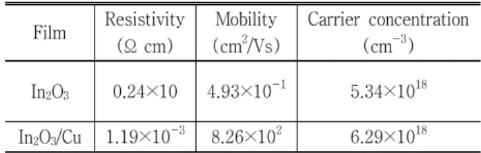
Table 1 shows the electrical properties of In
2O
3and
Effect of the Cu Bottom Layer on the Optical and Electrical Properties of In
2O
3/Cu Thin Films
Table 1. The electrical properties of In
2O
3and In
2O
3/ Cu bi-layered films.
Film Resistivity (Ω cm)
Mobility (cm
2/Vs)
Carrier concentration (cm
-3) In
2O
30.24×10 4.93×10
-15.34×10
18In
2O
3/Cu 1.19×10
-38.26×10
26.29×10
18Table 2. Comparison of optical, electrical properties and figure of merit (FOM, Ω
-1) of In
2O
3and In
2O
3/Cu bi-layered films.
Properties In
2O
3/Cu In
2O
3Optical transmittance (%) 71 79 Sheet resistance (Ω/ ⃞) 110 2,300 Figure of merit (Ω
-1) 2.9×10
-44.1×10
-5In
2O
3/Cu film and the In
2O
3/Cu bi-layered Film shows the lower resistivity than that of the In
2O
3films.
Table 2 shows the optical and electrical properties of the films. The In
2O
3/Cu films had a lower sheet re- sistance than that of the In
2O
3single layer films. The figure of merit (FOM) is an important index for eval- uating the performance of transparent conducting oxide (TCO) films [13]. The FOM is defined as FOM=
T
10/R
s, where T is the optical transmittance and R
sis the sheet resistance. The FOM reached a maximum of 2.9×10
-4Ω
-1for the In
2O
3/Cu layered films, which is greater than the FOM for the In
2O
3single layer films prepared in this study, which was 4.1×10
-5Ω
-1.
As higher FOM indicates better quality TCO films, the In
2O
3/Cu layered films will likely perform better in TCO applications than In
2O
3single layer films.
IV. Conclusions
Both In
2O
3and In
2O
3/Cu bi-layered films were de- posited without intentional substrate heating on glass substrates using RF and DC magnetron sputtering. In this study, the optical and electrical properties were
highly dependent on the Cu bottom layer in the In
2O
3/Cu films. A TCO that had a sheet resistance of 110 Ω/ ⃞ and a high optical transmittance of 71% in the visible wavelength region was obtained from the 100 nm In
2O
3/3 nm Cu films.
Figure of merit for the In
2O
3/Cu films reached a maximum value of 2.7×10
-4Ω
-1, which was greater than that of the In
2O
3single layer films. This result indicates that the 3-nm-thick Cu bottom layer in the In
2O
3/Cu films results in better performance than conventional In
2O
3single layer films.
References
[1] H. Yano, D. Kouro, N. Sasaki, and S. Muramatsu, Sol. Ener. Mater. Sol. Cells 93, 976 (2009).
[2] Z. You and J. Dong, Microelectron J. 38, 108 (2007).
[3] U. Betz, M. Olsson, J. Martly, and M. Escola, Surf.
Coat. Technol. 200, 5751 (2006).
[4] M. H. Ahn, E. S. Cho, and S. J. Kwon, J. Korean Vaccum Soc. 18, 440 (2009).
[5] J. H. Song, D. K. Choi, and W. K. Choi, J. Korean Vaccum Soc. 1, 55 (2003).
[6] K. Maki, N. Komiya, and A. Suzuki, Thin Solid Films 445, 224 (2003).
[7] D. Kim, D. Ma, and N. Lee, Jpn. J. Appl. Phys.
43, 1536 (2004).
[8] J. Park, J. Chae, and D. Kim, J. Alloy. Comp. 478, 330 (2009).
[9] Y. Kim, J. Park, D. Choi, H. Jang, J. Lee, H. Park, J. Choi, D. Ju, J. Lee, and D. Kim, Appl. Surf. Sci.
254, 1524 (2007).
[10] G. Haacke, J. Appl. Phys. 47, 4086 (1976).
[11] Y. Kim, J. Park, and D. Kim, Vacuum 82, 574 (2008).
[12] D. Kim, Appl. Surf. Sci. 256, 1774 (2010).
[13] D. Kim, Displays 31, 155 (2010).
구리 기저 층이 In 2 O 3 /Cu 박막의 광학적, 전기적 특성에 미치는 영향
김대일*