DOI: http://dx.doi.org/10.4313/JKEM.2012.25.7.491
다양한 버퍼층 위에 증착한 In 2 O 3 박막의 구조, 광학 및 전기적 특성
김문환1,a
1 신라대학교 자동차기계공학과
Structural, Optical, and Electrical Properties of In 2 O 3 Thin Films Deposited on Various Buffer Layers
Moonhwan Kim
1,a1 Department of Automotive and Mechanical Engineering, Silla University, Busan 617-736, Korea
(Received April 30, 2012; Revised June 20, 2012; Accepted June 21, 2012)
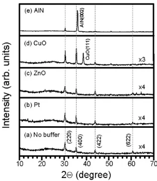
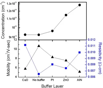
Abstract: The effects of various buffer layers on the In2O3 transparent conducting films grown on glass substrates by radio-frequency reactive magnetron sputtering were investigated. The In2O3 thin films were deposited at 400℃ of growth temperature and 100% of oxygen flow rate. The optical, electrical, and structural and morphological properties of the In2O3 thin films subjected to buffer layers were examined by using ultraviolet-visible spectrophotometer, Hall-effect measurements, and X-ray diffractometer, respectively. The properties of In2O3 thin films showed different results, depending on the type of buffer layer. As for the In2O3 thin film deposited on ZnO buffer layer, the average transmittance was 89% and the electrical resistivity was 7.4×10⁻³ Ωcm. The experimental results provide a way for growing the transparent conducting film with the optimum condition by using an appropriate buffer layer.
Keywords: Buffer layer, In2O3 thin film, Magnetron sputtering