Current Photovoltaic Research 4(1) 12-15 (2016)
DOI:http://dx.doi.org/10.21218/CPR.2016.4.1.012 pISSN 2288-3274
Investigation of Firing Conditions for Optimizing
Aluminum-Doped p + -layer of Crystalline Silicon Solar Cells
Sang Hee Lee ․ Doo Won Lee ․ Eun Gu Shin ․ Soo Hong Lee*
Green Strategic Energy Research Institute, Department of Electronics Engineering, Sejong University, Seoul, Korea
ABSTRACT: Screen printing technique followed by firing has commonly been used as metallization for both laboratory and industrial based solar cells. In the solar cell industry, the firing process is usually conducted in a belt furnace and needs to be optimized for fabricating high efficiency solar cells. The printed-Al layer on the silicon is rapidly heated at over 800°C which forms a layer of back surface field (BSF) between Si-Al interfaces. The BSF layer forms p-p
+structure on the rear side of cells and lower rear surface recombination velocity (SRV). To have low SRV, deep p
+layer and uniform junction formation are required. In this experiment, firing process was carried out by using conventional tube furnace with N
2gas atmosphere to optimize V
ocof laboratory cells. To measure the thickness of BSF layer, selective etching was conducted by using a solution composed of hydrogen fluoride, nitric acid and acetic acid. The V
ocand pseudo efficiency were measured by Suns-V
octo compare cell properties with varied firing condition.
Key words: Aluminum, Back surface field, Firing process, Tube furnace, Suns-V
oc*Corresponding author: [email protected]
Received February 23, 2016; Revised February 27, 2016;
Accepted February 29, 2016
ⓒ 2016 by Korea Photovoltaic Society
This is an Open Access article distributed under the terms of the Creative Commons Attribution Non-Commercial License (http://creativecommons.org/licenses/by-nc/3.0)
which permits unrestricted non-commercial use, distribution, and reproduction in any medium, provided the original work is properly cited.
1. Introduction
In the crystalline silicon solar cell industry, the screen printed method has widely been used to form front and back metallization since it is a rapid and cost effective process compared to other methods. Even though the method is a conventional technique in the industry, it still needs optimization for high efficiency solar cells. There are many research trends to improve efficiency of solar cells such as screen printed finger width, paste contents, firing temperatures, thickness, paste viscosity etc.
1). Particularly, firing temperature is one of the important factors for determining characteristics of the solar cell. In case of front metallization using screen printing method, the over-fired front contact has an effect that creates a shunting path which is critical for fill factor of solar cell by crystallite through emitter
2). On the other hand, less-fired front contact occurs in high contact resistance due to insufficient contact formation
3). Moreover, this firing process is also important to back side metallization using screen printing.
After firing process on back side metallization, BSF is formed between crystalline silicon wafer and Al back contact. The BSF is highly Al doped Si layer, and the layer acts as a p
+layer.
Therefore, the solar cell which is made by p-type crystalline
silicon wafer has an n
+-p-p
+junction
1,3). This p-p
+region forms an electric field and creates a barrier to minority carrier flow to rear side. The BSF layer thus has an effect that minimizes the rear surface recombination velocity. Moreover, BSF has a net effect of passivation of the rear surface
4-6). Therefore, the BSF layer thickness control and uniformity are majorly focused since solar cell characteristics are varied by these factors
7,8). BSF layer thickness is normally followed by quantity of dissolved Si onto Al-Si melted layer at peak temperature
1,8). The uniformity of BSF layer is also related to the firing peak temperature. Thus in this paper, BSF uniformity and layer thickness are analyzed for dependence upon firing process time and peak temperature.
2. Experimental
2.1 Dependence of process time on BSF thickness Samples were prepared with (100) Czochralski (CZ) p-type wafers to study the influence of process time which was divided to input time and sintering time at the center of a furnace. Al paste was screen printed on the wafers with 30µm of thickness.
The printed-Al paste was dried at 285°C for 2 minutes by using a hot plate. The firing process for forming BSF layer was conducted in a 3-zone conventional tube furnace (Fig. 1) with N
2gas atmosphere.
The Al firing temperature was fixed at 840°C, as a typical
12
S.H. Lee et al. / Current Photovoltaic Research 4(1) 12-15 (2016) 13
Fig. 1. Schematic view of the firing process in the tube furnace
Table 1. Varied Al firing duration on each step; input and sintering at the center
Temp. Time at the
front Input Time at the
center Output
840°C 20 sec
10 sec
40 sec
10 sec 20 sec
40 sec No stay
20 sec
Table 2. Varied Al firing temperature with the fixed process duration
Temp. Time at the
front Input Time at the center Output 820°C
20 sec 40 sec 20 sec 10 sec
840°C 860°C
Fig. 2. Schematic structure and feature of completed cell
range of 800~900°C is usually considered for Al firing. The samples were kept at the mouth of the furnace for 20 seconds to volatilize the residue of paste solvents. The duration of input and sintering at the center of furnace were varied as Table 1 summarizes. The sample take off time from the center to the mouth was kept constant at 10 seconds.
To etch the BSF layer selectively, samples were dipped in a solution which was composed of hydrogen fluoride (HF), nitric acid (HNO
3), and acetic acid (CH
3COOH). Thickness of the BSF layer was measured by using FE-SEM.
2.2 V
ocoptimization with varied firing temperature Mini-cells of 2x2 cm
2size were fabricated with half cells to compare V
ocaccording to the different firing temperatures. The half cells which were produced by E&R Solar (Kyengbuk, Korea) had an emitter of 72 ohm/sq sheet resistance and were deposited with SiN
x:H as an anti-reflection coating (ARC) and passivation layer. The SiN
x:H layer on the wafer was opened by using photolithography for the front grid area. Afterwards, Al paste was screen printed and fired at different temperatures with the fixed process time as Table 2 shows. As a front contact, Ni/Cu/Ag plated contact was used. On the laser ablated area, nickel was deposited by using an electroless plating, then Cu/Ag main metal stacks were plated by using a light induced plating (LIP) for uniform metal thickness. The completed cell structure and feature are schematized in Fig. 2
The cells were measured by Suns-V
oc(Sinton Instruments, USA) to compare V
ocand pseudo efficiency (pEffi). Also, BSF
layer thickness of the cells was compared with the same methods as explained in section 2.1.
3. Result and Discussion
3.1 Dependence of process time on BSF thickness Before we optimized the firing temperature, we investigated the thickness of BSF by changing process duration. Fig. 3 shows the FE-SEM cross section image of samples with different input time and fixed time of sintering at the center of the furnace.
Measured BSF thickness of each condition was 7.5 µm and 4.5 µm for 20 sec and 10 sec of input time, respectively. The BSF was thicker for the longer input time since duration at peak temperature (t
peak) was increased. If t
peakis increased, more silicon can be dissolved into the Si-Al melt and epitaxially recrystallized when the sample is cooled down
9-11).
We also changed sintering time at center of the furnace with fixed input time to 40 sec. As Fig. 4 shows the thickness of the BSF layer, sample with longer time (20 sec) of sintering at the center had about 1 µm thicker layer (5.8 µm) compared to the sample which was directly taken out from the center. Even though the BSF thickness was influenced by the longer sintering time at the center, which increased the t
peak, the thickness difference was larger with the increased input time.
By varying the process time, we obtained the BSF thickness
from 4.5~7.5 µm. Although the thicker BSF layer can reduce the
back surface recombination velocity, it can also reduce absorb
layer of the wafer. In the next chapter, we evaluate V
ocwith
different firing temperature to optimize the BSF forming condition.
S.H. Lee et al. / Current Photovoltaic Research 4(1) 12-15 (2016) 14
Fig. 3. FE-SEM cross sectional image of the samples with different input time into the furnace; (a) 20 sec and (b) 10 sec
Fig. 4. FE-SEM cross sectional image of the samples with different sintering time at center of the furnace; (a) no stay and (b) 20 sec
Fig. 5. The error bar graph of (a) Voc and (b) pEffi values
Fig. 6. (a) the error bar graph of BSF thickness for the different firing temperature. (b) FE-SEM cross section of the sample which was fired at 860°C
3.2 V
ocoptimization with varied firing temperature The BSF quality and uniformity of cells at different firing temperature were evaluated by comparing V
oc. The V
ocof cells were measured by Suns-V
ocwhich can measure V
ocwith varied light intensity. The V
ocvalue from the Sun-V
oconly can be different with the actual value when temperature is changed.
The measurement details are well explained by R. A. Sinton and A. Cuevas
12). The error bar graphs in Fig. 5 show average V
ocand pEffi values of three cells for different firing temperature. The lowest V
ocof 618 mV was measured at 820°C. At 840°C, the maximum and average value of V
ocwas increased and recorded the highest value of 624 mV. However, average V
ocwas decreased to 621 mV at 860°C. The aspect of V
ocwas matched well with pEffi results which was recorded at 19.2% as the highest value.
V
ocof solar cells is affected by uniformity of BSF layer.
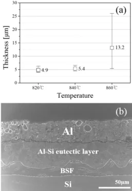
When the peak Al-Si alloying temperature exceeds a critical value, Al surface reveals a lot of bumps and BSF layer becomes non-uniform
1). As Fig. 6(a) shows the error bar graph of the BSF thickness, the deviation of thickness at 860°C was from 5 to 26 µm which was extremely higher than other conditions. Also, Al-Si eutectic layer which is located between Al and BSF layer had large difference of thickness depending on area. In the area of bumps, eutectic layer thickness was around 50 µm (Fig. 6(b)) while other areas had 2~5 µm. Due to the eutectic layer having strong relation of lateral conductivity of the rear contact, inhomogeneous eutectic layer thickness will adversely influence
on the cell performance
10).
To optimize the process of Al rear contact formation, printed-
Al thickness also can be controlled. When Al thickness becomes
thin, peak temperature of firing without agglomeration is increased
S.H. Lee et al. / Current Photovoltaic Research 4(1) 12-15 (2016) 15
exponentially
1). Although the value of Al thickness and peak temperature was not exactly matched with our results, we could find optimal temperature with 30 µm Al layer. In this experiment, we optimized V
ocat 840°C. However, we can also decrease Al thickness for using higher peak temperature and BSF thickness can be thicker (~10 µm) for further reducing surface recombination velocity
13).
4. Conclusions
To investigate proper thickness of BSF layer and optimize V
ocof laboratory cells, the firing process time and peak temperature in tube furnace were varied. The increase of BSF thickness was more prominent for the varied input duration than sintering time at the center of the furnace. Also, 2x2 cm
2size cells which had Ni/Cu/Ag plated front contact was measured by Suns-V
octo compare the V
ocand pEffi. The V
ocand pEffi recorded peak value (624 mV, 19.2%) at 840°C with 30 µm Al thickness. At higher temperature (860°C), agglomeration was occurred and disturbed uniform BSF layer formation.
Acknowledgments
This work was supported by the New & Renewable Energy Core Technology Program of the Korea Institute of Energy Technology Evaluation and Planning (KETEP) granted by financial resource from the Ministry of Trade, Industry & Energy, Republic of Korea (No. 20133010011780).
References
1. Meemongkolkiat V, Nakayashiki K, Kim DS, Kopecek R, Rohatgi A, “Factors limiting the formation of uniform and thick aluminum back-surface field and its potential”, Journal of the Electrochemical Society, Vol. 153, Issue 1, 2006, pages G53-G58.
2. Hilali MM, Nakayashiki K, Khadilkar C, Reedy RC, Rohatgi A, Shaikh A, et al., “Effect of Ag particle size in thick-film Ag paste on the electrical and physical properties of screen printed
contacts and silicon solar cells”, Journal of the Electrochemical Society, Vol. 153, Issue 1, 2006, pages A5-A11.
3. Gatz S, Hannebauer H, Hesse R, Werner F, Schmidt A, Dullweber T, et al., “19.4%‐efficient large‐area fully screen‐printed silicon solar cells”, physica status solidi (RRL)-Rapid Research Letters, Vol. 5, Issue 4, 2011, pages 147-149.
4. Loelgen P, Leguijt C, Eikelboom J, Steeman R, Sinke W, Verhoef L, et al., editors, “Aluminium back-surface field dop- ing profiles with surface recombination velocities below 200 cm/s”, IEEE Photovoltaic Specialists Conference, 1993.
5. Rauer M, Woehl R, Rühle K, Schmiga C, Hermle M, Hörteis M, et al., “Aluminum alloying in local contact areas on dielec- trically passivated rear surfaces of silicon solar cells”, IEEE Electron Device Letters, Vol. 32, Issue 7, 2011, pages 916-918.
6. Gatz S, Bothe K, Müller J, Dullweber T, Brendel R, “Analysis of local Al-doped back surface fields for high efficiency screen- printed solar cells”, Energy Procedia, Vol. 8, 2011, pages 318-323.
7. Rohatgi A, Narasimha S, Ebong AU, Doshi P, “Understanding and implementation of rapid thermal technologies for high-effi- ciency silicon solar cells”, IEEE Transactions on Electron Devices, Vol. 46, Issue 10, 1999, pages 1970-1977.
8. Narasimha S, Rohatgi A, Weeber A, “An optimized rapid alu- minum back surface field technique for silicon solar cells”, IEEE Transactions on Electron Devices, Vol. 46, Issue 7, 1999, pages 1363-1370.
9. Rauer M, Schmiga C, Hermle M, Glunz SW, “Effectively sur- face‐passivated aluminium‐doped p+ emitters for n‐type silicon solar cells”, physica status solidi (a), Vol. 207, Issue 5, 2010, pa- ges 1249-1251.
10. Rauer M, Schmiga C, Krause J, Woehl R, Hermle M, Glunz SW, “Further analysis of aluminum alloying for the formation of p+ regions in silicon solar cells”, Energy Procedia, Vol. 8, 2011, pages 200-206.
11. Krause J, Woehl R, Rauer M, Schmiga C, Wilde J, Biro D,
“Microstructural and electrical properties of different-sized alu- minum-alloyed contacts and their layer system on silicon surfa- ces”, Solar Energy Materials and Solar Cells, Vol. 95, Issue 8, pages 2151-2160.
12. Sinton R, Cuevas A, editors, “A quasi-steady-state open-circuit voltage method for solar cell characterization”, 16th European Photovoltaic Solar Energy Conference, 2000.
13. Park SE, “A study on interfacial reaction in aluminum metal- lization process for crystalline silicon solar cells”, Dessertation Thesis, Korea University, Korea, 2012.