1. 서 론
P-type 결정질 실리콘 웨이퍼를 이용하여 제작하는 태양전지는 현재까지도 태양광 발전 분야에서 높은 점
a. Corresponding author; [email protected] Copyright ©2017 KIEEME. All rights reserved.
This is an Open-Access article distributed under the terms of the Creative Commons Attribution Non-Commercial License (http://creativecommons.org/licenses/by-nc/3.0) which permits unrestricted non-commercial use, distribution, and reproduction in any medium, provided the original work is properly cited.
유율을 차지하고 있다. 하지만 P-type 웨이퍼에 존재 하는 최대 1×10¹⁸개의 oxygen이 boron dopant와 결 합하여 boron-oxygen complex를 형성하게 되고, 이 는 light-induced degradation (LID)을 야기하게 되 어 minority carrier life time (MCLT)의 감소와 더 불어 모듈에서는 1~3%의 효율 감소를 보이며 태양전지 에서는 0.2~0.5% 효율을 저하시키는 원인이 된다 [1,2].
그러나 N-type 태양전지의 경우 기판에 phosphorus 가 존재하기 때문에 B-O complex에 의한 LID 현상이
N-type 고효율 태양전지용 Boron Diffused Layer의 형성 방법 및 특성 분석
심경배1, 박철민2, 이준신1,a
1 성균관대학교 정보통신대학
2 성균관대학교 에너지과학과
Boron Diffused Layer Formation Process and Characteristics for High Efficiency N-type Crystalline Silicon Solar Cell Applications
Gyeongbae Shim
1, Cheolmin Park
2, and Junsin Yi
1,a1 College of Information and Communication Engineering, Sungkyunkwan University, Suwon 16419, Korea
2 Department of Energy Science, Sungkyunkwan University, Suwon 16419, Korea
(Received October 27, 2016; Accepted February 3, 2017)
Abstract: N-type crystalline silicon solar cells have high metal impurity tolerance and higher minority carrier lifetime that increases conversion efficiency. However, junction quality between the boron diffused layer and the n-type substrate is more important for increased efficiency. In this paper, the current status and prospects for boron diffused layers in N-type crystalline silicon solar cell applications are described. Boron diffused layer formation methods (thermal diffusion and co-diffusion using a-SiOX:B), boron rich layer (BRL) and boron silicate glass (BSG) reactions, and analysis of the effects to improve junction characteristics are discussed. In-situ oxidation is performed to remove the boron rich layer. The oxidation process after diffusion shows a lower B-O peak than before the Oxidation process was changed into SiO2 phase by FTIR and BRL. The a-SiOX:B layer is deposited by PECVD using SiH4, B2H6, H2, CO2 gases in N-type wafer and annealed by thermal tube furnace for performing the P+
layer. MCLT (minority carrier lifetime) is improved by increasing SiH4 and B2H6. When a-SiOX:B is removed, the Si-O peak decreases and the B-H peak declines a little, but MCLT is improved by hydrogen passivated inactive boron atoms. In this paper, we focused on the boron emitter for N-type crystalline solar cells.
Keywords: N-type c-Si solar cell, Boron diffusion, Co-diffusion
ISSN 1226-7945(Print), 2288-3258(Online)
생기지 않을 뿐만 아니라 Fe에 의한 불안정성이 없어 높은 lifetime을 가지고 있다 [3]. 이처럼 우수한 웨이퍼 품질과 inactive doping의 차이에 의한 boron diffusion layer의 낮은 saturation current density (J0e)는 N-type 태양전지의 장점이다 [4]. 하지만 이러한 장점에도 불구하고 boron diffusion layer의 형성, passivation에 연관된 기술적 도전과 비용 때문에 P-type 실리콘 태양전지가 주류를 이루고 있으며 다양 한 boron diffusion 기술들이 현재까지 조사 및 사용 되고 있지만 뚜렷하게 우위에 있는 기술은 나오고 있 지 않은 상황이다 [5].
N-type 웨이퍼에 Boron 확산은 고체 source (B2O3, BN), 액체 source [BBr3, (CH3O)3B), 기체 source (B2H6, BF3, BCl3)을 이용하여 thermal furnace, spin on doping, ion implantation 등 다양한 기술과 공정 방법이 연구 및 사용되고 있다.
다양한 diffusion 방법 중에서, 액체 소스는 대표적 으로 BBr3와 BCl3를 source로 사용하며 표면 농도의 균일성이 우수하고 반송가스의 유입과 차단을 통해 확 산 공정의 시작과 종결을 쉽게 조절할 수 있는 장점이 있다. 또한 액체 소스를 사용한 확산 공정 시 생기는 Br2와 Cl2와 같은 부산물들은 중금속 gettering 효과를 볼 수 있어서 효율 향상에도 도움이 된다 [4].
Boron diffused layer에서 가장 문제시 되는 부분 이 BRL (boron rich layer)의 제어이다. BRL은 BSG 와 P+ layer 사이에 존재하며 두께는 대략 5~300 nm 로 형성된다. Boron diffusion시 산소와 질소 그리고 BBr3는 아래와 같은 과정을 거쳐 반응을 한다.
4BBr3 (g) + 3O2 (g) → 2B2O3 (l) + 6Br2 (g) (1) 2B2O3 (l) + 3Si (s) → 4B (s) + 3SiO2 (s) (2)
위 반응에서 남은 SiO2는 부분적으로 액체 상태인 B2O3에 용해되어 B2O3-SiO2 system인 BSG를 생성하 게 된다. 이 과정에서 고농도 boron 원소가 웨이퍼 표 면에 존재하게 되는데 이때 확산하지 못한 boron 원 소들이 표면 실리콘 원소와 결합하여 Si-B (boron rich layer)가 아래의 반응식과 같이 생성이 된다 [6].
Si + 6B → SiB6 (3)
이러한 BRL은 캐리어의 전자와 정공의 재결합 사이 트로 작용하며 BRL의 증가는 bulk lifetime을 감소시 키기 때문에 태양전지의 효율 향상을 위해서는 BRL의 제거는 필수이다 [7]. BSG는 HF로 제거 가능하지만 BRL은 HF용액 처리 후에도 제거되지 않고 웨이퍼 표 면에서 hydrophilic하게 남게 된다 [8]. BRL을 제거하 기 위해서는 in-situ oxidation, low temperature oxidation (LTO) 그리고 용액 에칭 등 여러 가지 방법 들이 있다 [8,9].
최근 diffusion시의 공정비용 및 시간을 줄이기 위 해 CVD (chemical vapor deposition)을 이용한 co-diffusion 방법이 연구 및 적용되고 있다. 주로 a-SiOX:B (boron doped amorphous silicon oxide) layer를 소스로 이용하여 boron을 확산 시키는데, N-type 웨이퍼에 a-SiOX:B를 APCVD (atmosphere pressure chemical vapor deposition) 또는 PECVD (plasma enhanced CVD) 장비를 이용하여 증착한 후, furnace를 이용하여 p+ layer를 형성 시킨다. 이 러한 방법은 co-diffusion을 통해 p+와 n+ layer를 동시에 형성 할 수 있게 하여 공정 시간을 단축시켜 throughput의 향상과 thermal stress를 감소를 통한 효율 향상을 기대할 수 있다 [10-12].
2. 실험 방법
BRL (boron rich layer)을 제거하기 위해 in-situ oxidation을 진행하였다. 기본 도핑 공정은 BBr3
source를 이용하여 furnace에서 진행되며 950℃에서 pre-deposition이 15분, 1,050℃에서 drive-in이 20 분 진행되어 면저항(RS) 45 Ω/sq를 가진다. oxidation 공정은 pre-deposition 후 950℃ 5분, drive-in 후 5 Fig. 1. Various diffusion process type for c-Si solar cell
fabrication.
분 두 조건에서 실험이 진행되었다.
a-SiOX:B layer를 N-type 웨이퍼에 증착을 위해 SiH4, B2H6, H2, CO2와 같은 가스를 사용하여 PECVD (plasma enhanced chemical vapor deposition)장 비로 증착하였다. 온도, 압력, plasma 파워를 조절하 여 증착을 시킨다. 증착 후 SiNX 또는 SiOX layer를 통해 capping을 하여 boron과 phosphorus cross doping을 방지하였다. tube furnace를 이용하여 N2
와 O2 가스 분위기에서 p+ layer를 형성시켰다.
P+ layer의 면저항을 측정하기 위해 4-point prove 를 이용하였으며 lifetime과 iVOC (implied Voc) 측정 을 위해 QSSPC (WCT-120)를 이용하였다. Oxygen annealing에 따른 bonding 구조의 확인을 위해 FTIR 측정을 수행하였다.
3. 결과 및 고찰
3.1 BRL / BSG 제거
BRL의 존재는 더 나은 균일한 면저항(RS) 확보에 밀 접한 관계를 가지고 있지만, 웨이퍼의 dislocation과 같 은 defect를 발생시키거나 bulk lifetime degradation 과 같은 문제를 발생시킨다. Kessler 연구팀들은 10 nm보다 더 두꺼운 두께를 가지고 있는 BRL의 경우 cooling down 구간에서의 열팽창계수에 의한 thermal stress를 일으켜 bulk lifetime의 감소를 일으킨다고 밝혔다. 또한, BRL의 존재는 고효율 N-type 태양전지 제작을 위해 필수적인 boron이 확산된 웨이퍼 표면의 높은 passivation효과에 악영향을 주기 때문에 제거되 어야 한다 [8,13].
그림 2에서 나타나는 것과 같이 B-O peak (1,300
~1,500 cm-1)을 관찰함으로써 BSG/BRL의 유무를 판 단하였다. 기본 조건의 FTIR 결과에서는 B-O bonding 이 남아 있으나, oxygen annealing에서는 B-O peak 가 줄어들어 B-O bonding에 의한 defect가 감소하여 BSG/BRL의 제거가 되었다고 판단할 수 있다. 또한, 전기 음성도 차이에 따라 oxygen anneal에 의해 주 입된 oxygen에 의해 Si-O bonding이 주도하게 되어 Boron 원자가 Si 내부로 확산되는 것으로 판단된다.
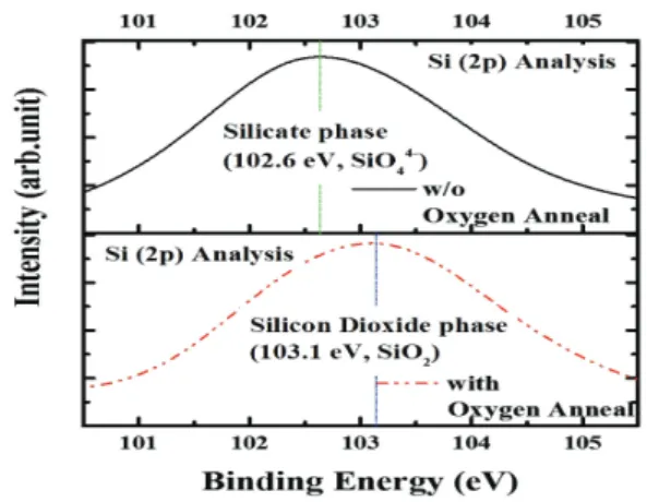
그림 4의 XPS 분석 결과에서와 같이 oxygen annealing을 적용하지 않은 경우, silicate phase (SiO44-)가 BSG를 주도하고 있으나, oxygen anneal을 적용한 결과의 분석 결과는 binding energy상에서 SiO2 phase로 BSG가 변한 것을 확인 할 수 있다. 이는 웨이퍼 표면에 잔재하는 BSG의 특성변화가 oxygen anneal에 의해 일어났음을 밝혀준다.
3.2 a-SiOX:B을 이용한 boron emitter 형성
N-type 실리콘 태양전지의 제작 시, 두 번의 확산 Fig. 2. After boron diffusion, variation of Si, B, O’s contents
according to O2 treatment.
Fig. 3. Silicon, oxygen and boron electro -negativity and bonding mechanism of diffusion process.
Fig. 4. XPS analysis of BSG layer by oxygen annealing process.
공정은 두 번의 thermal stress를 거치게 되어 태양전 지 성능저하에 원인이 될 뿐 아니라 공정 시간의 증가 로 인해 throughput 저하로 이어진다. 또한 J. Schon 연구팀들은 boron emitter와 phosphorus BSF 의 co-doping에 의해 impurity gettering이 증가하였다 고 보고하였다 [14,15].
표 1과 같이 SiH4를 두 개의 조건을 두고 세부 조건 으로 B2H6를 3가지의 조건으로 가변을 하였다. SiH4의 양이 증가할수록 전반적으로 면저항(RS)의 면저항(RS) 이 같은 annealing 조건에서 더 낮은 면저항(RS) 값이 나왔으며 더 높은 lifetime 값을 가졌다. B2H6의 flow 양이 높을수록 lifetime이 증가하며, 면저항(RS)이 낮아 지는 결과가 나왔다.
그림 5의 MCLT 분석 결과를 보면, a-SiOX:B 박막의 형성 시 Silane과 Diborane의 양이 증가할수록 co- diffusion 이후 MCLT의 결과값이 증가함을 알 수 있는 데, 이는 co-diffusion 시에 Hydrogen이 웨이퍼 내부 및 표면에 영향을 주어 dangling bond를 채워주거나, 이전 FTIR 결과에서 보듯 B-H bond (wavelength ≅ 2,400 cm-1)의 형성으로 인해 MCLT가 증가하는 것으로 판단할 수 있다. RS의 경우 co-diffusion시 dopant source 역할을 하게 되는 Si-B bonding의 결합양이 silane과 diborane의 양이 많아질수록 증가하므로, 가 스의 양이 증가할수록 RS역시 감소함을 알 수 있다.
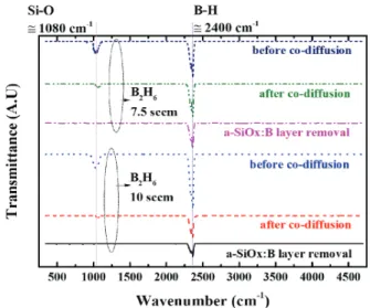
그림 6의 FTIR 분석 결과에서 보듯, a-SiOX:B 박막 은 thermal annealing을 거치면서 Si-O peak이 감 소되는 경향을 보이며 a-SiOX:B 박막 제거되었을 때 Si-O peak이 사라지는 것을 확인하였다. 또한 B-H peak의 경우 a-SiOX:B막이 제거 되면서 다소 감소하 는 경향을 보이지만 hydrogen에 의한 defect로 작용 하는 boron의 부동태화로 인해 MCLT의 증가되는 경 향을 보이고 있다.
4. 결 론
N-type 실리콘 태양전지의 최적화된 boron emitter 형성을 위한 in-situ oxidation를 통한 boron rich layer를 Borosilicate glass로 변환 후 제거와 a- SiOX:B layer을 이용한 p+ layer형성에 관하여 정리하 였다. in-situ oxidation을 pre-deposition 후 950℃
O2 treatment 5분과 drive-in 후 950℃ O2 treatment 5분을 나눠서 실험한 결과 drive-in 후 O2 treatment 에서 FTIR 측정결과 B-O bonding peak의 감소로 인 해 BSG/BRL을 제거된 것을 확인하였으며 a-SiOX:B Silane (SiH4) [sccm]
2 3
MCLT (μs)
RS
(Ω/sq)
MCLT (μs)
RS
(Ω/sq)
B2H6
(sccm)
5 4.79 111.7 70.82 40.6
7.5 31.91 70.85 75.97 37.31
10 65.58 63.62 103.96 36.05
Table 1. MCLT and RS trend by Silane (SiH4) / Diborane (B2H6) gas flow split for co-diffusion process.
Fig. 5. MCLT trend by silane and diborane flow change for co-diffusion process.
Fig. 6. FTIR analysis by diborane (B2H6) gas flow variation during co-diffusion process.
layer를 plasma enhanced chemical vapor deposition (PECVD) 장비를 이용하여 증착하였다.
tube furnace에서 1,040℃에서 90분간 drive-in하였 고 SiH4 및 B2H6가 높은 a-SiOX:B layer일수록 MCLT 이 높은 결과 값을 확인하였다. FTIR 측정 결과 thermal annealing 후 다소 B-H peak이 감소하지만 hydrogen에 의한 boron의 부동태화에 의해 MCLT가 향상되었다.
감사의 글
This work was supported by the Regional Development program (No. R0005632) of the Korea Institute Advancement of Technology (KIAT) grant funded by the Korea government Ministry of Trade, Industry and Energy.
REFERENCES
[1] A. U. Rehman and S. H. Lee, Scientific World J., 13 (2013).
[2] K. Bothe, R. Sinton, and J. Schmidt, Progress in Photovoltaics, 13, 297 (2005). [DOI: https://doi.org/10.1002/
pip.586]
[3] D. L. Meier, V. Chandrasekaran, H. Preston Davis, A. M.
Payne, X. Wang, V. Yelundur, J. E. O’Neill, Y. W Ok, F.
Zimbardi, and A. Rohatgi, IEEE JOURNAL OF PHOTOVOLTAICS, 1, 123 (2011).
[4] J. Sheng, W. Wang, S. Yuan, W. Cai, Y. Sheng, Y. Chen, J. Ding, N. Yuan, Z. Feng, and P. J. Verlinden, Sol. Energ.
Mat. Sol. Cells, 152, 59 (2016). [DOI: https://doi.org/10.1016/
j.solmat.2016.03.032]
[5] K. Ryu, E. Cho, A. Rohatgi, and Y. Ok, PROGRESS IN
PHOTOVOLTAICS, 24, 1109 (2016). [DOI: https://doi.org/
10.1002/pip.2775]
[6] M. A. Kessler, T. Ohrdes, B. Wolpensinger, R. Bock, and N. P. Harder, Proc. 34th IEEE Photovoltaic Specialists Conference (PVSC) (Philadelphia, USA, 2009) p. 001556.
[7] B. Singha and C. S. Solanki, Semicond. Sci. Technol, 31, 10 (2016). [DOI: https://doi.org/10.1088/0268-1242/31/3/035009]
[8] S. P. Phang, W. Liang, B. Wolpensinger, M. A. Kessler, and D. Macdonald, IEEE JOURNAL OF PHOTOVOLTAICS, 3, 261 (2013). [DOI: https://doi.org/10.1109/JPHOTOV.2012.
2226332]
[9] K. Ryu, C. J. Choi, H. M. Park, D. H. Kim, A. Rohatgi, and Y. W. Ok, Sol. Energ. Mat. Sol. Cells, 146, 58 (2016).
[DOI: https://doi.org/10.1016/j.solmat.2015. 11.031]
[10] J. Y. Cho, H.N.R. Shin, J. E. Lee, Y. S. Choi, J. C. Lee, H. Ph, T. J. Kim, M. I. Hwang, and E. C. Cho, Energy Procedia, 77, 279 (2015). [DOI: https://doi.org/10.1016/j.
egypro.2015.07.039]
[11] P. Rothhardt, C. Demberger, A. Wolf, and D. Biro, Energy Procedia, 38, 305 (2013). [DOI: https://doi.org/10.1016/j.
egypro.2013.07.282]
[12] N. Wehmeier, B. Lim, A. Merkle, A. Tempez, S. Legendre, H. Wagner, A. Nowack, T. Dullweber, and P. P. Altermatt, IEEE JOURNAL OF PHOTOVOLTAICS, 6, 119 (2016).
[DOI: https://doi.org/10.1109/JPHOTOV.2015.2493364]
[13] P. Negrini, A. Ravaglia, and S. Solmi, J. Electrochem, 125, 609 (1978). [DOI: https://doi.org/10.1149/1.2131510]
[14] J. Engelhardt, A. Frey, L. Mahlstaedt, S. Gloger, G. Hahn, and B. Terheiden, Energy Procedia, 55, 235 (2014). [DOI:
https://doi.org/10.1016/j.egypro.2014.08.050]
[15] J. Schön, M. C. Schubert, W. Warta, H. Savin, and A.
Haarahiltunen, Phys. Status Solidi A, 207, 2589 (2010).
[DOI: https://doi.org/10.1002/pssa.201026333]