Vol. 24, No. 3 (2014)
152
Effect of an Au Nanodot Nucleation Layer on CO Gas Sensing Properties of Nanostructured SnO
2Thin Films
Nguyen Le Hung
1,2, Hyojin Kim
1†and Dojin Kim
11Department of Materials Science and Engineering, Chungnam National University, Daeduk Science Town, Daejeon 305-764, Korea
2Department of Physics, Thai Nguyen University of Education, Thai Nguyen, Vietnam
(Received January 2, 2014 : Received in revised form March 16, 2014 : Accepted March 17, 2014)
Abstract We report the effect of the fabric of the surface microstructure on the CO gas sensing properties of SnO2 thin films deposited on self-assembled Au nanodots (SnO2/Au) that were formed on SiO2/Si substrates. We characterized structural and morphological properties, comparing them to those of SnO2 thin films deposited directly onto SiO2/Si substrates. We observed a significant enhancement of CO gas sensing properties in the SnO2/Au gas sensors, specifically exhibiting a high maximum response at 200oC and quite a low detection limit of 1 ppm level in dry air. In particular, the response of the SnO2/Au gas sensor was found to reach the maximum value of 32.5 at 200oC, which is roughly 27 times higher than the response (~1.2) of the SnO2 gas sensor obtained at the same operating temperature of 200oC. Furthermore, the SnO2/Au gas sensors displayed very fast response and recovery behaviors. The observed enhancement in the CO gas sensing properties of the SnO2/Au sensors is mainly ascribed to the formation of a nanostructured morphology in the active SnO2 layer having a high specific surface- reaction area by the insertion of a nanodot form of Au nucleation layer.
Key words tin oxide, nanostructured oxide, gas sensor, Au nanodot, sputtering.
1. Introduction
Recent anthropogenic environmental destruction and ecological crisis are urgently demanding relevant gas sensors for detecting various harmful air pollutants in- cluding carbon oxides and nitrogen oxides. In the field of solid-state gas sensors, chemiresistive gas sensors based on semiconducting metal oxides have been extensively investigated since the observation of the gas sensing effect in zinc oxide(ZnO) thin films via a change in electrical resistivity for a variation of the gas composition by Seiyama et al. as early as 1962.1) Among useful semi- conducting metal oxides as sensing materials, tin oxide (SnO2) and tungsten oxide(WO3) are known to be two of the most reliable materials for the fabrication of semi- conducting metal oxide gas sensors. These two oxides are the actual sensing materials used in commercial gas sensing devices: SnO2 for the detection of reducing gases like carbon monoxide(CO) and WO3 for the oxidizing gases like nitric oxide(NO).2) Here we are concerned
with SnO2.
It is well known that for traditional bulk or thin-film SnO2 gas sensors, due to the limited surface-to-volume ratio, only a small fraction of the gas species adsorbed onto the exposed surface is active in modifying the electrical resistivity, leading to a low detection per- formance.3) Thus many efforts have been made to modify the active surface layers of SnO2 or fabricate this oxide material in different forms, overcoming several inherent limitations of SnO2-based gas sensors: high operating temperature, low maximum sensitivity and slow response.
On the one hand, the introduction of dopants and/or catalytic elements into SnO2 has been attempted as an effective way for an enhancement in gas detection per- formance.4-10) On the other hand, one of the most pro- mising approaches recently developed for improving gas sensing properties is the fabrication of SnO2-based nano- structured sensing materials.9-13) For that matter, in the case of ZnO thin film gas sensors was reported a novel simple technique, which is here attempted on SnO2-based
†Corresponding author
E-Mail : [email protected] (H. Kim, Chungnam Nat'l Univ.)
©Materials Research Society of Korea, All rights reserved.
This is an Open-Access article distributed under the terms of the Creative Commons Attribution Non-Commercial License (http://creative- commons.org/licenses/by-nc/3.0) which permits unrestricted non-commercial use, distribution, and reproduction in any medium, provided the original work is properly cited.
thin film gas sensors, for modification of the surface morphology of the active layer by introducing an self- assembled Au nanodot layer as a nucleation layer, leading to an enhancement of gas sensing properties.14)
Here our attention is focused on the detection of the carbon monoxide(CO) gas which is one of the most dangerous gases. Since CO is a colorless, odorless and tasteless compound produced by incomplete combustion of carbon-containing materials, CO detection in an en- vironment is impossible without using any detection device. So CO is often referred to as the “silent killer”
because most beings do not find themselves being poi- soned. It is noted that the occupational exposure limit to CO is 35 ppm-10 h,15) and then it is needed to develop highly sensitive CO gas sensors.
In this study, we investigate the effects of the self- assembled Au nanodot nucleation layer on the surface morphological properties as well as the CO gas sensing properties of SnO2-based thin film gas sensors. Our SnO2- based thin film gas sensors exhibit a highly sensitive, reversible and fast response to CO even at quite low CO concentrations and at relatively low operating tempera- tures, confirming that the simple microstructure modifi- cation technique via introducing an Au nanodot nucleation layer can be easily applied to relevant semiconducting metal oxide thin films for improving the gas sensing properties.
2. Experimental Procedure
The SnO2/Au thin film gas sensing elements were fabricated just following the previously reported pro- cedure.14) To begin with, a pair of parallel Pt/Ti electrodes was deposited on the SiO2/Si (100) substrates by dc sputtering using a shadow mask. Secondly, a thin Au layer with the thickness of 2 nm was deposited on the whole substrate area by dc sputtering. Annealing the Au layer at 500oC in a nitrogen atmosphere for 30 min resulted in the formation of the self-assembled Au layer consisting of isolated Au nanodots. Finally, a SnO2 thin film with the thickness of about 100 nm was deposited by rf sputtering as the active layer in a chemiresistive sensor element. As a consequence, a gas sensing element comprises the SnO2-based active layer with the embedd- ed Pt/Ti parallel electrodes covered by a self-assembled Au layer consisting of isolated Au nanodots. For com- parison, the SnO2 thin film gas sensing elements without any Au layer were also fabricated in a similar way.
SnO2 thin films were deposited from a Sn metal target by rf sputtering in a mixed gas of Ar and O2 at a ratio of two to one under the working pressure of 5 mTorr at 200oC. Here the substrate temperature of 200oC during deposition was found to be low enough to suppress a
possible coarsening of Au nanodots. The target-to-sub- strate distance was fixed at 12 cm, while the rf power density was maintained at 2.5 W/cm2 for the Sn target.
The thickness of deposited SnO2 films was set to be about 100 nm(estimated from cross-sectional SEM micro- graphs) by adjusting the deposition time.
The crystalline structure of the films was characterized by X-ray diffraction(XRD) using Cu Kα radiation, re- vealing the formation of the polycrystalline tetragonal rutile-type phase of SnO2. Scanning electron microscopy (SEM) was used to observe the morphologies and micro- structures of the SnO2 thin films.
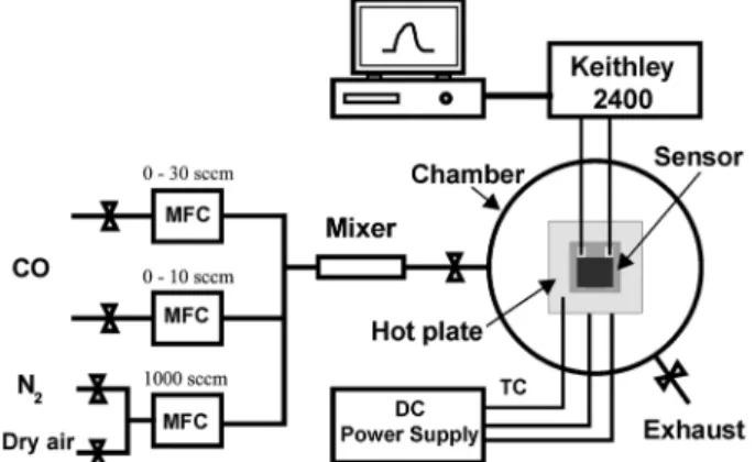
The electrical and CO gas sensing properties of the fabricated gas sensing elements were measured via two conductive electrodes by a multi-meter(Keithley 2400) assembled in a computer-controlled gas sensing charac- terization system, which is schematically shown in Fig.
1, using flow-through method as mentioned in detail in Ref. [14]. To reduce the delay in response caused by the inner dead volume of the measurement chamber(~500 mL), we used an adapter tube to expand the inlet port near the active surface of the gas sensing elements so that gas flow can reach the active area much faster than the diffusion flow coming from the original inlet port.
The operating temperature was controlled and maintained constant in the range from 150 to 350oC during data acquisition periods using a small isolated hot plate integrated in the measurement chamber connected to a temperature controller. Prior to the start of each measure- ment, the sensors were pre-heated at 400oC for several hours in order to remove the surface-adsorbed layer of contaminants from the SnO2 sensing layers and then cooled to the measurement temperature. The sensor re- sponse Sg is defined as Sg=∆G/Ga= (Gg− Ga)/Ga= (Ra− Rg)/Rg for a reducing gas such as CO gas, where Ga and Gg (or Ra and Rg) are the electrical conductance (or electrical resistance) in dry air and upon exposure to the target gas in dry air, respectively.14,16)
Fig. 1. Schematic diagram of a computer-controlled gas sensing characterization system.
3. Results and Discussion
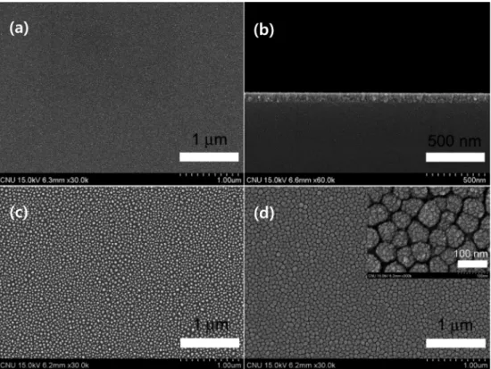
In Fig. 2, we show typical microstructures of a SnO2 thin film deposited directly onto a SiO2/Si (100) substrate without any Au layer [shortly designated as SnO2] and a SnO2 thin film deposited onto the self-assembled Au nanodots [shortly designated as SnO2/Au] with the nearly same thickness of about 100 nm. We first present the top- view and cross-sectional SEM micrographs of the SnO2
thin film, respectively in Figs. 2(a) and 2(b), showing quite a compact flat surface with a dense non-columnar structure. In contrast, as presented in Fig. 2(d), the top-
view SEM micrograph of the SnO2/Au thin film indicates a distinct uniform microstructure with an average grain size of about 50 nm. It is here noted that we confirm the formation of the self-assembled Au nanodots as revealed evidently in Fig. 2(c). From Figs. 2(a) and 2(d), the surface roughness of the SnO2/Au thin film is seen to be much higher than that of the SnO2 thin film. A whole surface of the SnO2/Au thin film opens up with the formation of abundant nanotrenches surrounding each grain with the width of around 50 nm. Moreover, as observed on the inset of Fig. 2(d), each grain seems to contain many fine nanograins whose size ranges from several to ten nm,
Fig. 3. (a) I-V characteristic curves of the SnO2/Au thin film gas sensor at various operating temperatures in dry air. (b) Variation of the resistance as a function of the operating temperature for the SnO2/Au thin film gas sensor in dry air.
Fig. 2. (a), (b) Typical top-view and cross-sectional SEM images of SnO2 thin films deposited directly onto a SiO2/Si (100) substrate.
(c) SEM image of self-assembled Au nanodots. (d) Typical SEM image of SnO2 thin films deposited onto the self-assembled Au nanodots.
The inset shows the high-magnification SEM image of the SnO2/Au thin film.
which is equivalent to that of the Au nanodots. As a consequence, such a microstructure is expected to give greater surface area and provide active adsorption sites.
These results demonstrate a crucial effect of the self- assembled Au nanodots as nucleation sites on the micro- structure of the SnO2 thin films.
Fig. 3(a) shows the typical current-voltage(I-V) charac- teristics of SnO2/Au thin film gas sensors with the thick- ness of about 100 nm at various operating temperatures in dry air. The three(I-V) curves show a good ohmic contact behavior between the SnO2/Au thin film and the Pt/Ti electrodes with a linear relationship between the applied voltage and the resulting electric current at different working temperatures, satisfying the requirement for a chemiresistive gas sensor.
Fig. 3(b) shows the resistance-temperature curves of a SnO2/Au thin film gas sensor in dry air. It can be seen that the SnO2/Au thin film sensor exhibits both the negative(NTCR) and positive temperature coefficient of resistivity(PTCR) characteristics, revealing a semiconduc- ting-like behavior from 50 to 100oC followed by the PTCR characteristics from 100 to 200oC and a semicon- ducting-like behavior again above 200oC. This observed behavior is normally explained by a typical surface-con- trolled model.17) In this case of a semiconducting metal oxide, the PTCR characteristic observed in the temperature range from 100 to 200oC can be mainly ascribed to the role of oxygen. Indeed, when a SnO2-based gas sensor is exposed to air, oxygen from the ambient adsorbs on the exposed SnO2 surface to form mainly O2−, O− or O2−
depending on the operating temperature by capturing electrons from the SnO2 conduction band, according to the following surface reactions: O2(gas)→ O2(ads); O2 (ads) + e−→ O2−(ads); O2−(ads) + e−→ 2O−(ads); O−(ads) + e−→ O2−(ads). This creates a depletion layer near the surface together with surface acceptor states related to oxygen adsorption and lowers the conductivity, thus re- sulting in an increased electrical resistivity when the sensor works in the presence of oxygen in the ambient.
The observed PTCR characteristic thus originates from the increase in the surface acceptor state density due to the charge transfer process between oxygen from the coming air flow and SnO2 surface and/or the change in charge state of the pre-chemisorbed oxygen species with increasing temperature. Above 200oC the resistance again decreases, which indicates the recovery of the typical semiconducting electrical behavior governed by the thermally-activated generation of electrical carriers.
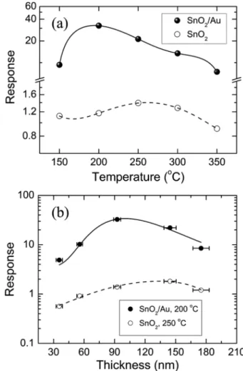
Fig. 4 shows the typical behaviors in the response Sg of the SnO2 gas sensors with and without a self-assembled Au nucleation layer, for sensing 20 ppm CO in dry air.
In Fig. 4(a), we present the observed variations of the CO gas sensing response as a function of operating
temperature for the SnO2/Au and SnO2 thin film gas sensors with the nearly same thickness of SnO2 layer of about 100 nm. It is obviously seen here that the introduc- tion of the Au nucleation layer results in a remarkable increase in the CO gas sensing response for the SnO2- based thin film gas sensors. The response of the SnO2/Au gas sensor is found to reach the maximum value of 32.5 at 200oC, which is roughly 27 times higher than the response(about 1.2) of the SnO2 gas sensor obtained at the same operating temperature of 200oC. Furthermore, this maximum response is higher than the response re- ported for some other forms of SnO2-based CO gas sensors operated at 200oC and higher temperatures.4,10,13,18)
These results suggest that the SnO2/Au thin film gas sensor has a very high sensitivity to CO gas at relatively low temperatures. The observed enhancement in the CO gas sensing response of the SnO2/Au thin film gas sensors is primary due to a strong variation in the mor- phology of the SnO2 active layer, as shown in Fig. 2. In the case of the SnO2 thin film, as clearly seen in Figs.
Fig. 4. Variations of the CO gas sensing response (a) as a function of the operating temperature and (b) as a function of the SnO2 film thickness for the SnO2/Au gas sensor (solid circles) and SnO2 gas sensor (open circles) when exposing to 20 ppm CO in dry air.
2(a) and 2(b), its dense morphology seems to impose some constraints on the surface-to-volume ratio as well as available sites for oxygen adsorption. The relatively small exposed active surface area is thus supposed to be responsible for the low response in the SnO2 thin film sensor. In contrast, the SnO2/Au film could provide much more active surface area, originated from its much rougher surface morphology together with abundant nanotrenches surrounding each SnO2 grain(see Fig. 2(d)), consequently leading to the enhancement of the CO gas sensing response.
Fig. 4(b) shows the variations of the CO gas sensing response as a function of SnO2 ceramic film thickness for the SnO2/Au and SnO2 thin film gas sensors. The SnO2/ Au gas sensor exhibits a very high maximum response to CO gas in dry air at the optimal operating temperature of 200oC at a thickness of SnO2 ceramic film of about 100 nm, whereas the SnO2 gas sensor shows even lower maxi- mum response at its own optimal operating temperature of 250oC at a thickness of SnO2 ceramic film of about 150 nm. As a consequence, the optimal thickness of SnO2 layer and the optimal operating temperature for the SnO2/Au thin film gas sensors are about 100 nm and 200oC, respectively. It thus reveals a trend in increasing response together with decreasing optimal operating tem- perature for the SnO2/Au thin film gas sensor in com- parison with the SnO2 thin film gas sensor. It is worth- while to note here that even though the thickness of our SnO2/Au thin films is as thick as 100 nm, we cannot entirely ignore the possibility that Au diffuses into the active surface during fabrication and acts as a catalyst, which could be another possible factor for the enhance- ment in the CO gas sensing response.
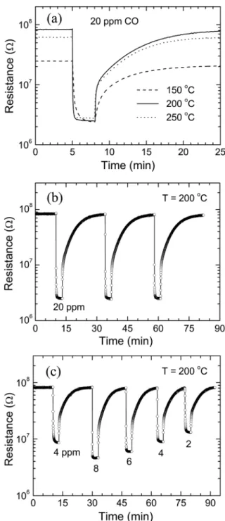
Fig. 5 shows the dynamic resistance response curves of the SnO2/Au thin film gas sensor to CO gas in dry air under various measurement conditions. Usually, the re- sponse characteristics of a gas sensor depend on the operating temperature. In Fig. 5(a), we present the resis- tance response curves of the SnO2/Au thin film gas sensor for a CO gas concentration of 20 ppm in dry air at various operating temperatures of 150, 200 and 250oC.
At each temperature, the initial resistance of the sensor in the dry air is high and steady, whereas its resistance de- creases abruptly when it is exposed to CO gas, exhibiting n-type semiconducting behavior as expected. As clearly seen in Fig. 5(a), the response curve at 200oC exhibits both higher magnitude and faster speed of response to CO gas compared to those at other operating temperatures.
In general, the gas sensing mechanism of the semicon- ducting metal oxide gas sensors is based on a variation in the electrical resistance or conductance due to gas adsorp- tion and desorption on the active surface. When dry air is used as carrier gas, the formation of the adsorbed oxygen
species make the sensor have quite a high initial resistance as previously discussed. When the sensor is exposed to CO, the CO gas reacts with the adsorbed oxygen species, producing CO2 molecules and releasing electrons back into the conduction band: 2CO + O2−→ 2CO2+ e− ; CO + O−→ CO2+ e− ; CO + O2−→ CO2+ 2e−. These reactions cause an increase in conductivity and, as Fig. 5. Typical resistance response curves of the SnO2/Au thin film gas sensors: (a) for a CO gas concentration of 20 ppm in dry air at various operating temperatures, (b) during periodical exposure to 20 ppm CO in dry air at an operating temperature of 200oC, and (c) for various CO gas concentrations in dry air at 200oC.
observed, the resistance of the SnO2/Au gas sensor is decreased.
In Fig. 5(b), we present the typical resistance response curve of the SnO2/Au thin film gas sensor during peri- odical exposure to 20 ppm CO in dry air at its optimal operating temperature of 200oC, showing almost the same three cycles of response-recovery behavior with very quick response. These reversible cycles of the response curve indicate a stable and repeatable behavior of the SnO2/Au thin film gas sensor in detecting CO gas at 200oC. The response time, defined as the time taken for the sensor to attain 90 % of the saturation resistance upon exposure to the target gas, was estimated to be about 2 s at 20 ppm CO in dry air at the operating temperature of 200oC, being quite the same as that of SnO2 hollow nanofibers(0.7 s for 100 ppm CO) operated at 385oC,10) but much shorter than those of some other forms of SnO2-based CO gas sensor, including SnO2-Pd thin films (~2 min for 150 ppm CO) operated at 200oC as well as SnO2 nanoparticles and nanorods(100 s for 1000 ppm CO) at 200oC.4,13) Furthermore, the SnO2/Au thin film gas sensor exhibits a good response-recovery performance to CO gas at different CO concentrations in dry air, particularly even at quite low concentrations, having low detection limit of ppm level, as seen in Fig. 5(c). Also, there seems to be no fluctuation and shift in the baseline resistance during many consecutive measurement cycles, indicating good thermal stability of the SnO2/Au thin film gas sensor.
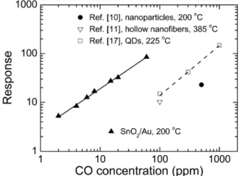
Fig. 6 shows our sensor’s response as a function of CO gas concentration in dry air at 200oC along with those of different forms of SnO2-based gas sensors previously reported. It is obviously seen that the SnO2/Au thin film
gas sensor developed in this study has a higher CO gas sensitivity compared with the sensors based on SnO2
nanoparticles,13) SnO2 hollow nanofibers,10) or SnO2 quan- tum dots(QDs).18) The solid straight line drawn through the experimental data represents the fitted curve for the measured data set using the following empirical equation Sg=Ag(Pg)β, where Pg is the target gas partial pressure, which is proportional to the gas concentration, Ag is a prefactor and β is the exponent on Pg.16) From the fitted data, β is found to be 0.83 ± 0.01. It is well known that the value of β is dependent on the state of the adsorbed oxygen species and the microstructure of the active layer.
This estimated result indicates that the primary adsorbed oxygen species on the SnO2/Au thin film surface at 200oC are mixture of O− and O2−.
4. Conclusions
In conclusion, we have developed an effective and readily available technique for surface morphology modi- fication, which could be highly adaptable to any semi- conducting metal oxide thin films via introducing self- assembled Au nanodots as a nucleation layer. It has been demonstrated in this study that nanostructured SnO2 thin films deposited on self-assembled Au nanodots shows a large enhancement of CO gas sensing properties, in turn resulting in excellent CO sensing performance. In par- ticular, the SnO2/Au thin film gas sensor shows a highly sensitive, reversible and fast response to CO gas in dry air at relatively low optimum operating temperature and even at low range of CO concentration. Actually, the ob- served enhancement can be attributed to the intensifi- cation of the surface reaction between chemisorbed oxygen ions and CO reducing gas, which is considered to result primarily from the definite formation of SnO2 nanostruc- ture having a wide and uniform network of nanotrenches by introducing a Au nucleation layer. These results illustrate that the SnO2 thin films deposited on self- assembled Au nanodots are promising for large scale fabrication of cost-effective and high-performance CO gas sensors operable at low CO concentrations and tem- peratures.
Acknowledgements
This work was supported by the National Research Laboratory Program and the grant funded by the National Research Foundation of Korea(NRF-2013R1A1A4A010- 07571).
References
1. T. Seiyama, A. Kato, K. Fujiishi and M. Nagatani, Anal.
Fig. 6. Variation of the CO gas sensing response as a function of CO gas concentration for the SnO2/Au thin film gas sensor operated at 200oC, in comparison with those of some different forms of SnO2-based gas sensors. The solid line is the fit curve of the empirical model.
Chem., 34, 1502 (1962).
2. M. Hübner, C. E. Simion, A. Haensch, N. Barsan and U.
Weimar, Sens. Actuators B, 151, 103 (2010).
3. S. W. Lee, P. P. Tsai and H. Chen, Sens. Actuators B, 67, 122 (2000).
4. R. Rella, A. Serra, P. Siciliano, L. Vasanelli, G. De and A.
Licciulli, Thin Solid Films, 304, 339 (1997).
5. J. H. Sung, Y. S. Lee, J. W. Lim, Y. H. Hong and D. D.
Lee, Sens. Actuators B, 66, 149 (2000).
6. A. Khanna, R. Kumar, and S. S. Bhatti, Appl. Phys. Lett., 82, 4388 (2003).
7. I. Fasaki, M. Suchea, G. Mousdis, G. Kiriakidis and M.
Kompitsas, Thin Solid Films, 518, 1109 (2009).
8. G. Korotcenkov, B. K. Cho, L. Gulina and V. Tolstoy, Sens. Actuators B, 141, 610 (2009).
9. H. Huang, C. Y. Ong, J. Guo, T. White, M. S. Tse and O. K. Tan, Nanoscale, 2, 1203 (2010).
10. J. K. Choi, I. S. Hwang, S. J. Kim, J. S. Park, S. S. Park, U. Jeong, Y. C. Kang and J. H. Lee, Sens. Actuators B, 150, 191 (2010).
11. G. Neri, A. Bonavita, G. Rizzo, S. Galvagno, N. Pinna, M.
Niederberger, S. Capone and P. Siciliano, Sens. Actuators B, 122, 564 (2007).
12. Y. Wang, X. Jiang, and Y. Xia, J. Am. Chem. Soc., 125, 16176 (2003).
13. B. M. Matin, Y. Mortazavi, A. A. Khodadadi, A. Abbasi and A. A. Firooz, Sens. Actuators, B 151, 140 (2010).
14. N. L. Hung, H. Kim, S.-K. Hong and D. Kim, Sens.
Actuators B, 151, 127 (2010).
15. NIOSH Pocket Guide to Chemical Hazards, 3rd ed., National Institute for Occupational Safety and Health, Cincinnati (2007).
16. R. J. S. Scott, S. M. Yang, G. Chabanis, N. Coombs, D.
E. Williams and G. A. Ozin, Adv. Mater., 13, 1468 (2001).
17. M. Takata, D. Tsubone and H. Yanagida, J. Am. Ceram.
Soc., 59, 4 (1976).
18. S. M. Sedghi, Y. Mortazavi and A. Khodadadi, Sens.
Actuators B, 145, 7 (2010).