대 전류 응용 위한 유도 부하를 갖는 위상 변이 풀 브릿지 컨버터의 전류 제어기 설계
(Current Controller Design of a Phase Shift Full Bridge Converter for High Current Applications with Inductive Load)
레 덧 탕1), 박 민 원2), 유 인 근3)*
(Tat-Thang Le, Min-Won Park, and In-Kun Yu)
요 약 본 논문에서는 유도성 부하를 가지는 위상 변위 풀 브릿지 컨버터(PSFB)의 성능과 다
양한 유도성 부하를 갖는 출력 전류의 동적 응답을 향상시키는 새로운 전류 제어 기법을 제안하였 다. 누설 인덕턴스 및 유도성 부하를 포함하는 향상된 동적 모델을 사용하였으며, 유도 부하의 변화 에 대한 영향을 상세히 분석하였다. 제안된 전류 제어 방식은 위상 여유 사양을 기반으로 설계하였 다. 결과적으로 제안된 전류 제어 기법은 기존의 전류 제어 기법과 비교하여 동적 응답을 개선시킬 수 있음을 확인하였다. 설계된 컨트롤러의 성능은 500 A PSFB 컨버터 시스템을 통하여 검증하였 다. 이 결과는 초전도 장치와 같이 유도성 부하가 큰 고 전류 애플리케이션에 활용할 수 있다.
핵심주제어 : 고 전류, 위상변위 풀 브릿지 (PSFB), 전류 제어기
Abstract This paper presents the performance of a Phase Shift Full Bridge (PSFB) converter with inductive load and a new current control scheme to improve dynamic response of output current with various inductive loads. Enhanced dynamic model is used which includes leakage inductance and inductive load. Effect of changing of inductive load was analyzed in detail. Proposed current control scheme is designed based on phase margin specifications. As a result, the proposed current control scheme helps to improve the dynamic response in comparison with the existing current control scheme. The performance of the designed controller is verified by a 500 A PSFB converter. The results will be utilized for high current applications with high inductive load such as superconducting devices.
Key Words : High current low voltage, Phase shift full bridge (PSFB), Current controller
* Corresponding Author : [email protected]
+ 이 논문은 2016년 - 2017 년 창원대학교 연구비에 의하여 연구되었음.
Manuscript received August 18, 2017 / revised January 29, 2018 / accepted February 20, 2018
1) 창원대학교 전기공학과, 제1저자
2) 창원대학교 전기공학과, 제2저자
3) 창원대학교 전기공학과, 제3저자
1. Introduction
In high current applications with high inductive load such as superconducting cable, high temperature superconducting (HTS) DC induction heating machine and HTS DC reactor [1]-[3], Phase Shift Full Bridge (PSFB) converter is widely used with benefits of Zero Voltage Switching (ZVS). The high current applications require high performances of the power converter, particularly in terms of high current capacity, DC stability and dynamic response. The topology of the converter was proposed in [4], [5]. The dynamic response depends not only on the parameters of converter but also load types [6]. In general, high inductive load makes output current low response. Normal current controller design method is difficult to control output current with the various value of inductive load.
In this paper, a precise model is presented and a new current control scheme is proposed to improve the dynamic response of the converter with various inductive load.
Enhanced dynamic model is used which allows the joint investigation of the influence of the transformer characteristics (turns ratio and leakage inductance) and inductive load.
Following this way, the dynamic behavior of the converter is performed in detail. The impact of high inductive load is analyzed. The resonant peak caused by large inductive load is attenuated by employing the advantage of the notch filter. This filter is considered as a combination of low pass and high pass filters.
The characteristic of the filter depends on notching frequency and the damping ratio.
Proposed current control scheme was designed based on phase margin specifications and the
wide range of output inductive load, in which the control coefficient is added for various value of inductive load. Stability and dynamic response of the converter which includes overshoot, steady-state error are analyzed by considering the parameters of bode diagram.
The phase margin and crossover frequency of the controller are selected so that overshoot and steady-state error can be minimized.
The proposed current control scheme helps to improve the dynamic response in comparison with existing current control schemes. In the normal current controller, the response time and overshoot are increased with respect to increasing of inductive load.
The proposed current controller overcame these issues by means of the control coefficient. The steady-state error is reduced by increasing magnitude at the range of low frequency. On the other hand, output current response can be improved by compensating the phase margin and crossover frequency. The performance of the designed controller was verified by a 500 A PSFB converter application.
2. Modeling and Analysis
2.1 Precise modelling
Figure 1 shows the circuit diagram of the
PSFB converter for high current low voltage
applications. The system consists of a bridge
rectifier and a PSFB converter with series
connected transformers. This type of
connection will make the output current of
each transformer balanced and easy to control
compared with parallel connected transformers.
In order to achieve soft switching in a PSFB converter, the energy in the total leakage inductance of transformers needs to be enough to charge and discharge capacitors. If it is not enough, the external inductor has to be added to the primary side in series with transformers. However, the circulating current is increased by the too high value of primary inductance.
Fig. 1 Circuit diagram of PSFB converter.
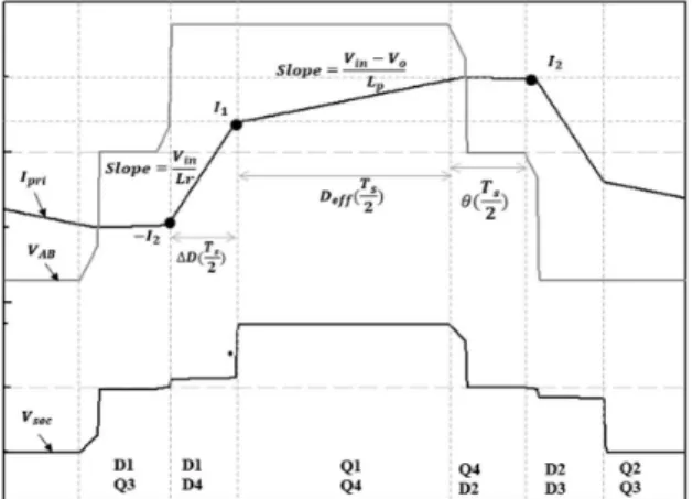
Fig. 2 Circuit waveforms of PSFB converter.
On the other hand, the slope of the current reduces the duty-cycle of secondary side voltage as shown in Fig. 2. Effective duty (
) represents the power delivery mode.
From [4] and Fig. 2,
is given as:
∆
′(1)
where is the duty cycle of the primary voltage, ∆ is the duty cycle loss due to the finite slope of the rising and falling edges as shown in Fig. 2,
is the transformer turns ratio, m is the number of transformer connected in series,
and
are the converter input and output voltages, respectively,
is the switching frequency,
is the output filter inductor and
, Effective duty depends on the output inductor current
,
,
, therefore, the small signal also depends on these parameters. The small signal model of effective duty is given from [7]:
(2)
where
is the change of output filter inductor current,
is the change of input voltage, is the small signal of primary voltage duty cycle. The derived PSFB model in [8] does not include the inductive load which contributes to the dynamic response of the converter. The PSFB small signal model in Fig. 3 is considered, where
[8]
The contribution of
and
are represented by two controlled sources and the contribution of is represented by two independent sources. Referring to Fig. 3, the transfer function of duty-to-output is obtained in equation (3). The transfer function
represents the sensitivity of the output current
to duty cycle variations. In high current power
supply, the current controller has to be
designed. The transfer function
is the
most important in the control loop design.
(3)
where
In this model, the output inductance
was considered, the impact of output inductance is analyzed in the following subsection.
Fig. 3 Small-signal model of PSFB with series transformer
2.2 Dynamic response analysis
The parameters of PSFB converter for high current applications were optimally designed based on the reduction of switching and conduction loss techniques [9], [10]. Specifications of the system are listed in Table 1.
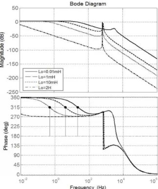
Figure 4 shows the bode diagram of the plant as the inductive load changes from 1 to 2 . As a result, the crossover frequency decreases with respect to increase of the inductive load, results in decrease of output current response. On the other hand, in the case of high inductive load, it appears the resonant peaks at frequency of 0.67 kHz, 0.68
Parameters Symbol Value
Input voltage
513 VOutput current
500 ATransformer ratio
1:12Primary inductance
40
Output inductance filter
220
Output capacitor filter
125
Internal resistance ofcapacitor
0.15
Number of transformer
2 Switching frequency
25 kHz Output inductive load
0: 2HTable 1 Specifications of PSFB
kHz and 1.22 kHz, this makes the system unstable when the controller increases the gain at low frequency for reducing the steady-state error.
Fig. 4 Bode diagram of the plan in the case of
various inductive load
3. Design of a Current Control Scheme
Based on the analysis results in Section 2, the current controller is designed to make sure that steady-state error is reduced by increasing the gain margin at the range of low frequency. The resonant peak caused by large inductive load needs to be damped. On the other hand, output current response can be improved by compensating the phase margin and crossover frequency. In order to do so, the compensator type II combined with notch filter is designed. The new control scheme is proposed for various inductive load.
3.1 Notch Filter
A notch filter is considered as a combination of low pass and high pass filters. A second-order notch filter has the transfer function as:
(4)
where
is the notching frequency, the damping ratio
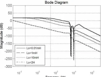
determines the rejection bandwidth of notch filters. In order to avoid the resonant peaks of the plant, the notching frequencies are selected as in Fig. 5 which are 0.67 kHz, 0.68 kHz and 1.22 kHz with small damping ratio. The result in Fig. 6 shows the benefit of notch filters with respect to various inductive load from 0.01 mH to 2 H.
Fig. 5 Transfer functions of notch filter
Fig. 6 Magnitude responses of the notch filters with the different
3.2 Stability analysis
The plant includes notch filters, in order to achieve minimal overshoots, zero steady-state error, some parameters of bode diagram was considered:
∙ The steady-state error is zero if the compensator has a pole at the origin which makes the high gain margin at the range of low frequency.
∙ Crossover frequency directly influences to
the pole-zero location of the compensator; it
has to be judiciously selected to get optimum
performance. Fig. 6 shows the possible range
for crossover frequency selection which is smaller than the notching frequency
∙ Overshoot is affected by phase margin.
The closed loop performances are shown in Fig. 7 with different values of compensator phase margin for a fix crossover frequency of 0.157 kHz and
. It is clear that for
is small, the performance exhibits more overshoots before reaching steady-state point.
Fig. 7 Step response for different phase margin of compensator
3.3 Proposed control scheme
From pervious section, the crossover frequency has been reduced when the inductive load increases, it is easy to see that the compensator can compensate the frequency response by only increase the coefficient so that the system can achieve at the same frequency and phase margin in the case of various inductive load. Figure 8 and Table 2 show the values of control gain
with respect to output
inductive load under the condition of compensating crossover frequency at 0.165 kHz and phase margin at
for various value of inductive load.
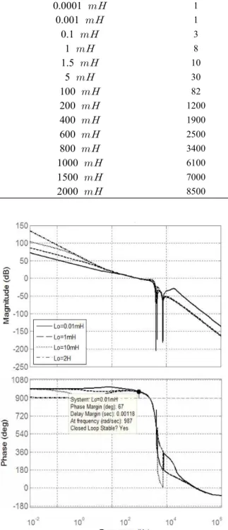
Inductive load
Control gain
0.0001
10.001
10.1
31
81.5
105
30100
82200
1200400
1900600
2500800
34001000
61001500
70002000
8500Table 2 Control gain with respect to inductive load
Fig. 8 Closed-loop transfer function with proposed control scheme
Based on the optimal consideration of phase
margin and crossover frequency, the new
control scheme was proposed and demonstrated in Fig. 9. After measuring output current, the error between set point and measured signal was filtered by using notch filters
. The type II controller
includes a pair of pole-zero combination with a pole at origin as shown in equation 5, the parameters of this controller are designed based on bode diagram analysis [12]
(5)
where
and
are the zero and pole frequencies, respectively. The controller
is multiplied by control gain
, which is estimated from the output inductance
. Value of
is estimated by lookup table technique from Table 2 .
is the PWM modulator gain which converts the control signal to duty cycle and is given as
where
is the peak of the PWM voltage ramp signal.
Fig. 9 Simplified block diagram of the proposed control scheme
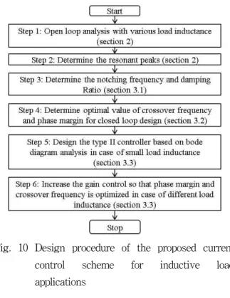
The design procedure of the proposed current control scheme for load induction applications is shown in Fig. 10.
Fig. 10 Design procedure of the proposed current control scheme for inductive load applications
4. Results and Discussions
In order to evaluate the performance of the proposed control scheme, a simulation was conducted in comparison with the conventional current controller. The specifications of the investigated system are listed in Table 1.
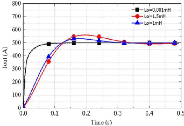
Figure 11 shows the responses of output current with various inductive load in the case of using only one controller. The output current set point is 500 A. The results illustrated low output response and high overshoot with respect to increasing value of
. These drawbacks were avoided by using
the proposed control scheme as resulted in
Fig. 12. When
increases from 0.001 mH to
1.5 mH, the system estimates the coefficient of
the controller
to ensure the optimal value
of phase margin and crossover frequency as
analyzed in Section 3.
Fig. 11 Output current response with a conventional controller
Fig. 12 Output current response with the proposed control scheme
5. Conclusion
In this paper, the authors presented a novel current control scheme for PSFB used in high current applications with various values of inductive load. The precise model of PSFB was considered. The bode diagram has shown that the dynamic response of system depends on the specifications of PSFB and inductive load. The proposed control scheme utilized the benefits of the notch filter and compensator type II to compensate the crossover frequency and phase margin. The results show that the
proposed current control scheme helps to improve the dynamic response in comparison with the existing current control scheme. The proposed method can be applied to almost high current applications with inductive loads.
Acknowledgement
This research was financially supported by the Ministry of Education and National Research Foundation of Korea (NRF) through the Human Resource Training Project for Regional Innovation.(2014H1C1A1066941)
References
[1] Kim, K., Kim, S.K., Park, M., Ha, H.S., Sohn, M.H., Sim, K., Lee, H., and Yu, I.K., “Design and Operating Characteristic Analysis of D-Shape HTS Coil for 1500-A 400-mH Class Toroid-Type HTS DC Reactor,” IEEE Transcactions on Applied Superconductivity, Vol.
26, No. 3, 2016.
[2] Choi, J.H., Kim, K.M., Kim, S.K., Kim, S.H., and Simb, K.D., Park, M.W., and Yu, I.K., “Design and Performance Analysis of an Iron Core-based No-Insulation HTS Magnet for HTS DC Induction Heating Machine,” 28th International Symposium on Superconductivity (ISS 2015), pp.
149-153, 2016.
[3] Kim, S.K., Dinh, M.C., Choi, J.H., Park, M.W., Yu, I.K., Lee, S.J., and Sim, K.D.,
“Transposition-Based Connection Scheme and JointBox Concept for a Tri-Axial HTS Power Cable,” IEEE Transaction on Applied Superconductivity, Vol. 25, No. 3, 2015.
[4] Colak, I., Tuncay, N., “High Current, Low
Voltage Modular Power Converter for Lead Acid Battery Charging,” IEEE ICSET, pp. 1042-1046, 2008.
[5] Kim, Y.D., Cho, K.M., Kim, D.Y., and Moon, G.W., “Wide-Range ZVS Phase-Shift Full-Bridge Converter with Reduced Conduction Loss Caused by Circulating Current,” IEEE Transactions on Power Electronics, Vol. 28, No.
7, pp. 3308-3316, 2013.
[6] Bordry, A.F., Montabonnet, V., Thiesen, H., Kniegl, G., Pauls, R., Wolfes, B., “Soft Swithching (ZVZCS) High Current, Low Voltage Modular Power Converter [13kA, 16V],” EPE 2001, pp.1-9, 2001.
[7] Vlatkovic, V., Sabate, J.A., Ridley, Fred, R.B., Lee, C., Cho, B.H., “Small-Signal Analysis of the Phase-Shifted PWM Converter,” IEEE Transactions on Power Electronics, Vol. 7, No.
1, pp.128-135, 1992.
[8] Capua, G.D., Shirsavar, S.A., Hallworth, M.A., and Femia, N., “An Enhanced Model for Small-Signal Analysis of the Phase-Shifted Full-Bridge Converter,” IEEE Transactions on Power Electronics, Vol. 30, No. 3, pp. 1567-1576, 2015.
[9] Le, T.T., Dinh, M.C., Hwang, C.S., Park M.W., and Yu, I.K., “Parameters Design of a Phase Shift Full Bridge Converter with a Resonant Tank for High Direct Current Applications”
International Journal of Electrical and Electronics Engineering Research (IJEEER), Vol. 7, No. 1, pp. 23-32, 2017.
[10] Le, T.T., Le, D.V., Tuvdensuren, O., Dinh, M.C., Hwang, C.S., Park M.W., and Yu, I.K.,
“Novel Design of a Phase Shift Full Bridge Converter with Resonant Tank Circuit for a High Current Power Supply,” The Korean Institute of Electrical Engineers Conference (KIEE), pp. 944-946, 2016.
[11] Sabate, J.A., Vlatkovic, V., Ridley, R.B., Lee, F., Cho, B.H., “Design Considerations for High-Voltage High-Power Full-Bridge Zero-Voltage-Switched PWM Converter,” Proc.
of the 5th Annual Applied Power Electronics Conference and Exposition (APEC’90), pp.
275-284, 1990.
[12] Ghosh, A., Banerjee, S., Sarkar, M.K., and Dutta, P., “Design and Implementation of Type-II and Type-III Controller for DC – DC Switched-Mode Boost Converter by Using K -Factor Approach and Optimization Techniques,”
IET Power Electronics, Vol. 9, No. 5, pp.
938-950, 2016.
레 덧 탕 (Tat-Thang Le)
∙학생회원
∙Hanoi University of Science and Technology 전기공학과 학사
∙창원대학교 전기공학과 석사
∙현재 : 창원대학교 전기공학과 박사과정
∙관심분야 : 전력전자, 신재생 에너지, 초전도 응용
박 민 원 (Min-Won Park)
∙정회원
∙창원대학교 전기공학과 학사
∙일본오사카대학교 전기공학과 석사
∙일본오사카대학교 전기공학과 박사
∙현재 : 창원대학교 전기공학과 교수
∙관심분야 : 신재생 전력변화 시스템, 전력전자 시스 템, RTDS/RSCAD
유 인 근 (In-Keun Yu)