CMOS 아날로그 전류모드 곱셈기의 선형성과 동적범위 향상을 위한 회로설계 기법에 관한 연구
Daniel Juhun Lee
*ㆍ김형민
**ㆍ박소연
***ㆍ노태민
***ㆍ김성권
****A Study on Circuit Design Method for Linearity and Range Improvement of CMOS Analog Current-Mode Multiplier
Daniel Juhun Lee*ㆍHyung-Min Kim**ㆍSo-Youn Park***ㆍTae-Min Nho***ㆍSeong-Kweon Kim****
요 약
이 논문에서는 아날로그 전류모드 인공지능 프로세서에서 핵심 디바이스 중에 하나인 아날로그 전류 모드 곱셈기 회로의 선형성과 동적범위 향상을 위한 설계 기법을 소개한다. 제안하는 회로는 4 quadrant Translinear loop를 NMOS 트랜지스터만으로 구성하여, 트랜지스터의 물리적 Mismatch를 최소화하는 설계로 0.35
CMOS 공정에서 117
x 109
로 구현가능하였으며, 최대 전고조파왜율 0.3% 의 선형성을 확보 할 수 있었다. 제안한 아날로그 전류모드 곱셈기는 전류모드 인공지능 프로세서의 핵심 회로로 유용할 것으로 기대된다.ABSTRACT
In this paper, we present a design method for improving the linearity and dynamic range of the analog current mode multiplier circuit, which is one of the key devices in an analog current mode AI processor. The proposed circuit consists of 4 quadrant translinear loops made up of NMOS transistors only, which minimizes physical mismatches of the transistors. The proposed circuit can be implemented at 117
x 109
in 0.35
CMOS process and has a total harmonic distortion of 0.3%. The proposed analog current mode multiplier is expected to be useful as the core circuit of a current mode AI processor.키워드
CMOS Analog Multiplier, Four Quadrant, Squarer Circuit, Current-Mode, Translinear Loop CMOS 아날로그 멀티플라이어, 4 쿼드런트, 제곱 회로, 전류모드, 트랜스리니어 루프
* 서울과학기술대학교 IT융합공학과 ([email protected])
** 서울과학기술대학교 정보통신미디어공학전공 ([email protected])
*** 서울과학기술대학교 미디어IT공학과 ([email protected], [email protected])
**** 교신저자 : 서울과학기술대학교 전자IT미디어공학과 ㆍ접 수 일 : 2020. 02. 26
ㆍ수정완료일 : 2020. 04. 21
ㆍReceived : Feb. 26, 2020, Revised : Apr. 21, 2020, Accepted : Jun. 15, 2020 ㆍCorresponding Author : Seong-Kweon Kim
Dept. of Electronics and IT Media Engineering, Seoul National University of Science & Technology,
Email : [email protected]
http://dx.doi.org/10.13067/JKIECS.2020.15.3.479
Ⅰ. INTRODUCTION
The demand for artificial intelligence (AI) processors has soared over the years and technological advancement has been scaling in the recent decades.
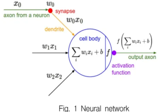
Fig. 1 Neural network
Figure 1 shows the model for artificial neural network (ANN) used in AI modeling. Input spikes in the brain can be expressed as
,
, and
and are multiplied by weighting numbers
,
, and
. Adjusting the weights is the core of neural networks. If the result from the weighting computation is larger than the threshold value in the cell body, the output signal can be activated and transferred to other parts of the neural network[1].Digital computing, which was conventionally used in AI processors, faced the problem of consuming large amounts of power[2]. To overcome the power dissipation problem, current-mode analog circuit design technique have been proposed as a candidate for a low power AI processor because current-mode analog circuit has the feature that can have a constant power consumption regardless of operating frequency [3-6].
Figure 2 shows the basic computational block diagram of current-mode AI processor. For ANN, weighting is one of the core circuits in current-mode signal processing. A current
multiplier circuit plays a significant role for the multiplication of the input signal with a weighted current value.
For realizing current-mode weighting circuit, translinear loop principles have been widely used for multiplier circuits[7-8]. Multiplication is realized with the concept of the square-law characteristics
Fig. 2 Basic computational block diagram of current-mode AI processor
in MOSFET. Linearity is important but also the range in which the multiplier can handle should be also considered [9-10]. This paper presents a four-quadrant analog multiplier circuit with the basis of a dual translinear loop model for satisfying the requirement of a higher linearity, reducing error mismatch and a wider dynamic range.
Ⅱ.
Dual Translinear LoopMultiplication is realized with the concept of the square-law characteristics in MOSFET. In a MOS transistor operating in the saturation region, current from drain to source,
, can be defined as
(1)
(2)
(3)where, K is the transconductance parameter,
is the threshold voltage,
is the gate-to-source voltage,
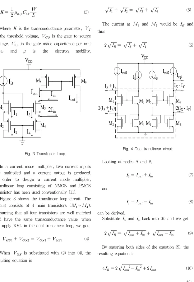
is the gate oxide capacitance per unit area, and µ is the electron mobility.Fig. 3 Translinear Loop
In a current mode multiplier, two current inputs are multiplied and a current output is produced.
In order to design a current mode multiplier, translinear loop consisting of NMOS and PMOS transistor has been used conventionally [11].
Figure 3 shows the translinear loop circuit. The circuit consists of 4 main transistors (
∼
).Assuming that all four transistors are well matched and have the same transconductance value, when we apply KVL in the dual translinear loop, we get
(4)When
is substituted with (2) into (4), the resulting equation is
(5)The current at
and
would be
and thus
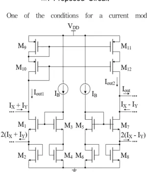
(6)Fig. 4 Dual translinear circuit
Looking at nodes A and B,
(7)and
(8)can be derived.
Substitute
and
back into (6) and we get
(9) By squaring both sides of the equation (9), the resulting equation is
(10)From this equation,
can be expressed as
(11)Figure 4 shows the dual translinear loop for deriving the current multiplication using two translinear loops. The principle behind the circuit is based on the square-difference identity as shown in (12).
(12)Basing the square-difference identity in the circuit in Fig. 4, we can reconstruct the equation in (11) to get
(13)and
(14)Since,
(15)
(16)
Finally, the multiplication concept was derived in (17)
(17)
Therefore, the current multiplier can be designed with this concept using dual translinear loops.
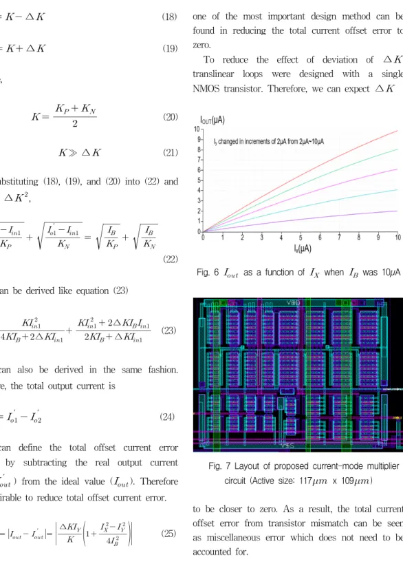
Ⅲ. Proposed Circuit
One of the conditions for a current mode
Fig. 5 Proposed current-mode multiplier circuit
multiplier is being able to multiply a current input with another current input. If
is a constant equal to 10µA, equation (17) would be a multiplication between
and
. However, by having different inputs, this circuit can function as either a multiplier or a divider.In a conventional multiplier circuit, the dual translinear loop consisted of PMOS and NMOS transistors. For an ideal case, transconductance
=
is assumed, because of a well matched transistor. However, in a more realistic approach, we must consider
≠
.∆
, error derived from mismatch, is not negligible in a real circuit.Therefore, we can assume that the offset value of physical parameter,
∆
has some value.
∆
(18)
∆
(19)where,
(20)
≫ ∆
(21)By substituting (18), (19), and (20) into (22) and ignoring
∆
,
′
′
(22)
′ can be derived like equation (23)′
∆
∆
∆
(23)
′ can also be derived in the same fashion.Therefore, the total output current is
′
′
′ (24)We can define the total offset current error (
) by subtracting the real output current value (
′ ) from the ideal value (
). Therefore it is desirable to reduce total offset current error.
′
∆
(25)Figure 5 shows the proposed current-mode multiplier circuit. From the derivation result of (25),
one of the most important design method can be found in reducing the total current offset error to zero.
To reduce the effect of deviation of
∆
, translinear loops were designed with a single NMOS transistor. Therefore, we can expect∆
Fig. 6
as a function of
when
was 10µAFig. 7 Layout of proposed current-mode multiplier circuit (Active size: 117
x 109
)to be closer to zero. As a result, the total current offset error from transistor mismatch can be seen as miscellaneous error which does not need to be accounted for.
Ⅳ. Experimental Simulation Result
Figure 6 shows the experimental simulation result of the current mode multiplier circuit
as a function of
. The circuit was simulated where
was kept at a constant of 10µA,
changed in increments of 2µA from 2µA ~ 10µA and
wasFig. 8 Wide dynamic range of
as a function of
when
was 10µAFig. 9 Total harmonic distortion
swept from
to
. Only positive current inputs were tested as current direction is positive in ANN system.The circuit was simulated using Magna Chip / SK Hynix 0.35
process technology. Thetransistor model was BSIM3v3 and the performance was analyzed through post-layout simulation using Cadence MMSIM.
Figure 7 shows the layout of the proposed current-mode multiplier circuit. The active area of the proposed circuit was 117
x 109
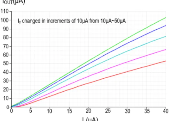
.Figure 8 shows the wide dynamic range of
as a function of
when
was 10µA,
changed in increments of 10µA from 10µA ~ 50µA, and
was swept from a range of 0 ∼ 40µA.Multiple transistors was added to the dual translinear loop so that the circuit can handle higher inputs for producing higher outputs. The output current was continually linear even past the 40µA range. From the calculation result using Cadence MMSIM, maximum total harmonic distortion (THD) that can be used to express linearity was observed as 0.3% when input current is 10 uA with 1 MHz operating frequency, as seen in Fig. 9.
Ⅴ. Conclusion
This paper presents a four-quadrant analog multiplier circuit with the basis of a dual translinear loop consisting of only NMOS transistors to get rid of transistor mismatch error which allowed for better linearity. The experimental simulation results show that by adding more transistors to the dual translinear loop circuit, good linearity can be seen even in higher current input ranges. Maximum THD was observed as 0.3%.
The proposed circuit is expected to be useful as the core circuit of current mode AI processor because of its wider range, reduced error, and higher linearity.
감사의 글
이 연구는 서울과학기술대학교 교내 일반과제 연구비 지원으로 수행되었습니다.
References
[1] W. Alaloul, “An Artificial Neural Networks (ANN) Model for Evaluating Construction Project Performance Based on Coordination Factors,” Cogent Engineering, vol. 5, no. 1, Aug. 2018.
[2] C. Enz and E. Vittoz, “CMOS Low-Power Analog Circuit Design,” Emerging Technologies: Designing Low Power Digital Systems, May 1996, pp. 79-133.
[3] H. Elwan and A. Soliman, “Low-Voltage Low-Power CMOS Current Conveyors,”
Circuits and Systems I: Fundamental Theory and Applications, IEEE Transactions on;, vol.
44, Sept. 1997, pp. 828-835.
[4] S. Yeo, J. Kim, T. Cho, S. Cho, and S. Kim,
“Design of Low Power Current Memory Circuit based on Voltage Scaling,” J. of the Korea Institute of Electronic Communication Science, vol. 11, no. 2, 2016, pp. 159-164.
[5] S. Park, H. Kim, D. Lee, and S. Kim, “A Low Power Current-Mode 12-bit ADC using 4-bit ADC in Cascade Structure,” J. of the Korea Institute of Electronic Communication Science, vol. 14, no. 6, Dec. 2019, pp. 1145-1152.
[6] S. Kim, “Performance Improvement of Current Memory for Low Power Wireless Communication MODEM,” J. of the Korea Institute of Electronic Communication Science, vol. 3, no. 2, 30 Apr. 2008, pp. 79-85.
[7] I. Aloui, N. Hassen, and K. Besbes, “A CMOS current mode four quadrant analog multiplier free from mobility reduction,” AEU - Int. J.
Electron Communications, vol. 82, 2017, pp.
119–126.
[8] A. Naderi and S. Ozoguz, “Design of high-linear, high-precision analog multiplier free from body effect,” Turkish J. Electrical Engineering and Computer Sciences, vol. 24, 2016 pp. 820-832.
[9] A. Amir and A. Ahmadi, “A Novel Current-Mode Four-Quadrant CMOS Analog Multiplier/Divider,” AEU – Int. J. of Electronics and Communications, vol. 66, no. 7, July 2012, pp. 581–586.
[10] K. Wawryn, “AB Class Current Mode Multipliers for Programmable Neural Networks,” Electronics Letters, vol. 32, no. 20, 1996, pp. 1902.
[11] A. Naderi, “A New High Speed and Low Power Four-Quadrant CMOS Analog Multiplier in Current Mode.” AEU – Int. J. of Electronics and Communications, vol. 63, no. 9, Sept. 2009, pp. 769-775.
저자 소개
이대니얼주헌(Daniel-Juhun Lee)
2014 ∼2018년 California State Univ ersity, Fullerton 졸업
2018년 ∼현재 서울과학기술대학교 대학원 IT융합공학과 석사과정 재학
※ 관심 분야 : AI용 아날로그 회로설계
김형민(Hyung-Min Kim)
2012 ∼2019년 서울과학기술대학교 전자IT미디어공학과 졸업2019년 ∼현재 서울과학기술대학교
대학원 정보통신미디어공학전공
석사과정 재학
※ 관심 분야 : AI용 아날로그 회로설계
박소연(So-Youn Park)
2016 ∼2020년 서울과학기술대학교 전자IT미디어공학과 졸업
2020년 ∼현재 서울과학기술대학교 대학원 미디어IT공학과 석사과정 재학
※ 관심 분야 : AI용 아날로그 회로설계
노태민(Tae-Min Nho)
2012 ∼2020년 서울과학기술대학교 전자IT미디어공학과 졸업
2020년 ∼현재 서울과학기술대학교 대학원 미디어IT공학과 석사과정 재학
※ 관심 분야 : AI용 아날로그 회로설계
김성권(Seong-Kweon Kim)
2002년 일본 TOHOKU대학 대학원 전자공학과(공학박사)
2002 ∼2004년 일본 TOHOKU대학 Assistant Professor & Research Fellow 2004~2009년 목포해양대학교 해양전자통신공학부 조교수
2009년~현재 서울과학기술대학교 전자IT미디어공학 과 교수
※ 관심분야 : 아날로그 회로 및 시스템